Optical Navigation Division
Device Processing in III-V Manufacturing:
Backside Wafer Processing
CS Mantech 2010 Workshop:
Overview of Device Processing in III-V Manufacturing
Timothy J Whetten and August Heffern, Avago Technologies
Eric F. Pabo, EV Group
Holly Rubin, Plasma-Therm LLC

Timothy J Whetten
Wireless Semiconductor Division
Why, why, why!Electrical:
A 94 GHz Monolithic Switch with a Vertical PIN Diode Structure, John Putnam, Mike Fukuda, Peter Staecker, Yong-
Hoon Yun, Gallium Arsenide Integrated Circuit (GaAs IC) Symposium, 1994. Technical Digest 1994., pp 333ff
Thermal:
A Backside Via Process For Thermal Resistance Improvement Demonstrated Using GaAs HBTs, J.S. Kofol, B.J.F. Lin,
M. Mierzwinski, A. Kim, A. Armstrong, R. Van Tuyl, Gallium Arsenide Integrated Circuit (GaAs IC) Symposium, 1992. Technical Digest
1992.
Process Considerations for Manufacturing 50 µm Thinned III-V Wafers, G. Cobb, H. Isom, C. Sellers , V. Williams, CS
MANTECH Conference, May 14-17, 2007, Austin, Texas, USA
Functional:
High Yield Intra-Cavity Interconnection Fabrication Method And Characterization Methodologies, M. Yajima, P.
Chang-Chien, X. Zeng, K. Luo, C. Cheung, K. Tornquist, and M. Barsky, CS MANTECH Conference, May 14-17, 2007,
Austin, Texas, USA 151ff
Packaging:
High Yield Intra-Cavity Interconnection Fabrication Method And Characterization Methodologies, M. Yajima, P.
Chang-Chien, X. Zeng, K. Luo, C. Cheung, K. Tornquist, and M. Barsky, CS MANTECH Conference, May 14-17, 2007,
Austin, Texas, USA 151ff
Density:
Product performance:
Page 2

Timothy J Whetten
Wireless Semiconductor Division
Thermal
Electrical
PackagingFunctional
Page 3

Timothy J Whetten
Wireless Semiconductor Division
Process Flow - High Level
Mount
Thin
Via
Metal
Demount
Dice
Bond (permanent or temporary)
Grind
Photo/Etch
Dep/Photo/Etch (or liftoff)
Debond
Page 4

Timothy J Whetten
Wireless Semiconductor Division
Process Flow - High Level
Mount
Thin
Via
Metal
Demount
Dice
Grind
Photo/Etch
Dep/Photo/Etch (or liftoff)
Debond
Page 5

Timothy J Whetten
Wireless Semiconductor Division
Aligned wafer bonding - overview
Slide courtesy
of EV Group
Page 6

Timothy J Whetten
Wireless Semiconductor Division
Types of Bonding
Wafer Bonding
(1)
Intermediate
Layer
No
Intermediate
Layer
Metal
Glass
Polymer (2, 3)
Fusion (5)
Anodic
Thermocompression (6)
Solder
Eutectic
Thermoset
UV Set (7)
Thermoplastic
Glass FritNOTES
1. May be mechanically or optically aligned. Bonding process will
effect final alignment results
2. May be used for permanent or temporary bonding.
3. Inludes adhesive bonding
4. TLP – Transient Liquid Phase
5. Also called direct bonding or molecular bonding. Has strict
requirements for flatness, surface finish, and contamination.
6. Also called metal diffusion
7. Requires special bond chamber.
TLP (4)
Slide courtesy
of EV Group
Page 7

Timothy J Whetten
Wireless Semiconductor Division
Bonding Process Requirements
No Intermediate Layer Intermediate Layer
Anodi c
Bondi ng
( Electric Fiel d)
Direct
Bonding
Pl asma
Act ivat ed
Di rect
Bonding
Glass Fr it
Ther m
o
Compr ession
Solder /
Eut ectic / TLP
Adhesive
Epoxy
( ther m
al ly
cured)
Epoxy
(UV cured)
Surface
Roughness< 20 nm < 0.5nm < 2 nm < 1000 nm < 2 nm < 1000 nm < 1000 nm < 1000 nm < 1000 nm
Layer Thickness NA NA NA
Determined
by silk
screen
process
~ 1000 nm
each side
~ 1000 nm
each side? ? ?
Process
Temperature400 - 500 C
1000 C
(anneal)
Room Temp
& 200-300 C
anneal
400 - 500 C
300 - 500 C
depending
on metal
200 -500 C
depenting
on metal
< 200 C
depending
on adhesive
< 200 C
depending
on adhesive
~ Room
Temperature
Cleanroom
Environment
(FS209E)
100 10 or 1 10 1000 10 100 100 1000 1000
Sensitivity to
ParticlesMedium High High Low Medum Medium Low Low Low
Sensitivity to
Surface
Contamination
Medium Very High Very High Medium High High Low Low Low
Na present Yes No No No No No No No No
Cycle Time
(minutes)45 - 90
Bond ~ 1
Anneal - hrs
Bond ~ 1
Anneal hrs45 - 90 30 - 90 30 - 60 5 - 45 15-30 5 -15
Slide courtesy
of EV Group
Page 8
Timothy J Whetten
Wireless Semiconductor Division
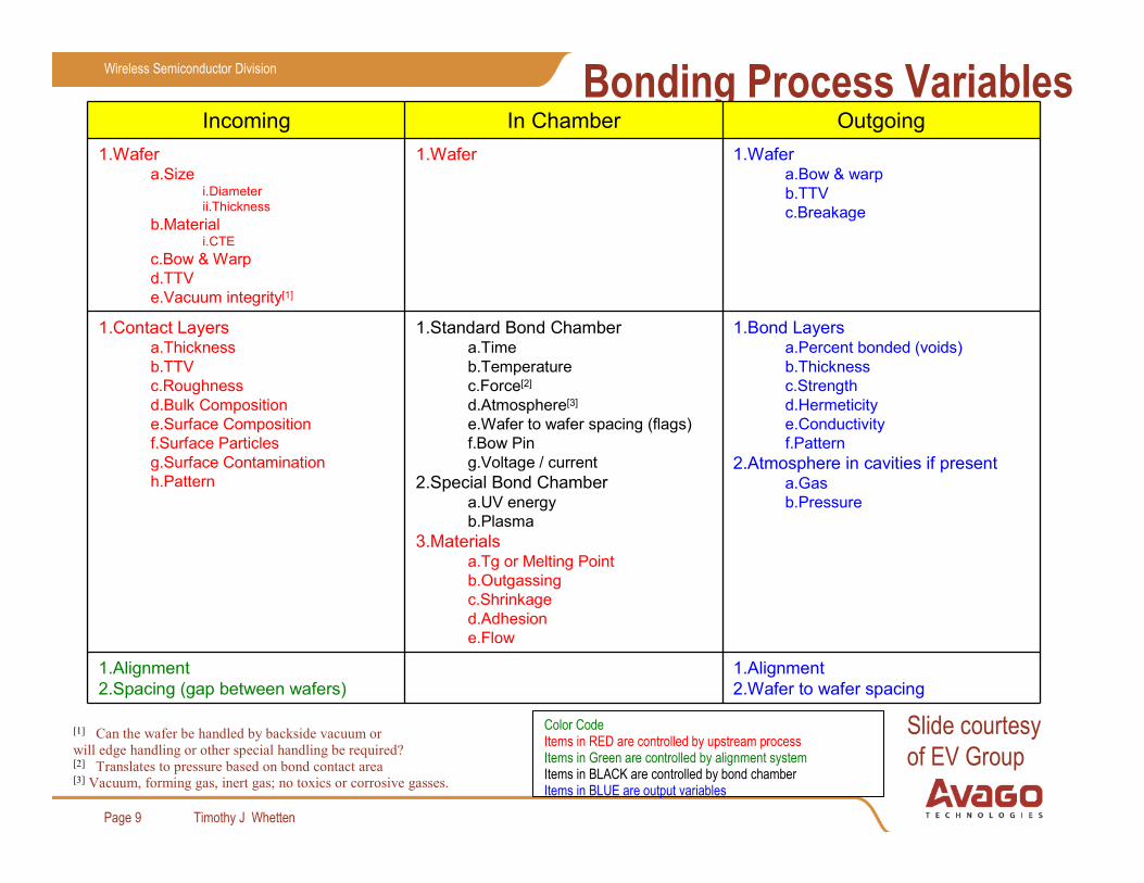
Bonding Process Variables
Color CodeItems in RED are controlled by upstream processItems in Green are controlled by alignment systemItems in BLACK are controlled by bond chamberItems in BLUE are output variables
Incoming In Chamber Outgoing
1.Wafera.Size
i.Diameter
ii.Thickness
b.Materiali.CTE
c.Bow & Warp
d.TTV
e.Vacuum integrity[1]
1.Wafer 1.Wafera.Bow & warp
b.TTV
c.Breakage
1.Contact Layersa.Thickness
b.TTV
c.Roughness
d.Bulk Composition
e.Surface Composition
f.Surface Particles
g.Surface Contamination
h.Pattern
1.Standard Bond Chambera.Time
b.Temperature
c.Force[2]
d.Atmosphere[3]
e.Wafer to wafer spacing (flags)
f.Bow Pin
g.Voltage / current
2.Special Bond Chambera.UV energy
b.Plasma
3.Materialsa.Tg or Melting Point
b.Outgassing
c.Shrinkage
d.Adhesion
e.Flow
1.Bond Layersa.Percent bonded (voids)
b.Thickness
c.Strength
d.Hermeticity
e.Conductivity
f.Pattern
2.Atmosphere in cavities if presenta.Gas
b.Pressure
1.Alignment
2.Spacing (gap between wafers)
1.Alignment
2.Wafer to wafer spacing
[1] Can the wafer be handled by backside vacuum or
will edge handling or other special handling be required?[2] Translates to pressure based on bond contact area[3] Vacuum, forming gas, inert gas; no toxics or corrosive gasses.
Slide courtesy
of EV Group
Page 9

Timothy J Whetten
Wireless Semiconductor Division
Types of Alignment for Bonding Slide courtesy
of EV Group
Page 10

Timothy J Whetten
Wireless Semiconductor Division
Optical bond alignment for the EVG®500 series
Optical bond alignment and wafer bonding are separated
Bond aligner: Wafers are aligned and fixed to a bond chuck
Wafer bonder: Wafers are bonded (pressure, temperature, vacuum)
Bond chuck transfer
EVG540EVG510
EVG520ISSmartView
EVG620
EVG6200
IQ Aligner
EVG560
Slide courtesy
of EV Group
Page 11

Timothy J Whetten
Wireless Semiconductor Division
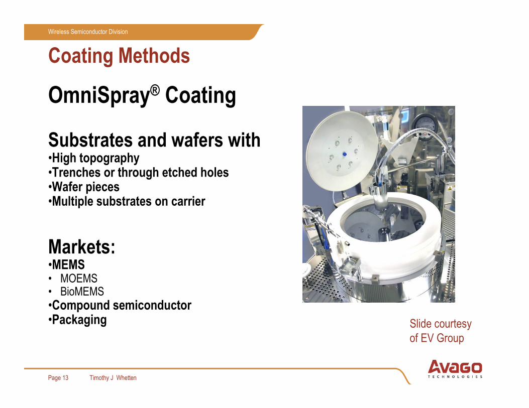
Coating Methods
Spin CoatingWafers•Blank wafers•Wafers with little to no Topography•Square substrates (without topography)•Bump wafers
Markets – All: •Standard semiconductor•MEMS•Power devices•Optical systems•Packaging
Slide courtesy
of EV Group
Page 12
Timothy J Whetten
Wireless Semiconductor Division
Coating Methods
OmniSpray® Coating
Substrates and wafers with •High topography•Trenches or through etched holes•Wafer pieces•Multiple substrates on carrier
Markets:•MEMS• MOEMS• BioMEMS
•Compound semiconductor•Packaging Slide courtesy
of EV Group
Page 13

Timothy J Whetten
Wireless Semiconductor Division
OmniSpray® Coating Application
1. 10µm layer with BCB 4026-46 Spin coating (area dispense)2. 5µm layer with BCB 4024-40 Spin coating (area dispense)
3. 10 µm layer with BCB 4026-46 Spray coating4. 5µm layer with BCB 4024-40 Spray coating
33003000
1200942
1,5
3
7
8
0
500
1000
1500
2000
2500
3000
3500
4000
1 2 3 4
BC
B-C
on
sum
pti
on
[µ
l]
0
1
2
3
4
5
6
7
8
9
10
Un
ifo
rmit
y [
%]
Spin
Spray
BCB Coating tests on 8" Si-Wafer
Slide courtesy
of EV Group
Page 14

Timothy J Whetten
Wireless Semiconductor Division
Process Flow - High Level
Mount
Thin
Via
Metal
Demount
Dice
Bond (permanent or temporary)
Photo/Etch
Dep/Photo/Etch (or liftoff)
Debond
Page 15

Timothy J Whetten
Wireless Semiconductor Division
CS-Specific ConsiderationsCS are very brittle after backgrind
• Standard backgrind tape provides insufficient support for subsequent wafer handling/processing when thinning below 200um
� Support carriers generally required
� Bonding process becomes critical to ensure 100% enclosure & support of device wafer by carrier wafer (minimize grind damage)
Backgrind wheel selection
• To prevent unwanted damage of GaAs, proper wheel selection critical to provide efficient cutting with minimal force
Post-grind etching / polishing
• Required to provide stress relief of ground wafer & etch through grind-induced damage
� Chemical selection important to provide isotropic etch
� CMP an alternative to wet chemical etch
• Etch / polish also improves surface quality of ground material
Page 16

Timothy J Whetten
Wireless Semiconductor Division
Backgrind Process
Typical method of grinding is top-down in-feed of grind wheel to rotating vacuum grind chuck
• Others methods such as creep-feed (wafer fed laterally through grind wheel) exist as well
Wafer held in place by vacuum chuck. Removal occurs via feed of grind wheel assembly through wafer with concurrently rotating grind wheel and chuck
Two grinds / wheels:
• Coarse grind: bulk removal of material at high feed rates using harder wheel
• Fine grind: final material removal at slow feed rates using softer wheel
�Removes damage incurred during coarse grind & provides more polished surface of wafer
�Grind removal amount balanced with feed rates to reduce throughput considerations
Page 17

Timothy J Whetten
Wireless Semiconductor Division
Support Carrier
Device Wafer
Bonding Layer
Vacuum Chuck
Grind Wheel
Pre-Grind Post-Grind
Thickness
“Thickness” or removal controlled by in-situ probe(s) during grind. Allows for support/bond/device stack thickness to be targeted to a specific value (prior
knowledge of support & bond layers is required), or a pre-determined thickness of material to be removed from the device wafer.
Support Carrier
Device WaferBonding Layer
Vacuum Chuck
Grind Wheel
Thickness
Backgrind Process
Page 18

Timothy J Whetten
Wireless Semiconductor Division
Backgrind process control parameters
• Primary
�Grind wheel rotational speed
�Vacuum chuck rotational speed
�Grind wheel feed rates
• Secondary
�Cutting H2O flow rates & application
�Chuck cleanliness (planar chuck surface required to reduce grind defects)
�Chuck vacuum capability (entire wafer required to be held firmly in place during grind to reduce wafer fluttering & damage)
�Grind wheel angles & direction (can be adjusted to achieve optimal TTV & minimize wafer damage)
Page 19

Timothy J Whetten
Wireless Semiconductor Division
Resinoid wheels best suited for GaAs backgrind
• Key grind wheel considerations:
�Diamond mesh size
�Diamond concentration
�Bond material hardness
�Bond material porosity & distribution
Selected based on above criteria balances self-dressing needs, wheel lifespan, and device wafer surface finish
Example grind wheel tooth magnified image
Grind wheel selection Critical to uniform thickness targeting & surface finish
Page 20

Timothy J Whetten
Wireless Semiconductor Division
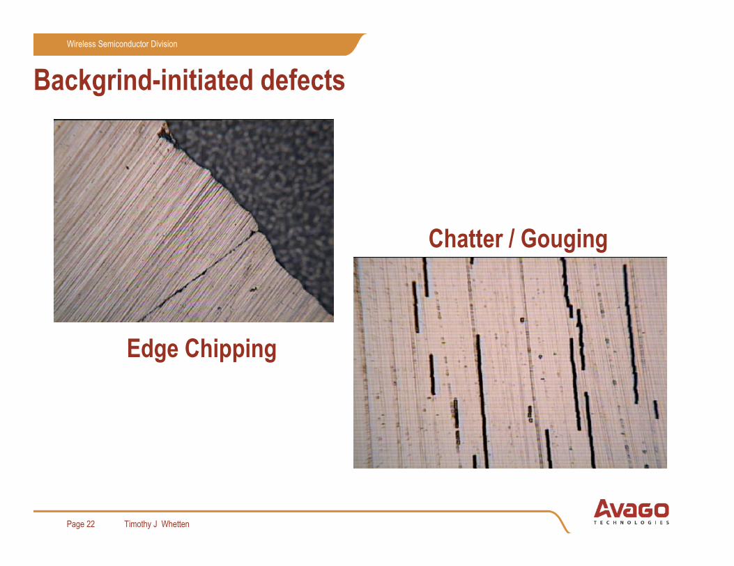
• Star cracks – caused by debris on the chuck or embedded debris in the bondinglayer
• Edge chipping – caused by poor edge bonding resulting in unbonded material becoming over-ground and breaking off
• Over-grind – usually initiated by non-uniform bonding layer thickness or poor bond allowing for water encroachment between the device & support wafers. Over-grind results in a region much thinner than surrounding areas and appears to have a burnished appearance
• Chatter & Gouging – caused by grind debris or low-hanging diamonds in the wheel that create deep gouges in the wafer surface
• Cross-hatching – caused by non-uniform grind tooth wear, leading to grind marks that run counter to the majority
Backgrind-initiated defects
Page 21
Timothy J Whetten
Wireless Semiconductor Division
Backgrind-initiated defects
Edge Chipping
Chatter / Gouging
Page 22

Timothy J Whetten
Wireless Semiconductor Division
Post-grind Cleaning
Post-grind cleaning is required to remove residual grind debris from wafer surfaces and prevent contamination of downstream tools
Many grind tools utilize some form of in-situ cleaning prior to wafer exit
• Spin/rinse stations
• Backside brush scrubbing
Occasionally, in-situ cleaning is insufficient, and additional cleaning methods are required
• Brush scrubbing tools provide effective cleaning of grind debris
Page 23

Timothy J Whetten
Wireless Semiconductor Division
Post-Grind Etch/Polish
Post-backgrind wet chemical etch and/or polishing is required on GaAsmaterial to relieve grind-induced stress and reduce roughness of surfaces
•Wet chemical relief etch chemistries need to be tailored to remove desired amount of material in uniform fashion. Typical chemicals can include:
�Hydrogen peroxide
�Ammonium hydroxide
�Phosphoric acid
•Isotropic etching is desired so as to minimize decoration of grind defects. Tool selection can be critical to allow for well-controlled etching
•CMP can be used as an alternative to wet chemical post-grind processing
Page 24

Timothy J Whetten
Wireless Semiconductor Division
Post-Grind Etch/PolishPost-grind etching can expose & highlight subsurface grind damage depending on chemistry
• Damage can become visible to naked eye
Page 25

Timothy J Whetten
Wireless Semiconductor Division
Process Flow - High Level
Mount
Thin
Via
Metal
Demount
Dice
Bond (permanent or temporary)
Grind
Dep/Photo/Etch (or liftoff)
Debond
Page 26

Timothy J Whetten
Wireless Semiconductor Division
Background device wafer
Cap wafer
Alignment keys
Photoresist
Mask
Topside objectives
Bottom IR illumination
IR alignment
Page 27

Timothy J Whetten
Wireless Semiconductor Division
Background device wafer
Clear carrier wafer
Alignment keys
Photoresist
Bottom objectives
Backside alignment
Page 28

Timothy J Whetten
Wireless Semiconductor Division
Mask Aligned mask and wafer
Example of IR alignment features
Page 29

Timothy J Whetten
Wireless Semiconductor Division
Example of backside alignment features
Mask
Digitized image of mask
Wafer Aligned mask and wafer
Page 30

Timothy J Whetten
Wireless Semiconductor Division
Process Flow - High Level
Mount
Thin
Via
Metal
Demount
Dice
Bond (permanent or temporary)
Grind
Dep/Photo/Etch (or liftoff)
Debond
Page 31

Timothy J Whetten
Wireless Semiconductor Division
Process Requirements
Good Electrical Performance
• Etched Via Easily Metalized
• Feature Profile Control
• Good CD Control
• Smooth Feature Sidewalls
• No Post-Etch Residues
• Selective to Underlying Metal
Short Process time
• Fast / Uniform GaAs Etch Process
• Resist Etch Mask
Robust Process
• Tolerant of Upstream Variations
Slide courtesy of
Plasma-Therm LLC
Page 32

Timothy J Whetten
Wireless Semiconductor Division
Via Profile Control
Vertical Etch Profile
Sloped Etch Profile
Sloped PR
Slide courtesy of
Plasma-Therm LLC
Page 33

Timothy J Whetten
Wireless Semiconductor Division
Via Profile Control
Vertical
Benefits:
• Good CD Control
• Process Reproducibility
Issues:
• More Difficult to Metalize
• Sidewall Passivation Removal
Slide courtesy of
Plasma-Therm LLC
Page 34

Timothy J Whetten
Wireless Semiconductor Division
Via Profile Control
Sloped
Eroding a Sloped Resist Etches a Sloped Via Profile
GaAs
Resist
Slide courtesy of
Plasma-Therm LLC
Page 35

Timothy J Whetten
Wireless Semiconductor Division
Via Profile Control
Sloped
Benefits:
• Good CD Control at Front Side
• Process Reproducibility
Issues:
• Profile Highly Dependent on Initial PR Profile
• Roughened Sidewalls
• Sidewall Passivation Removal
• Discontinuous Slope
Slide courtesy of
Plasma-Therm LLC
Page 36

Timothy J Whetten
Wireless Semiconductor Division
Via Profile Control
Sloped – Resist ErosionSeveral Key Factors Combine for Effective Profile Control
• Initial Photoresist Profile
• Process Conditions
• Selectivity (GaAs : PR)
• Chemistry
• RF Power Levels (Bias)
• Temperature
Slide courtesy of
Plasma-Therm LLC
Page 37
Timothy J Whetten
Wireless Semiconductor Division
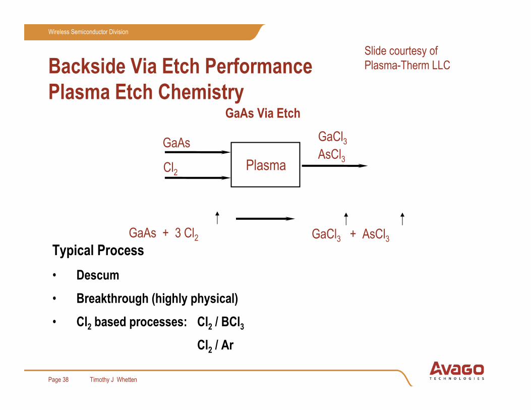
Backside Via Etch Performance
Plasma Etch Chemistry
Typical Process
• Descum
• Breakthrough (highly physical)
• Cl2 based processes: Cl2 / BCl3
Cl2 / Ar
GaAs Via Etch
Plasma
GaAs + 3 Cl2 GaCl3 + AsCl3
GaAs
Cl2
GaCl3AsCl3
Slide courtesy of
Plasma-Therm LLC
Page 38

Timothy J Whetten
Wireless Semiconductor Division
Backside Via Etch Performance
Plasma Etch Chemistry
Conventional GaAs via etching involves the use of a chlorine (Cl2) based process chemistry
Additive gases like BCl3, Ar, or CH4 are incorporated for profile or selectivity control
• Cl2/BCl3 chemistry in a 4:1 or 5:1 gas ratio is a proven production worthy process on the Plasma-Therm Versaline yielding high etch rates and selectivities.
Chemistry Cl2 only Cl2 and BCl3
Etch Rate 5 µm/min 9 µm/min
Slide courtesy of
Plasma-Therm LLC
Page 39

Timothy J Whetten
Wireless Semiconductor Division
Backside Via Etch Performance
Aspect Ratio Dependent Etching
0
2
4
6
8
10
12
14
0.0 0.5 1.0 1.5 2.0 2.5 3.0
Aspect Ratio (etch depth/feature size)
Average Etch Rate (microns/min)
Slide courtesy of
Plasma-Therm LLC
Page 40
Timothy J Whetten
Wireless Semiconductor Division
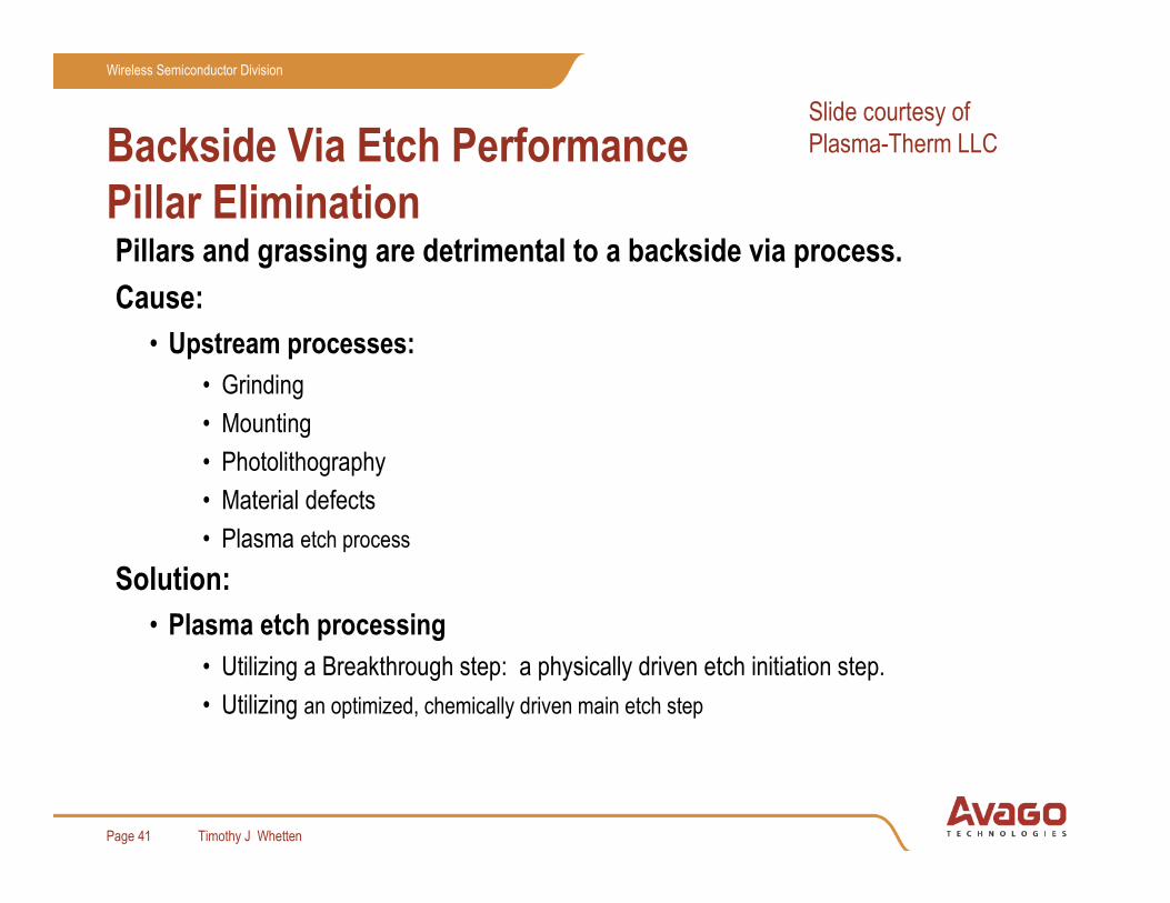
Backside Via Etch Performance
Pillar EliminationPillars and grassing are detrimental to a backside via process.
Cause:
• Upstream processes:
• Grinding
• Mounting
• Photolithography
• Material defects
• Plasma etch process
Solution:
• Plasma etch processing
• Utilizing a Breakthrough step: a physically driven etch initiation step.
• Utilizing an optimized, chemically driven main etch step
Slide courtesy of
Plasma-Therm LLC
Page 41

Timothy J Whetten
Wireless Semiconductor Division
Manufacturability
ICP Based Via Etch ProcessInductively Coupled Plasma (ICP) GaAs Via Etch Process
Independent Control RF Bias / Density
• GaAs Etch Rate vs. GaAs : Resist Selectivity
• Via Profile Control
High Density Plasma
• High Etch Rate for High Throughput
High Conductance Design
• Low Pressure Operation
• Excellent Within Wafer Uniformity
Slide courtesy of
Plasma-Therm LLC
Page 42

Timothy J Whetten
Wireless Semiconductor Division
Manufacturability
Controlled ICP Source Heating
Controlled ICP Source Heating
• Process Stability
• Reduced Maintenance
• Constant Chamber Conditions
Heated ceramic spool and lidICP Cross-section
Slide courtesy of
Plasma-Therm LLC
Page 43

Timothy J Whetten
Wireless Semiconductor Division
Seed dep and plate
Plating is remarkably insensitive to via profile
(however this profile isn’t considered “ideal”)
This image is the author’s alone and does not
represent typical processing by any of his friends
and colleagues (except the great job plating).
Page 44

Timothy J Whetten
Wireless Semiconductor Division
Process Flow - High Level
Mount
Thin
Via
Metal
Demount
Dice
Bond (permanent or temporary)
Grind
Photo/Etch
Dep/Photo/Etch
Page 45

Timothy J Whetten
Wireless Semiconductor Division
DeBonding – Process Overview
Single Wafer Carrier
ThinWafer Cassette
FilmFrame Cassette
Coin Stack Wafer-Canister
DeBondingDeBonding HandlingHandling Output FormatOutput Format
etc.…
Megasonic
DI-Water
Solvent
Diluted Chemistry
HighPressure
BrushScrubber
CleaningCleaning HandlingHandling
etc………..
wedge-off
slide-off
UV-debond
Slide courtesy
of EV Group
Page 46

Timothy J Whetten
Wireless Semiconductor Division
DeBonding – Process FlowEVG850DB EVG850DB
Brewer Adhesive, FilmFrame Output
Slide courtesy
of EV Group
Page 47
Timothy J Whetten
Wireless Semiconductor Division
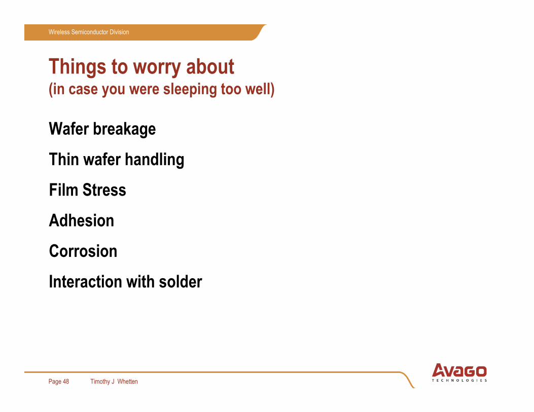
Things to worry about (in case you were sleeping too well)
Wafer breakage
Thin wafer handling
Film Stress
Adhesion
Corrosion
Interaction with solder
Page 48

Timothy J Whetten
Wireless Semiconductor Division
Edge-trimming process prior bonding
� Enables of using SEMI-standard carrier wafer
� Rectangular wafer edge, resulting in higher die strength
(as reported per Philips, Netherlands)
� Wafer is slightly smaller after thinning, enabling full support
(no resulting sharp wafer-edge)
� Minimized contamination of grinding-wheel
Eliminating Edge ChippingSlide courtesy
of EV Group
Page 49

Timothy J Whetten
Wireless Semiconductor Division
Courtesy of Dongshun Bai - Brewer Science;
to be presented at ISTC/CSTIC 2009; “Edge Protection of Temporarily Bonded Wafers during Backgrinding”
50µm
Investigation on different potential
approaches has been realized;
After temporary bonding + thinning step,
edge defects have been statistically
characterized.
Edge-trimming of device wafer prior
bonding is showing significant less
defects compared to other approaches.
Eliminating Edge ChippingSlide courtesy
of EV Group
Page 50

Timothy J Whetten
Wireless Semiconductor Division
Backside Processing plus Wafer Scale Packaging
Photograph of the first GaAs Wafer Scale Package products on the market in the 0402 form factor (1mm x
0.5mm x 0.3mm) next to a standard 0402 inductor
Page 51

Timothy J Whetten
Wireless Semiconductor Division
Henrik Morkner, “GaAs-Based Surface Mount Wafer Scale Package MMICs for DC to 45 GHz Applications”http://avagotechwireless.com/collateral/AV02-2103EN.pdf
K. Phan, J. Kessler, H. Morkner, M. Vice, L. Nguyen, J. Roland, “A Miniaturized Wafer-Scale Package Demonstrated with Three Enhancement Mode Amplifiers”, EuMC 2008, October 2008
Backside Processing plus Wafer Scale Packaging
Page 52

Timothy J Whetten
Wireless Semiconductor Division
Simplified assembly process
Page 53
Timothy J Whetten
Wireless Semiconductor Division
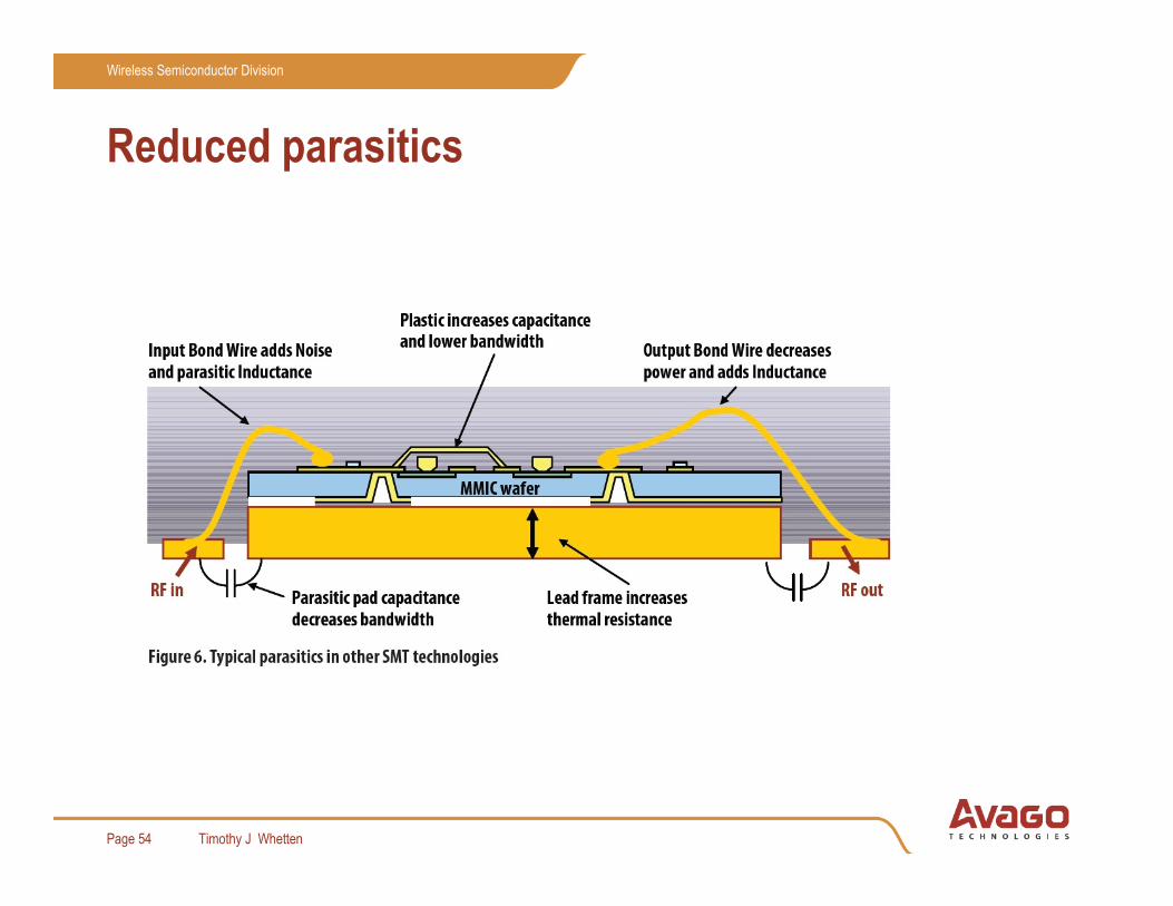
Reduced parasitics
Page 54

Timothy J Whetten
Wireless Semiconductor Division
Process Flow - Examples
Temporary Mount
Thin
Dice
Temporary Mount
Thin
Via
Metal
Demount
Dice
Permanent Mount
Thin
Via
Metal
Dice
Thin
Demount
Page 55


