
DESIGN OF HIGHLY EFFICIENT GRID CONNECTED
MICROINVERTER FOR PHOTOVOLTAIC PANEL
V MANI VIKASH (111EE0612)
SANDEEP KUMAR (111EE0430)
Department of Electrical Engineering
National Institute of Technology Rourkela
DESIGN OF HIGHLY EFFICIENT GRID CONNECTED
MICROINVERTER FOR PHOTOVOLTAIC PANEL

DESIGN OF HIGHLY EFFICIENT GRID CONNECTED
MICROINVERTER FOR PHOTOVOLTAIC PANEL
A Thesis submitted in partial fulfillment of the requirements for the degree of
Bachelor of Technology in “Electrical Engineering”
By
V MANI VIKASH (111EE0612)
SANDEEP KUMAR(111EE0430)
Under guidance of
Prof. SOMNATH MAITY
Department of Electrical Engineering
National Institute of Technology
Rourkela-769008 (ODISHA)
May-2015

i
DEPARTMENT OF ELECTRICAL ENGINEERING
NATIONAL INSTITUTE OF TECHNOLOGY,
ROURKELA
ODISHA, INDIA-769008
CERTIFICATE
This is to certify that the thesis entitled “ Design of Highly Efficient Grid connected
Microinverter for Photovoltaic Panel”, submitted by V Mani Vikash (Roll. No.
111EE0612) in partial fulfilment of the requirements for the award of Bachelor of
Technology in Electrical Engineering during session 2014-2015 at National Institute of
Technology, Rourkela. A bonafide record of research work carried out by them under my
supervision and guidance.
The candidates have fulfilled all the prescribed requirements.
The Thesis which is based on candidates’ own work, have not submitted elsewhere for a
degree/diploma.
In my opinion, the thesis is of standard required for the award of a bachelor of technology
degree in Electrical Engineering.
Place: Rourkela
Dept. of Electrical Engineering Prof.Somnath Maity
National institute of Technology Assistant Professor
Rourkela-769008

ii
DEPARTMENT OF ELECTRICAL ENGINEERING
NATIONAL INSTITUTE OF TECHNOLOGY,
ROURKELA
ODISHA, INDIA-769008
CERTIFICATE
This is to certify that the thesis entitled “Design of Highly Efficient Grid connected
Microinverter for Photovoltaic Panel”, submitted by Sandeep Kumar (Roll. No.
111EE0430) in partial fulfilment of the requirements for the award of Bachelor of Technology
in Electrical Engineering during session 2014-2015 at National Institute of Technology,
Rourkela. A bonafide record of research work carried out by them under my supervision and
guidance.
The candidates have fulfilled all the prescribed requirements.
The Thesis which is based on candidates’ own work, have not submitted elsewhere for a
degree/diploma.
In my opinion, the thesis is of standard required for the award of a bachelor of technology
degree in Electrical Engineering.
Place: Rourkela
Dept. of Electrical Engineering Prof.Somnath Maity
National institute of Technology Assistant Professor
Rourkela-769008

iii
ACKNOWLEDGEMENTS
On the submission of my thesis report of “Design of Highly Efficient Grid Connected
Microinverter for photovoltaic panel”, I would like to extend my gratitude and sincere thanks
to my supervisor Prof. Somnath Maity, Asst. Professor of the Department of Electrical
Engineering, NIT Rourkela for his essential advice, support and constant motivation at every
step of this project in the past year. I am indebted to him for his esteemed guidance starting
from formation of the problem statement to final derivation and insights for the solution.
I also extend my gratitude to the researchers and engineers whose hours of toil has produced
the papers and theses that I have utilized in my project.
V Mani Vikash
Sandeep Kumar
B.Tech (Electrical Engineering)

iv
ABSTRACT
The Photo Voltaic (PV) energy system, utilized as a part of this undertaking, is another
idea being used, which is increasing huge ubiquity because of expanding significance to
developing option wellsprings of source of energy over exhaustion of customary non-
renewable energizes all around the globe. The systems which are being created concentrate on
making sun as source of energy in the most productive way and supply them to the accessible
loads without influencing their execution.
We are going to study the operational principle and the structure of the present grid-
connected photovoltaic system. Grid connected PV generation system is mainly composed of
the PV array, flyback converter and the micro inverter device. We will use flyback converter
to step up the 18 to 40V DC voltage to 400V DC and to also isolate from primary side to the
secondary side for protection purpose. We will use an improved PWM micro inverter control
system that can be applied in grid-connected PV generation to convert 400Vdc to 240V AC.
We will use PROTEUS and MATLAB/Simulink softwares to simulate and analyse. The result
of the simulation shows that output of PV which is 18 to 40V DC is stepped up 400V DC and
further to 240V AC using flyback converter and grid connected inverter respectively.

1
CONTENTS
Abstract iv
Contents 1
List of Figures 3
List of Tables 4
CHAPTER 1
INTRODUCTION
1.1 Motivation 6
1.2 Organization of Thesis 7
CHAPTER 2
PV ARRAY CHARACTERISTICS
2.1 Introduction 9
2.2 Photovoltaic Cell 9
2.3 Photovoltaic Modules 10
2.4 Photovoltaic Array 11
2.5 PV Array Modelling 11
2.6 I-V Characteristics of Solar cell 13
CHAPTER-3
SYSTEM DESCRIPTION
3.1 Flyback Converter 29
3.2 Flyback Converter without snubber 30
3.3 Design of Primary RC Snubber for Flyback converter
3.4 Inverter 36

2
3.5 sinusoidal pulse width modulation 37
3.6 Filter 40
3.7 Single Phase Grid tied inverter 42
3.8 Grid Synchronisation 42
CHAPTER-4
SIMULATION RESULTS
4.1 Overall System Description 42
4.2 Flyback Converter Simulation 42
4.3 Inverter Simulation 47
4.4 Conclusion 49
CHAPTER-5
CONCLUSION
5 Conclusion 51
References

3
LIST OF FIGURES
Fig. No Name of the Figure Page. No.
1 Schematic diagram of a simple photovoltaic system 9
2 Basic representation of photovoltaic effect 10
3 Equivalent circuit diagram of PV cell 11
4 Overall model of a PVcell 12
5 I-V Characteristics at cell temperature of 25°C 13
6 Flyback converter circuit 15
7 Flyback converter circuit without snubber 16
8 High frequency waveforms due to ringing 16
9 Flyback converter circuit with primary RC snubber 16
10 Overall Flyback converter circuit 18
11 Full bridge inverter 19
12 On and off conditions of thyristors in inverter 20
13 Sinusoidal pulse width modulation 21
14 Inverter circuit wit LC filter 22
15 Single phase grid tied inverter 22
16 Overall model of system 25
17 PWM of 40KHz for flyback converter 27
18 Simulation model of flyback converter in PROTEUS 27
19 Output voltage of flyback converter 28
20 PWM of 15KHz for inverter 29
21 Simulation model of inverter in PROTEUS 30
22 Output current waveform of inverter 30
23 Output voltage of inverter 31

4
LIST OF TABLES
Table. No. Name of the Table Page. No.
1.1 Comparison of 30 inverters (23 with transformer, 7 transformerless)
for single-phase grid-connected PV system ) 6
1.2 Ratings of flyback converter 18
1.3 Ratings of inverter 23

5
CHAPTER1
Introduction

6
1.1 MOTIVATION:
Previously, different distinctive topologies of inverter are proposed or are right now
utilized for low power, single-phase grid-connected photovoltaic (PV) Systems. A typical
innovation being used is a full-bridge inverter in mix with a Line-frequency transformer. The
transformer, be that as it may, is not a crucial prerequisite and Inverters without transformers
offer a few points of interest. A late European Market study demonstrates that Inverters
without transformers are profitable as for productivity, expense, weight, encapsulated vitality,
and size. Table 1.1 demonstrates the consequences of an examination of grid-connected
single-phase inverters for PV frameworks in the 1±2 kW power scope. Thirty inverters were
looked at, of which seven were without transformers and twenty three with transformer. The
gures for weight and cost are standardized to the inverters appraised power and particularly
the value contrast between the two inverter sorts is amazing (the transformerless type are
almost twenty five percent less expensive).
Other than beneficial transformerless ideas, multilevel inverters likewise guarantee
great arrangements, as these inverters are able to create "stepped" output voltage waveforms.
These waveforms are almost sinusoidal better than those created by traditional full-bridge
inverters. On AC side multilevel inverters need less filter effort, so the cost of inverter is less
expensive, less in weight and more conservative. Diverse levels of DC voltage levels are
essential, to produce multilevel output voltage waveforms. These can be given by partitioning
a PV array into proper sub-arrays
INVERTER TYPE MAX. EFFICIENCY
%
WEIGHT Kg/kW PRICE AS$/W
With transformer 93.1 16.1 1.95
Transformerless 95.9 12.3 1.47
Table 1.1 : Estimation of similarities of thirty inverters (twenty three with transformer and
seven without transformer) for grid-connected singlephase PV systems .
In this project we have chosen a flyback converter topology configuration on the
front-end converter, because we need to not only boost voltage level but also isolate from
primary side to the secondary side for protection purpose. The grid tied inverter as a back-
end converter will connect to the grid and transfer power as well.

7
1.2 ORGANISATION OF THESIS:
The thesis is organised into four chapters including the chapter of introduction. Each
chapter is different from the other and is described along with the necessary theory required
to comprehend it.
Chapter2 deals with PV Array Characteristics and its modelling. First, the solar cell
is described and various material technologies available for construction of solar cells are
seen. The equivalent mathematical modelling of the solar cell is made after studying various
representations and simplification is made for our purpose.
Chapter3 describes the flyback converter without snubber and with snubber
description and their various functions. It describes inverter description and its various
functions. The theory about Filters is discussed. Grid synchronisation is also studied here.
Why the active power and reactive need to be controlled is also discussed.
Chapter4 shows the practical implementation of the flyback converter, inverter and all
the simulation results obtained.
Chapter5 gives the conclusion of the project.

8
CHAPTER2
PV Array Characteristics

9
2.1 INTRODUCTION:
Photovoltaic permit the shoppers to produce electricity in a clean, solid and calm way.
Photovoltaic are frequently contracted as PV. Photovoltaic cells join to shape photovoltaic
systems. Photovoltaic cells are gadgets that change over light energy or solar energy into
electricity. As the wellspring of light is normally the sun, they are regularly alluded to as solar
cells. The word photovoltaic is gotten from "photo," importance light, and "voltaic," which
alludes to generation of electricity. Henceforth photovoltaic signifies "creation of electricity
specifically from sunlight." Usually, a PV system is made out of many solar PV panels, an
AC to DC power converter, and rack system which is used to hold solar panels, and the
mountings, also associations for alternate parts. A little PV system can give energy to a
solitary shopper, or to segregated gadgets like a light or a climate gadget. Huge lattice joined
PV systems can give the energy expected to serve numerous clients.
Fig 1: Schematic diagram of a simple photovoltaic system
2.2 PHOTOVOLTAIC CELL:
The working of pv cell is fundamentally the same to the established p-n junction diode. When
the junction is irradiated, the electrons of material gets energized by the energy of absorbed

10
photons, this results in emission of charge carriers at junction. In liquid electrolytes electron-
ion pairs acts as charge carriers and in a solid semiconducting materials electron-hole pairs
acts as charge carriers. A potential gradient is built by charge carriers that are present in
junction region, these charge carriers get accelerated beneath the electric field, therefore
current is circulated in external circuit. The product of square of current and the circuit
resistance gives the power converted into electricity. The rest of the power of photon lifts the
temperature of the cell.
The difference in chemical potential of electrons in two isolated materials is the reason for
photovoltaic potential, this is defined as Fermi level. The junction approaches new
equilibrium when they are joined. This kind of equilibrium is reached only if the Fermi level
is same in the two materials. The electrons flow from one material to other till a voltage
difference which is equal to the initial difference of Fermi level is established. The photo
current is driven by this potential.
Fig 2: Basic representation of photovoltaic effect
2.3 PHOTOVOLTAIC MODULES:
A solitary individual solar cell has a low voltage (normally ca. 0.5V). Henceforth, a few cells
are wired together in arrangement offering ascent to an "overlay". The overlay is then
amassed into a defensive climate verification packaging, in this way making a solar panel.
Modules may be hung together to frame a photovoltaic array. The electricity created can either
be put away, put into direct utilize, bolstered into an enormous grid controlled electricity
basically by generation plants, or encouraged into a little grid in the wake of joining with one
or numerous local electricity generators (half and half plant). Contingent upon the application

11
sort, whatever is left of the framework known as balance of system or "BOS" comprises of a
few segments. The BOS is reliant on the load and the sort of sytem.
2.4 PHOTOVOLTAIC ARRAY:
As a single module is insufficient to fulfil the needs of practical loads, consequently, an array
is formed by connection of the modules. The modules produce DC power and it is converted
into AC so that it can be directly used by household needs. The rated current can be attained
by connecting the modules in parallel and required voltage can be attained by connecting the
modules in series. Group of solar panels are connected to form a photovoltaic array. Solar
panels are ordinarily measured at standard test conditions and are rated in watts. Panel
evaluations by and large range from around 100 watts to more than 400 watts. The array rating
is the total of all the panel appraisals. Its unit is watts, kilowatts, or megawatts [7].
2.5 PV ARRAY MODELLING:
Many similar blocks of single solar cell units constitute to form a PV array. Each individual
solar cell unit influence the required output voltage and current. Rated voltage is calculated
using number of series connected solar cells in each parallel paths and rated current can be
calculated by number of parallel paths of solar cells.
Fig 3: Equivalent circuit diagram of PV cell
I-V output characteristics of a PV module:
Photo current of PV module ( :
÷ 1000 (1)
I o I C
I P h
R s
V C D

12
Reverse saturation current of PV module, :
(2)
Saturation current of PV module, :
(3)
Output current,
(4)
Distinctive I-V and P-V qualities are acquired by the PV array model for diverse solar
radiations keeping the temperature steady at 25 degrees Celsius. As the irradiation is
expanded the current output builds altogether, bringing about an increment in the output
power. On expanding the temperature, the output current increments imperceptibly though
the output voltage reductions, as it were, which brings about a net diminishment in the output
power. To close, we can say that the output current of the module is influenced by an
adjustment in illumination, while output voltage is impacted by temperature varieties.
Accordingly, with a specific end goal to concentrate the greatest power from the solar panel
and to track the progressions in ecological conditions, a MPPT is utilized.
Fig 4: Overall model of a PV cell
Three components control the operating point of solar array - the load, the surrounding
temperature and the illumination on the array. At the point when the heap current builds, the
voltage drops. At the point when temperature builds, the output power lessens because of an

13
increment in the resistance over the cell. At the point when illumination levels build, the
output power increments as more number of photons have the capacity to thump out electrons
prompting more noteworthy current flow and recombination.
2.6 IV CHARACTERISTICS OF SOLAR CELL:
The output attributes of a solar cell focus the power output that can be drawn from the cell
under differing load requests and changing barometrical conditions. The output voltage is an
element of the surrounding temperature and declines with an increment in the temperature
because of a lessening in the width of the PN junction. The output current is a component of
the solar insolation as photons have the capacity to thump out more number of electrons. The
output current increments with an increment in the irradiation occurrence on the surface of
the cell, the temperature being steady.
Fig 5: I-V Characteristics at cell temperature of 25°C

14
CHAPTER3
System Description

15
3.1 Fly-Back Converter:
The ease, straightforwardness of configuration and inherent efficiency of flyback
transformers have made them a prevalent answer for power supply outlines of beneath 100W
to 150W. Different favourable circumstances of the flyback transformer over circuits with
comparable topology incorporate disengagement in the middle of primary and secondary and
the capacity to give numerous outputs and a decision of positive or negative voltage for the
yield.
At the point when the switch is turned on, energy is put away in the primary (inside the
centre material). As indicated in Figure 1, the polarity dots on the transformer and the diode
are organized such that there is no energy exchanged to the load when the switch is on. At
the point when the switch is off, the polarity of the transformer twisting inverts because of
the giving way magnetic field, the yield rectifier conducts and the energy put away in the
centre material is exchanged to the load. This movement proceeds until the centre is
exhausted of energy or the power switch is at the end of the day turned on.
Figure 6. flyback converter circuit
3.2 FLYBACK CONVERTER WITH NO SNUBBER:
Figure 8 demonstrates the essential fly-back circuit with no snubbers set up. In a perfect
world, the circuit has square wave qualities when turning on and off. By and by, in any case,
the turn-off of the power switch intrudes on current through the leakage inductance of the
transformer that this will bring about a voltage spike on the drain of the FET. The inductance
will then ring with stray capacitances in the circuit, creating vast adequacy high-frequency
waveforms as indicated in Figure 9. On the fly-back primary, the deliberate leakage
inductance rings with primary capacitances.

16
Fig7: Flyback converter circuit without snubber.
Fig 8: High frequency waveforms due to ringing.
3.3 DESIGN PRIMARY RC SNUBBER FOR FLYBACK CONVERTER:
Fig 9: Flyback converter circuit with primary RC snubber
The damping the ringing on the drain of the FET is done by RC snubber circuit. The resistor
gives damping to the LC resonance of power circuit, and series capacitor keeps the voltages
at the power stage switching recurrence from being connected over the resistor. The capacitor

17
is estimated to permit the resistor to be powerful at the ringing frequency. The RC snubber is
best set straight forwardly over the semiconductor that is to be secured.
On the off chance that you are utilizing a current sense resistor as a part of series with the
FET, verify that the snubber is connected to the highest point of the sense resistor, not to
ground. If we do so, as capacitor is discharged sense resistor wont sense any current spike at
turn-on.
Because of closeness impacts in the transformer, the leakage inductance can change
essentially at higher frequencies, as indicated in Fig. 3. As frequency drops lekage also drops.
To know the configuration of the primary RC snubber, we utilize the estimation of inductance
got at 12 MHz.
Snubber Resistor and Capacitor:
To calculate the calculation of characteristic impedance of the resonant circuit is necessary to
damp the ringing. This is given by:
Z = 2 𝜋 Fr L
The ringing will be all around damped in the event that we utilize a snubber resistor equivalent
to the characteristic impedance. We in this way utilize the outline purpose of R=Z to choose the
resistor.
The snubber capacitor is utilized to minimize dissipation at the switching frequency, while
permitting the resistor to be viable at the ringing frequency. The best plan point to begin with is
the impedance of the capacitor at the ringing frequency equivalent to the resistor esteem.
Z=R
C=1/(2 π Fr R)
18
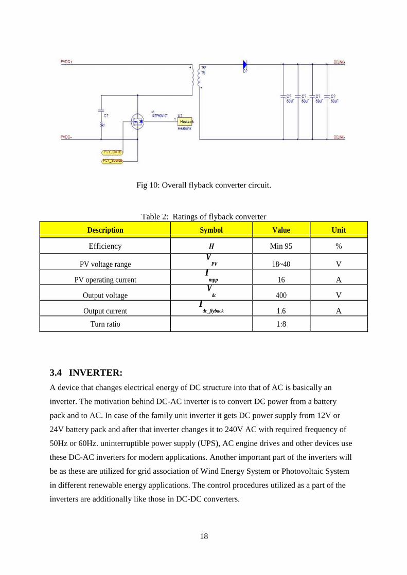
Fig 10: Overall flyback converter circuit.
Table 2: Ratings of flyback converter
Description Symbol Value Unit
Efficiency Η Min 95 %
PV voltage range V
PV 18~40 V
PV operating current I
mpp 16 A
Output voltage V
dc 400 V
Output current I
dc_flyback 1.6 A
Turn ratio 1:8
3.4 INVERTER:
A device that changes electrical energy of DC structure into that of AC is basically an
inverter. The motivation behind DC-AC inverter is to convert DC power from a battery
pack and to AC. In case of the family unit inverter it gets DC power supply from 12V or
24V battery pack and after that inverter changes it to 240V AC with required frequency of
50Hz or 60Hz. uninterruptible power supply (UPS), AC engine drives and other devices use
these DC-AC inverters for modern applications. Another important part of the inverters will
be as these are utilized for grid association of Wind Energy System or Photovoltaic System
in different renewable energy applications. The control procedures utilized as a part of the
inverters are additionally like those in DC-DC converters.
19
The DC-AC inverters more often than not work on Modulation of Pulse Width (PWM)
strategy. The Modulation of Pulse Width is an exceptionally advanced and valuable
method in which width of the Gate pulses will be done by different systems.To keep
the output voltage of the inverter at the required voltage (contingent upon the client's
decision) regardless of the output load PWM inverter is utilized. In normal inverter the
output voltage adjusts as per the changes in the load. To invalidate this impact of the
evolving loads. By changing the width of the pulses , the PWM inverter corrects the output
voltage and the switching frequency is the one output upon which AC relies.Pulse width is
balanced by estimation of the load joined at the output to give consistent output. The pulse
width regulated (PWM) mode is ordinary for inverter and change with circuit topologies,
which implies the nonlinearity of inverter, particularly smooth piecewise framework.
Notwithstanding this, the control techniques utilized as a part of the inverters are likewise
like those in DC-DC converters.
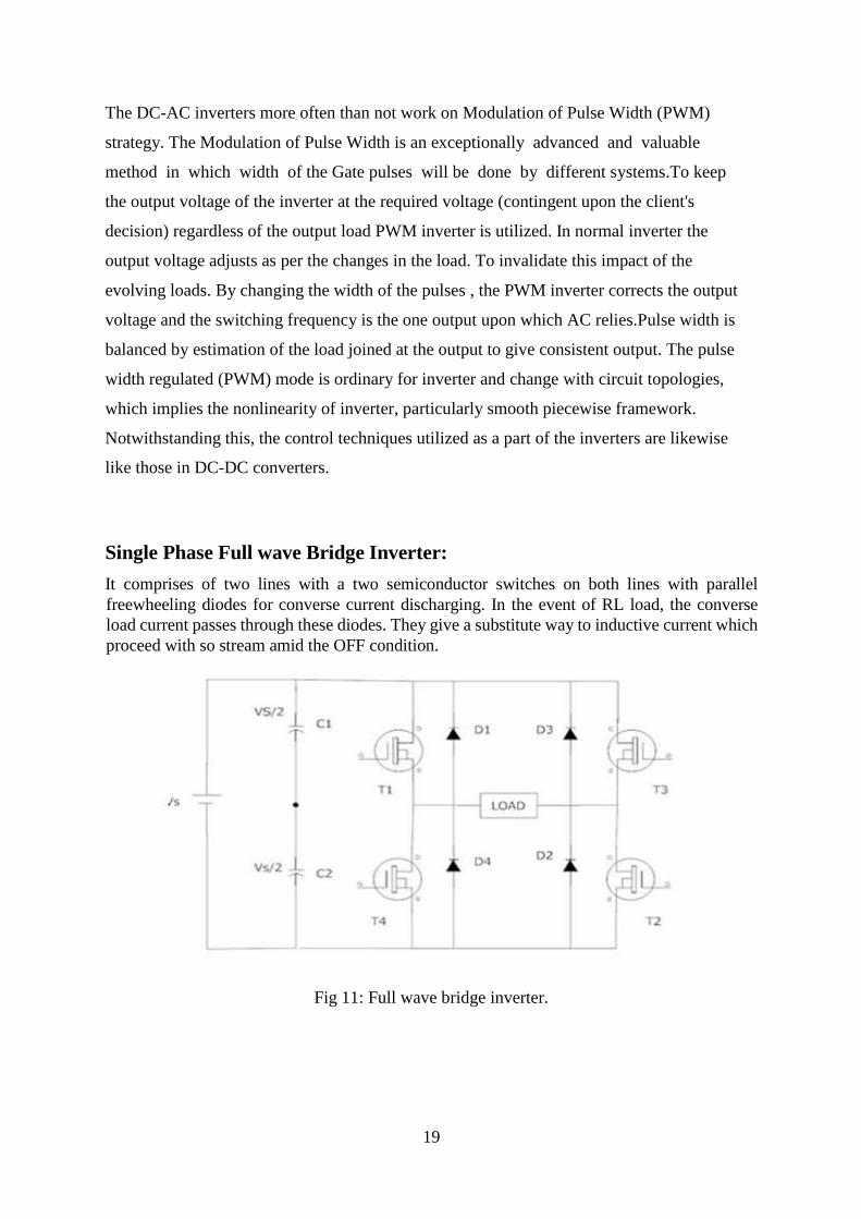
Single Phase Full wave Bridge Inverter:
It comprises of two lines with a two semiconductor switches on both lines with parallel
freewheeling diodes for converse current discharging. In the event of RL load, the converse
load current passes through these diodes. They give a substitute way to inductive current which
proceed with so stream amid the OFF condition.
Fig 11: Full wave bridge inverter.

20
Fig 12:On and Off conditions of thyristors in inverter.
T1, T2, T3 and T4 are the switches. The thyristors in every branch is worked then again
with the goal that they are not in same mode (ON/OFF) all the while. In reality they are both
OFF for a small time called blanking time, to evade short-circuiting. The T1 and T2
switches or T3 and T4 are supposed to work in a couple to get the output. These
extensionded legs are changed such that the output voltage shifts starting with one then onto
the next and later the adjustment in polarity happens in output-voltage waveform. The
output voltage zero, In the event that the shift angle is zero and when movement angle is π
output voltage is maximal.
3.5 Sinusoidal Pulse Width Modulation:
Sinusoidal PWM is a type of "carrier-based" pulse width modulation. Carrier based PWM
uses pre-defined modulation signals to determine output voltages. In sinusoidal PWM, the
modulation signal is sinusoidal, with the peak of the modulating signal always less than the
peak of the carrier signal. Sinusoidal PWM inverter leg and line-line voltages are illustrated
below.

21
Fig 13: sinusoidal pulse width modulation.
3.6 FILTER :
The harmonics due to pulsating modulation waveform can be reduced by connecting a low
pass filter to output side of Full Bridge voltage source inverter. The harmonics of low order
are removed by L-C filter. To work as a perfect source of voltage, even though the load may
be linear or non-linear load that gives no voltage variation, inverter’s impedance of output
should be kept zero. Consequently, the quality of capacitance ought to be augmented and
the inductance worth ought to be reduced by the low-pass filter at chosen cut-off frequency.
Every estimation of L and C segment is resolved such that reactive power is minimized in
these segments in light of the fact that the reactive power of L and C will be chosen such
that its expense is minimized, then the filter parts are dead set at a suitable low capacitance
and a high inductance and therefore the output impedance is very high. Under these
conditions the waveform of output voltage of inverter is sinusoidal under linear load and
output impedance is zero.
22
Fig 14: Inverter with LC filter.
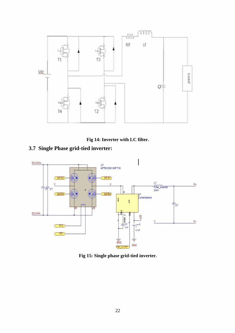
3.7 Single Phase grid-tied inverter:
Fig 15: Single phase grid-tied inverter.
23
Table 3: Specifications of inverter
3.8 GRID SYNCHRONISATION:
In a general structure distributed system, a power conversion unit converts input power into
electricity. The connection of generation station influences the electricity requirement of local
loads.
One important part of the distributed system is its control. The control tasks can be divided
into two major parts:
1. Input-side controller: Its main property is that it can extract the maximum power from
the input source. Naturally, protection of the input-side converter is also important to
be considered.
2. Grid – side controller: It performs the following:
a. It controls the active power generated
b. It controls the reactive power transfer between the DPGS and the grid
c. Control of the dc-link voltage is done by the grid-side controller
d. It ensures high quality of the injected power
The items listed above for the grid-side controller are the basic features this controller should
have. In addition to the above, auxiliary services like voltage harmonic compensation, active
filtering or local voltage and frequency regulation might be requested by the grid operator.

24
CHAPTER4
SIMULATION RESULTS

25
4.1 OVERALL SYSTEM DESCRIPTION:
Fig. 1 shows our overall design of microinverter. We have chosen a flyback converter topology
configuration on the front-end converter, because we need to not only boost voltage level but
also isolate from primary side to the secondary side for protection purpose. In addition, around
100~1kW power rating, a flyback converter has higher efficiency compared to the other
topologies. A snubber has been added to prevent spikes in voltage from switching, and a
current sensor has been added for additional protection of the components. The grid tied
inverter as a back-end converter will connect to the grid and transfer power as well. This will
then be synced with the grid in order to send power with respect to the grid voltage angle.
Filters are then used to get rid of the various noises associated with the system and meet the
harmonic suppression.
Fig16: overall configuration of system
4.2 FLYBACK CONVERTER:
Flyback converter side contains discrete MOSFET, RC snubber, high frequency transformer
and freewheeling diode. In order to do boosting and isolation, high frequency transformer is
adopted. Its turn ratio is 1:8. By using high frequency for switching the transient response
can improve with higher switching frequency and cost of converter gets reduced. So high
frequency of 40KHz is used for switching. PWM is generated PIC suite using PIC16F877A
microcontroller.

26
PIC code using PIC16F877A controller to generate 40KHz switching PWM for Flyback
converter:
void main() {
short duty1=128;
TRISD=0xFF;
TRISC=0;
pwm1_Init(40000);
pwm1_Start();
pwm1_set_duty(duty1);
while(1)
{
if(PORTD.F0==0)
{
delay_ms(1);
duty1++;
pwm1_set_duty(duty1);
}
if(PORTD.F1==0)
{
delay_ms(1);
duty1--;
pwm1_set_duty(duty1);
}
delay_ms(10);
}
}
Here duty1=(50*255)/100
Therefore duty1=128.

27
PWM of flyback converter:
Fig 17: PWM of 40KHz for Flyback converter.
Simulation model of Fly back converter in Proteus software:
Fig 18:Simulation model of Flyback converter in PROTEUS
Channel A Channel B Channel C Channel D 0

28
Fig 19: Output voltage of Flyback Converter.
4.3 INVERTER:
PIC code using PIC16F877A controller to generate 15KHz PWM for inverter:
void main() {
short duty1=128;
TRISD=0xFF;
TRISC=0;
pwm1_Init(15000);
pwm1_Start();
pwm1_set_duty(duty1);
while(1)
{
if(PORTD.F0==0)
{
delay_ms(1);
duty1++;
pwm1_set_duty(duty1);
}
if(PORTD.F1==0)

29
{
delay_ms(1);
duty1--;
pwm1_set_duty(duty1);
}
delay_ms(10);
}
}
Here duty1=(50*255)/100
Therefore duty1=128
PWM of inverter
Fig 20: PWM of 15KHz for inverter. Channel A Channel B Channel C Channel D
0

30
Simulation model of inverter in Proteus:
Fig 21: Simulation model of inverter in PROTEUS.
Output current waveform of inverter
Fig 22: Output current waveform of inverter. Channel A Channel B Channel C Channel D
0
31
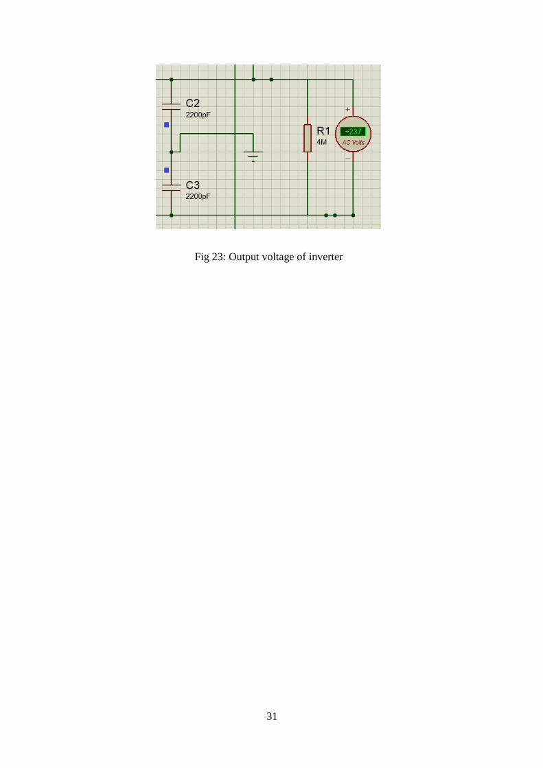
Fig 23: Output voltage of inverter

32
CHAPTER5
CONCLUSION
33
CONCLUSION:
The 18 to 40V voltage generated by PV array is stepped up to 400V DC voltage using a
Flyback converter with a switching frequency of 40KHz. Flyback converter is also used for
isolation purpose of primary to secondary sides. The 400V DC output voltage of Flyback
converter is converted to 240V AC voltage using inverter. The switching frequency of
inverter is 15KHz. Thus a 240V AC voltage is produced which can be directly used by loads.
REFERENCES:
[1]. Ming Li, Dong Dai & Xikui Ma, "Slow-Scale and Fast-Scale Instabilities in Voltage-
Mode Controlled Full-Bridge Inverter" Journal: Circuits Systems and Signal Processing -
CIRC SYST SIGNAL PROCESS , vol. 27, no. 6, pp. 811-831, 2008
[2]. Highly efficient grid-tied microinverter for photovoltaic panel
[3]. Calais M, Agelidis VG. Multilevel converters for single-phase grid connected
Photovoltaic systems Ð an overview. In: Proceedings of the IEEE International
Symposium on Industrial Electronics. Pretoria, South Africa, vol. 1, 1998, p. 224±9.
[4]. Martina Calaisa,*, Vassilios G. Agelidisb Michael S. Dymondc, “A cascaded inverter
for transformerless single-phase grid-connected photovoltaic systems, Renewable
Energy, volume 22, Issues 1-3, January - March 2011, page 255-262.
[5]. Hanju Cha and Trung-Kien Vu ,”Comparitive analysis of low pass output filter for
single- phase grid-connected photovoltaic inverter “,Department of Electrical
Engineering, Chungnam National University, Daejon, Korea.
[6]. R. Teodorescu, F. Blaabjerg, U. Borup, and M. Liserre, “A new control structure for grid-
connected LCL PV inverters with zero steady-state error and selective harmonic
compensation,” in Proc. IEEE APEC, 2004, vol. 1, pp. 580–586.
[7]. H. Zhu, B. Arnet, L. Haines, E. Shaffer, and J.-S. Lai, “Grid synchronization control
without ac voltage sensors,” in Proc. IEEE APEC, 2003,vol. 1, pp. 172–178.
[8]. "Small Photovoltaic Arrays”. Research Institute for Sustainable Energy (RISE), Murdoch
University. Retrieved 5 February 2010.
[9]. Welter P. Power up, prices down, grid connected inverter market survey (Leistung rauf,
Preise runter, MarkituÈ bersicht netzgekoppelter Wechselrichter, in German).
PHOTON-das Solarstrom Magizin (German Solar Electricity Magazine) 1999;3:48±57.
[10]. Solar Cells and their Applications Second Edition, Lewis Fraas, Larry Partain, Wiley,
2010,ISBN 978-0-470-44633-1, Section10.2.


