Download - Design of High Density Packaging IEEE

Package Science Services 1
Design of High Density & 3D Packaging: Tools and Knowledge
Thomas S. TarterPackage Science Services LLC
IEEE/CPMT Technical LuncheonSeptember 23, 2010

Package Science Services 2
Outline Package Design Flow (the old way) Package Design Flow (the right way) Evolution of Packaging Sciences Package Selection Moore’s Law, Miniaturization and Cost Chip Stacking and High-Density Designs Electrical Design and Analysis
Conclusion

Package Science Services 3
IC PACKAGING DESIGNFLOW
The Old Way

Package Science Services 4
DESIGN DEPT.NEW PROCESSOR
CHIP DESIGN
Our chip is finished! We have put 20 million transistors on an 8x10mm chip that runs at 3.5GHz and only dissipates 75 watts!

Package Science Services 5
Packaging Dept.
Now that we are done with our perfect chip, lets give it to the packaging crew!
!

Package Science Services 6
DESIGN DEPT.NEW PROCESSOR
CHIP DESIGN
All they have to do is get the heat out so it operates over 0 to 70°C ambient, make the 900 or so interconnects invisible to the electrical signals, make it robust enough to reliably operate for years and make the cost minimal. That should be easy!
Package Science Services 7
IC PACKAGING DESIGNFLOW
(The Right Way)

Package Science Services 8
Evolution of Packaging Science The old model of creating the device and then
packaging it is long gone Chip manufacturing has evolved to where simple, low-
performance designs can be packaged in the millions and billions with high yield and extremely low cost◦ This presents the illusion that all packaging is simple and
should be relatively easy and low cost Successful packaging of high technology devices
requires consideration at the outset of the device design◦ Concurrent design practices for the device and package are
mandatory for high performance products But the stigma remains

Package Science Services 9
21st CenturyHigh-Technology
Package
Chemistry MaterialsReliability
HeatTransfer
Mechanics
Electro-magneticsDigital /
AnalogEE
Metallo-graphy
SupplyChain
Manufacturing
Process
Design
HighFreq. /
RF
Layout /Routing
FailureAnalysis
21st CenturyHigh-Technology
Package
Chemistry MaterialsReliability
HeatTransfer
Mechanics
Electro-magneticsDigital /
AnalogEE
Metallo-graphy
SupplyChain
Manufacturing
Process
Design
HighFreq. /
RF
Layout /Routing
FailureAnalysis
IC Packaging Science Packaging of complex silicon devices requires a deep
knowledge of many aspects of high-technology engineering disciplines◦ As an example, packaging a high lead-count chip requires
knowledge of electrical, thermal, mechanical, chemical, reliability and materials engineering
◦ Taking the next step from prototype to mass-manufacture requires knowledge of manufacturing processes, materials, statistical methods (SPC), failure analysis and supply chain
These disciplines must be known and used in the conceptualization, design and implementation of any package design

Package Science Services 10
21st CenturyHigh-Technology
Package
Chemistry MaterialsReliability
HeatTransfer
Mechanics
Electro-magneticsDigital /
AnalogEE
Metallo-graphy
SupplyChain
Manufacturing
Process
Design
HighFreq. /
RF
Layout /Routing
FailureAnalysis

Package Science Services 11
Package Types Packaging has evolved with technology advances to meet
the needs of high-performance, low-cost and specialty designs
Selection of the best form factor must balance cost, performance and reliability
Form factors range from two-lead packages with simple structure to multi-layer, high-leadcount structures, stacked chips and package-on-package formats
Performance and I/O count have increased while the size of components and products have decreased◦ Drives the need for higher package integration◦ More functionality in a smaller space◦ Higher density and interconnectivity
Package Science Services 12
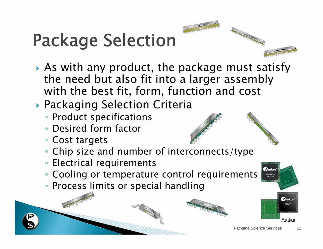
Package Selection As with any product, the package must satisfy
the need but also fit into a larger assembly with the best fit, form, function and cost
Packaging Selection Criteria◦ Product specifications◦ Desired form factor◦ Cost targets◦ Chip size and number of interconnects/type◦ Electrical requirements◦ Cooling or temperature control requirements◦ Process limits or special handling
AmkorAmkorAmkorAmkorAmkor

Package Science Services 13
Moore’s Law and packaging
The industry has been able to keep pace with Moore’s Law by shrinking transistors
3D packaging provides increased density and performance and is a key element to meeting/exceeding Moore’s predictions
Limitations to transistor gate size are an issue in the future and interconnect losses pose a serious problem for high speed chips now

Package Science Services 14
Miniaturization and Performance
High performance computing is limited by interconnect losses
Interconnect scalability cannot keep pace with gate length
Through-silicon vias help to reduce interconnect losses on-chip and chip-to-chip
Challenges include coupling and substrate interaction
Interconnect switching power can be 50% of overall dynamic power
Stacking chips can reduce chip-to-chip interconnect length but does not address on-chip interconnect length
Package Science Services 15
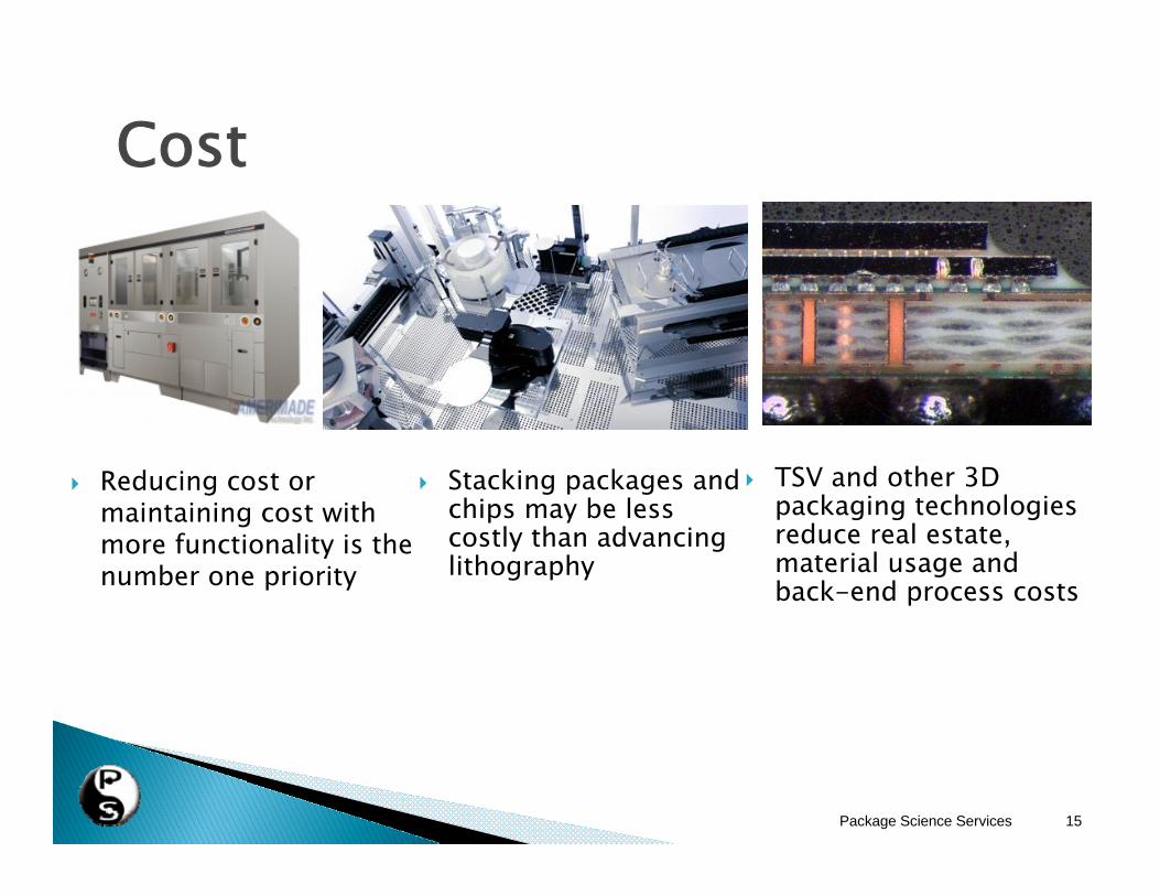
Cost
Reducing cost or maintaining cost with more functionality is the number one priority
TSV and other 3D packaging technologies reduce real estate, material usage and back-end process costs
Stacking packages and chips may be less costly than advancing lithography
Package Science Services 16
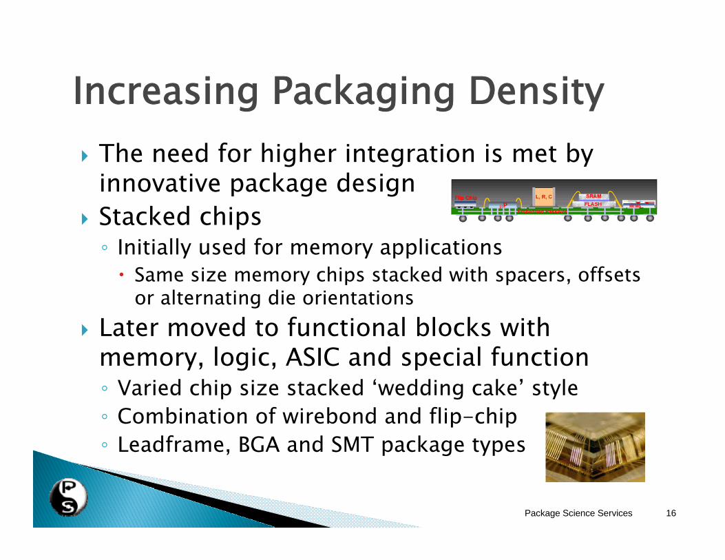
Increasing Packaging Density The need for higher integration is met by
innovative package design Stacked chips◦ Initially used for memory applications Same size memory chips stacked with spacers, offsets
or alternating die orientations Later moved to functional blocks with
memory, logic, ASIC and special function◦ Varied chip size stacked ‘wedding cake’ style◦ Combination of wirebond and flip-chip◦ Leadframe, BGA and SMT package types

Package Science Services 17
Stacked Packages In some cases, it is not practical or possible
to stack all chips that make up a system into the same package but the need for miniaturization and connectivity remains◦ Cases where KGD are not available or connectivity
for test is not practical or possible◦ Modules can be assembled with different devices
for varied functionality or product mix◦ Temperature or process sensitivity
Stacked packages meet these needs

Package Science Services 18
Chip Stacking Considerations Performance and interconnectivity are primary
concerns when designing a stacked package When using same-type die, connectivity is not simple,
but it is constrained When using multiple die to create a 3D system in
package, connectivity is complex and requires intelligent software assistance
Various combinations of die rotations, connections to the substrate and chip-to-chip are possible
At this time, traditional tools are used to perform this function, but it is not by any means automated

Package Science Services 19
Electrical Design and Analysis

Package Science Services 20
Electrical Design Flow
Specifications, Netlist,
Schematic, CAD/CAM
Pre-LayoutZo, timing, coupling, DC
Geometry, Materials,Design rules
Start
Layout / Routing
AC full wave analysisDC, power network,
decoupling
SimulationSSO, Channel, Transient AC
Compare to Specifications
OptionTest Vehicle
builds
Post-Layout
Pass?NO
YES
Design Review
First Article
Production
Approve Design

Package Science Services 21
Layout and Routing Challenges The designer must choose the best layout based on not
only connectivity, but also must consider electrical performance ◦ Wire bond length can become excessive in stacked designs,
increasing the parasitics in the transmission path◦ Frequency components of digital signals require transmission
line design and analysis for relatively short interconnects Differential pairs for high speed data transfer Multiple power supply decoupling Analog interconnects (sensitive or RF)
◦ Design constraints include materials, manufacturability and cost Concurrent trace, plane and via modeling must be
performed to assure proper signal and power integrity

Package Science Services 22
Connectivity and Circuit Analysis Toolsets for 3D design must create accurate
connectivity netlists and allow interaction with modeling and simulation tools◦ Connectivity from chip-to-chip, chip-to-substrate and substrate-
to-PCB must be maintained throughout the design cycle Traditional 2D design tools may require concatenation of netlists to
maintain proper connectivity Contain limited 3D information
◦ 3D tools must maintain connectivity while allowing substitutionsor changes in individual chip, interposer or package layout or position in the stack
◦ Interoperability Must be able to interact with other tools
Import/ Export from chip/package/PCB CAD/CAM design tools Direct export to 3D modeling and simulation tools Import results from analysis tools for optimization and DRC Export design layout data to manufacturing files

Package Science Services 23
Circuit Path Example - TSV

Package Science Services 24
Example of a 3D Design ToolCAD Design Software EPD
◦ Allows stacking of multiple substrates Substrates may be chip, interposer, package,
substrate, PCB◦ Stack interconnected by bump, pillar, TSV, ball… Creates a single composite substrate Design, simulation and optimization of the entire
assembly Each component in the stack can be extracted as a
single element Distributed collaborative design Sub-modeling, circuit simulation Manufacturing, CAD/CAM files

Package Science Services 25
EPD 3D Package Design Flow
DATA INPUT
OPTIMIZATIONMODELING
SIMULATIONANALYSIS
DATA OUTPUT

Package Science Services 26
EPD 3D Model of POP

Package Science Services 27
Data in, Data OutInteroperabilityModeling and Simulation

Package Science Services 28
System Interoperability
Q3DHFSS
SIWaveDesigner –Write Only
Microwave Studio – Write Only
PakSi-E – Write Only
ADS –Read / Write
IFFANF
MODSON
AutoCADAutoCAD MechanicalInventor Read / Write
Pro-E - Write Solid Edge Read / Write
IGES
STEPACIS
DWG
DXF
High Level Links
Low Level Links
•MCAD•CAE•Stress•Thermal
•Signal Integrity•Power Integrity•EM analysis•Channel Modeling and simulation (PCIe, SERDES..)
•EDA
SolidWorksCatiaACIS Modeler –Read / WriteAllegro/APD/SIP-
Read / Write
GDSGerber
IDF
BoardStation – Read OnlyExpedition – Read / WritePADS – Read / Write
CR5000 - Read OnlyPWS - Read OnlyBoard Designer – Read Only
IDF format – Read / Write
Specctra –Read / Write
IPC
Agilent
Write Only
Microwave Office Read only
AWR
VBS
Any PCB Tool –Read CAM and Intelligize
Si2
Read / Write
Write Only

Package Science Services 29
Tools Some commercial tools for electrical
modeling and analysis◦ FEM, FDTD, PEEC, MOM and other solution methods◦ Typically include internal or third-party circuit
generation and simulation engines◦ Output may be s-parameters, SPICE or HSPICE
circuits, lumped or distributed circuit models
Q3DHFSS
SiWaveDesigner
Microwave Studio
PakSi-E
Microwave Office
ADS

Package Science Services 30
Full-Wave Solution Examples of results from full-wave solvers E field in EMI study, E field results for coupled
transmission line
rTBW 5.035.0
Geometry Field Strength

Package Science Services 31
Plane Coupling and Discontinuities E-Systems SPHINX Signoff◦ Co-modeling and simulation of traces and planes◦ Multilayer Finite Difference Method◦ Extract frequency domain information, convert to circuit
model, simulate◦ Allows concurrent design and optimization Current/voltage distribution, decoupling requirements for
power networks Trace impedance, coupling from trace-to-trace, trace-to-
plane Effect of return path discontinuities (RPD) Inconsistent planes (gaps, holes) Layer-to-layer transition effects (vias, vertical connections)

Package Science Services 32
Multilayer Modeling Example Coupling of a trace through a void in a plane◦ Transmission paths are typically not ‘straight
through’ Changes in impedance due to gaps, voids, degassing
holes, layer changes and trace-to-trace and trace-to-plane distances, microstrip to stripline
◦ It is necessary to understand the effect of these aberrations in the signal path◦ Placement of decoupling elements

Package Science Services 33
0.4mm
0.4mm
Plane 1
Plane 2Plane 3
Port 1
Port 2
46mm
46mm
15x15mm
0.035mmCU
Port 3
0.4mm
Trace is:1.25mm wide25mm long
ER=4.0LossTan=0.02
Objective: Accurately CaptureCoupling through a Void in a Plane

Package Science Services 34
Port 1
Port 3
Coupling of Trace through Void

Package Science Services 35
Microstrip Line is0.17 x 30mm long
ER=4.0LossTan=0.02
30um
0.150Diameter vias
Microstrip Transition Case (RPD)

Package Science Services 36
Microstrip Transition Case (S21)
Port1 Port2
MeasurementSphinx

Package Science Services 37
Undesirable Couplinginto the plane neartransition point >10%at certain frequencies
..needs to be accounted for.
MeasurementSphinx
Microstrip Via Transition Coupling to a Plane

Package Science Services 38
Simulation Circuit models generated from s-parameter
or time-domain or both Circuit model topology determined Circuit model subjected to stimulation Frequency response, signal distortion, eye
diagram analysis SPICE, other simulation engines

Package Science Services 39
Simulation and Data Correlation AtaiTec ADK Advanced SI Design Kit◦ ADK is a toolkit which contains a multitude of tools
for signal analysis, data correlation and correction, 2D extraction tools and simulation engines

Package Science Services 40
Simulation Example (ADK)
Maximum positive = 0.224461 volt at t = 0.0064 nsMinimum negative = -0.21754 volt at t = 0.1584 nsMaximum eye height = 0.441001 volt at t = 0.1584 nsEye height = 0.440938 volt at t = 0Eye width = 0.109645 ns at greater than 0.1 volt p-pFuzz = 0.0356489 ns at 0 volt crossing

Package Science Services 41
LLboard3L=800 pH
RRboard3R=10 mOhm
LLboard2L=800 pH
RRboard2R=60 mOhm
RRboard1R=0.47 mOhm
CC1
LLboard_1L=230 pH
CC2
PortP1
PortP2
Circuit Topology and Results Circuit topology based on
physical structure and number of elements needed to accurately describe behavior
Optimize components and topology to obtain best fit
Chip Capacitor Equivalent CircuitDistributed model

Package Science Services 42
Timing and Signal Analysis
286mV
1.1ns
274mV
1.1ns
Measurement
Simulation

Package Science Services 43
Eye Diagram Analysis
Measurement Simulation

Package Science Services 44
System Level Modeling and Simulation
CHIP
Interconnect
PACKAGE
flip-chip,wirebond
S-parameter
ball, lead, pin
S-parameter
Interconnect
SOCKET
Interconnect
Traces, Vias, PlanesQ2D, HFSS, ADSS-parameter, RLC, Spice
PCB
CONNECTOR
Traces, Vias, PlanesS-parameter, RLC, Spice
ball, lead, pin
S-parameter
RCVR (DDR, MODULE)
RLC
RLC
EXAMPLE SIGNAL PATH
DIE
PACKAGE
SOCKET
BOARD
SOCKETPACKAGE VIA BOARD VIA
CONNECTOR
DDR / MODULE
DIE
PACKAGE
SOCKET
BOARD
SOCKETPACKAGE VIA BOARD VIA
CONNECTOR
DDR / MODULE
Interconnectand
Package
ball, lead, pin
S-parameter

Package Science Services 45
Conclusion High performance packaging requires many
disciplines to select, design, characterize and manufacture
Package design for high performance devices should be considered at the outset of chip design
Electrical signal and power integrity are key to successful packaging of high speed digital products
3D tools for modeling and simulation are evolving to meet the needs of stacked packages and vertical interconnect methods such as TSV
A series of lectures on measurement and modeling are planned for the future

Package Science Services 46
THANK YOU!
www.pkgscience.com
THANKS TO:
CAD Design Softwarewww.cad-design.com
E-System Designwww.e-systemdesign.com
AtaiTec Co.www.ataitec.com
ADK


