Download - Description Features - Farnell

1©2020 Renesas Electronics Corporation November 5, 2020
DescriptionThe 8V19N492 is a fully integrated FemtoClock NG jitter attenuator and clock synthesizer designed as a high-performance clock solution for conditioning and frequency/phase management of wireless base station radio equipment boards. The device is optimized to deliver excellent phase noise performance as required in GSM, WCDMA, LTE, and LTE-A radio board implementations. The device supports JESD204B subclass 0 and 1 clocks.
A two-stage PLL architecture supports both jitter attenuation and frequency multiplication. The first stage PLL is the jitter attenuator and uses an external VCXO for best possible phase noise characteristics. The second stage PLL locks on the VCXO-PLL output signal and synthesizes the target frequency.
The device supports the clock generation of high-frequency clocks from the selected VCO and low-frequency synchronization signals (SYSREF). SYSREF signals are internally synchronized to the clock signals. Delay functions exist for achieving alignment and controlled phase delay between system reference and clock signals and to align/delay individual output signals. The four redundant inputs are monitored for activity. Four selectable clock switching modes are provided to handle clock input failure scenarios. Auto-lock, individually programmable output frequency dividers, and phase adjustment capabilities are added for flexibility.
The device is configured through a three-wire SPI interface and reports lock and signal loss status in internal registers and via a lock detect (LOCK) output. Internal status bit changes can also be reported via the nINT output. The 8V19N492 is ideal for driving converter circuits in wireless infrastructure, radar/imaging, and instrumentation/medical applications. The device is a member of the high-performance clock family from Renesas.
Typical Applications Wireless infrastructure applications: GSM, WCDMA, LTE,
and LTE-A Ideal clock driver for jitter-sensitive ADC and DAC circuits Low phase noise clock generation Ethernet line cards Radar and imaging Instrumentation and medical
Features High-performance clock RF-PLL with support for JESD204B Optimized for low phase noise: -150dBc/Hz (800kHz offset;
245.76MHz clock) Integrated phase noise of 80fs RMS typical (12k-20MHz). Dual-PLL architecture 1st-PLL stage with external VCXO for clock jitter attenuation 2nd-PLL with internal FemtoClockNG PLL: 2949.12MHz Six output channels with a total of 16 outputs, organized in:
• Four JESD204B channels (device clock and SYSREF output) with two, four and five outputs
• One clock channel with two outputs• One VCXO output
Configurable integer clock frequency dividers Supported clock output frequencies include: 2949.12, 1474.56,
983.04, 491.52, 245.76, and 122.88MHz Low-power LVPECL/LVDS outputs support configurable signal
amplitude, DC and AC coupling and LVPECL, LVDS line terminations techniques
Phase delay circuits• Clock phase delay with 256 steps of 339ps and a range of
0 to 86.466ns• Individual SYSREF phase delay with 8 steps of 169ps• Additional individual SYSREF fine phase delay with 25ps
steps• Global SYSREF signal delay with 256 steps of 339ps and a
range of 0 to 86.466 ns Redundant input clock architecture with two inputs and
• Input activity monitoring• Manual and automatic, fault-triggered clock selection modes• Priority controlled clock selection• Digital holdover and hitless switching• Differential inputs accept LVDS and LVPECL signals
SYSREF generation modes include internal and external trigger mode for JESD204B
Supply voltage: 3.3V SPI and control I/O voltage: 1.8V/3.3V (Selectable) Package: 10 x 10 mm 88-VFQFPN Temperature range: -40°C to +105°C (Case)
8V19N492Datasheet
FemtoClock® NG Jitter Attenuator and Clock Synthesizer

2©2020 Renesas Electronics Corporation November 5, 2020
8V19N492 Datasheet
Block DiagramFigure 1. Block Diagram (fVCO = 2949.12MHz)
CLK_0nCLK_0
Clock Monitor
and Selector
PFDCP
÷MV0
C0
R0
C1
LFV
OSC
nOSC
fVCXO
PFDCP
÷PV
÷MF
Holdover
BYPV
SYSREF Generator
SPI
RegisterFile
÷NS
FemtoClockNG
fVCO
nINT
LOCK
SDAT
SCLK
nCS
x2
÷NA
ΦCLK_A
ΦREF_A0 MUX_A0
Channel A
QCLK_A[1:0]nQCLK_A[1:0]
2
MUX_A1ΦREF_A1
QREF_A0nQREF_A0
QREF_A1nQREF_A1
÷NB
ΦCLK_B
ΦREF_B0 MUX_B0
Channel B
QCLK_B[1:0]nQCLK_B[1:0]
2
MUX_B1ΦREF_B1
QREF_B0nQREF_B0
QREF_B1nQREF_B1
÷NC
ΦCLK_C
ΦREF_C MUX_CChannel C
QCLK_CnQCLK_C
QREF_CnQREF_C
÷ND
ΦCLK_D
ΦREF_D MUX_DChannel D
QCLK_DnQCLK_D
QREF_DnQREF_D
÷NE
ΦCLK_E
Channel E
QCLK_E0nQCLK_E0
QCLK_E1nQCLK_E1
EXT_SYS
BYPF
÷MV1
ΦREF_S
QCLK_VnQCLK_V
SELSV
FDF÷PFCLK_1
nCLK_1
QREF_A2nQREF_A2
ΦREF_A2
C2
R1
C3
ICPF
LFF
LFFR
CR
CR
FemtoClockNG PLL Loop Filter
VCXO-PLL Loop Filter
MUX_A2
VDD_LCF

3©2020 Renesas Electronics Corporation November 5, 2020
8V19N492 Datasheet
ContentsDescription . . . . . . . . . . . . . . . . . . . . . . . . . . . . . . . . . . . . . . . . . . . . . . . . . . . . . . . . . . . . . . . . . . . . . . . . . . . . . . . . . . . . . . . . . . . . . . . . . . . . . . 1Typical Applications . . . . . . . . . . . . . . . . . . . . . . . . . . . . . . . . . . . . . . . . . . . . . . . . . . . . . . . . . . . . . . . . . . . . . . . . . . . . . . . . . . . . . . . . . . . . . . . 1Features . . . . . . . . . . . . . . . . . . . . . . . . . . . . . . . . . . . . . . . . . . . . . . . . . . . . . . . . . . . . . . . . . . . . . . . . . . . . . . . . . . . . . . . . . . . . . . . . . . . . . . . . 1Block Diagram . . . . . . . . . . . . . . . . . . . . . . . . . . . . . . . . . . . . . . . . . . . . . . . . . . . . . . . . . . . . . . . . . . . . . . . . . . . . . . . . . . . . . . . . . . . . . . . . . . . 2Pin Assignments. . . . . . . . . . . . . . . . . . . . . . . . . . . . . . . . . . . . . . . . . . . . . . . . . . . . . . . . . . . . . . . . . . . . . . . . . . . . . . . . . . . . . . . . . . . . . . . . . . 5Pin Descriptions . . . . . . . . . . . . . . . . . . . . . . . . . . . . . . . . . . . . . . . . . . . . . . . . . . . . . . . . . . . . . . . . . . . . . . . . . . . . . . . . . . . . . . . . . . . . . . . . . . 6Principles of Operation . . . . . . . . . . . . . . . . . . . . . . . . . . . . . . . . . . . . . . . . . . . . . . . . . . . . . . . . . . . . . . . . . . . . . . . . . . . . . . . . . . . . . . . . . . . . . 8
Overview . . . . . . . . . . . . . . . . . . . . . . . . . . . . . . . . . . . . . . . . . . . . . . . . . . . . . . . . . . . . . . . . . . . . . . . . . . . . . . . . . . . . . . . . . . . . . . . . . . . 8Phase-Locked Loop Operation . . . . . . . . . . . . . . . . . . . . . . . . . . . . . . . . . . . . . . . . . . . . . . . . . . . . . . . . . . . . . . . . . . . . . . . . . . . . . . . . . . 9
Frequency Generation . . . . . . . . . . . . . . . . . . . . . . . . . . . . . . . . . . . . . . . . . . . . . . . . . . . . . . . . . . . . . . . . . . . . . . . . . . . . . . . . . . . . 9VCXO-PLL . . . . . . . . . . . . . . . . . . . . . . . . . . . . . . . . . . . . . . . . . . . . . . . . . . . . . . . . . . . . . . . . . . . . . . . . . . . . . . . . . . . . . . . . . . . . 10FemtoClockNG PLL . . . . . . . . . . . . . . . . . . . . . . . . . . . . . . . . . . . . . . . . . . . . . . . . . . . . . . . . . . . . . . . . . . . . . . . . . . . . . . . . . . . . . 11
Channel Frequency Divider . . . . . . . . . . . . . . . . . . . . . . . . . . . . . . . . . . . . . . . . . . . . . . . . . . . . . . . . . . . . . . . . . . . . . . . . . . . . . . . . . . . . 12Redundant Inputs . . . . . . . . . . . . . . . . . . . . . . . . . . . . . . . . . . . . . . . . . . . . . . . . . . . . . . . . . . . . . . . . . . . . . . . . . . . . . . . . . . . . . . . . . . . 13
Monitoring and LOS of Input Signal . . . . . . . . . . . . . . . . . . . . . . . . . . . . . . . . . . . . . . . . . . . . . . . . . . . . . . . . . . . . . . . . . . . . . . . . . 13Input Re-Validation . . . . . . . . . . . . . . . . . . . . . . . . . . . . . . . . . . . . . . . . . . . . . . . . . . . . . . . . . . . . . . . . . . . . . . . . . . . . . . . . . . . . . . 13Clock Selection . . . . . . . . . . . . . . . . . . . . . . . . . . . . . . . . . . . . . . . . . . . . . . . . . . . . . . . . . . . . . . . . . . . . . . . . . . . . . . . . . . . . . . . . . 14Holdover . . . . . . . . . . . . . . . . . . . . . . . . . . . . . . . . . . . . . . . . . . . . . . . . . . . . . . . . . . . . . . . . . . . . . . . . . . . . . . . . . . . . . . . . . . . . . . 14Input Priorities . . . . . . . . . . . . . . . . . . . . . . . . . . . . . . . . . . . . . . . . . . . . . . . . . . . . . . . . . . . . . . . . . . . . . . . . . . . . . . . . . . . . . . . . . . 14Hold-off Counter . . . . . . . . . . . . . . . . . . . . . . . . . . . . . . . . . . . . . . . . . . . . . . . . . . . . . . . . . . . . . . . . . . . . . . . . . . . . . . . . . . . . . . . . 15
Revertive Switching . . . . . . . . . . . . . . . . . . . . . . . . . . . . . . . . . . . . . . . . . . . . . . . . . . . . . . . . . . . . . . . . . . . . . . . . . . . . . . . . . . . . . . . . . . 15Short-Term Holdover . . . . . . . . . . . . . . . . . . . . . . . . . . . . . . . . . . . . . . . . . . . . . . . . . . . . . . . . . . . . . . . . . . . . . . . . . . . . . . . . . . . . . . . . . 15
Automatic with Holdover (nM/A[1:0] = 11) . . . . . . . . . . . . . . . . . . . . . . . . . . . . . . . . . . . . . . . . . . . . . . . . . . . . . . . . . . . . . . . . . . . . 15VCXO-PLL Lock Detect . . . . . . . . . . . . . . . . . . . . . . . . . . . . . . . . . . . . . . . . . . . . . . . . . . . . . . . . . . . . . . . . . . . . . . . . . . . . . . . . . . 16FemtoClockNG Loss-of-Lock (LOLF) . . . . . . . . . . . . . . . . . . . . . . . . . . . . . . . . . . . . . . . . . . . . . . . . . . . . . . . . . . . . . . . . . . . . . . . . 17
Channel, Output, and JESD204B Logic . . . . . . . . . . . . . . . . . . . . . . . . . . . . . . . . . . . . . . . . . . . . . . . . . . . . . . . . . . . . . . . . . . . . . . . . . . 18Channel . . . . . . . . . . . . . . . . . . . . . . . . . . . . . . . . . . . . . . . . . . . . . . . . . . . . . . . . . . . . . . . . . . . . . . . . . . . . . . . . . . . . . . . . . . . . . . 18
Differential Outputs . . . . . . . . . . . . . . . . . . . . . . . . . . . . . . . . . . . . . . . . . . . . . . . . . . . . . . . . . . . . . . . . . . . . . . . . . . . . . . . . . . . . . . . . . . 18Output Phase Delay . . . . . . . . . . . . . . . . . . . . . . . . . . . . . . . . . . . . . . . . . . . . . . . . . . . . . . . . . . . . . . . . . . . . . . . . . . . . . . . . . . . . . . . . . 21Configuration for JESD204B Operation . . . . . . . . . . . . . . . . . . . . . . . . . . . . . . . . . . . . . . . . . . . . . . . . . . . . . . . . . . . . . . . . . . . . . . . . . . 21
Synchronizing SYSREF and Clock Output Dividers . . . . . . . . . . . . . . . . . . . . . . . . . . . . . . . . . . . . . . . . . . . . . . . . . . . . . . . . . . . . . 21SYSREF Generation . . . . . . . . . . . . . . . . . . . . . . . . . . . . . . . . . . . . . . . . . . . . . . . . . . . . . . . . . . . . . . . . . . . . . . . . . . . . . . . . . . . . . 21Internal SYSREF Generation . . . . . . . . . . . . . . . . . . . . . . . . . . . . . . . . . . . . . . . . . . . . . . . . . . . . . . . . . . . . . . . . . . . . . . . . . . . . . . 23External SYSREF Generation . . . . . . . . . . . . . . . . . . . . . . . . . . . . . . . . . . . . . . . . . . . . . . . . . . . . . . . . . . . . . . . . . . . . . . . . . . . . . 23QCLK to QREF (SYSREF) Phase Alignment . . . . . . . . . . . . . . . . . . . . . . . . . . . . . . . . . . . . . . . . . . . . . . . . . . . . . . . . . . . . . . . . . . 23
Deterministic Phase Relationship and Phase Alignment . . . . . . . . . . . . . . . . . . . . . . . . . . . . . . . . . . . . . . . . . . . . . . . . . . . . . . . . . . . . . 24Status Conditions and Interrupts . . . . . . . . . . . . . . . . . . . . . . . . . . . . . . . . . . . . . . . . . . . . . . . . . . . . . . . . . . . . . . . . . . . . . . . . . . . . . . . . 25Device Startup, Reset, and Synchronization . . . . . . . . . . . . . . . . . . . . . . . . . . . . . . . . . . . . . . . . . . . . . . . . . . . . . . . . . . . . . . . . . . . . . . . 26
Recommended Configuration Sequence (In Order): . . . . . . . . . . . . . . . . . . . . . . . . . . . . . . . . . . . . . . . . . . . . . . . . . . . . . . . . . . . . 26Changing Frequency Dividers and Phase Delay Values . . . . . . . . . . . . . . . . . . . . . . . . . . . . . . . . . . . . . . . . . . . . . . . . . . . . . . . . . 27
SPI Interface . . . . . . . . . . . . . . . . . . . . . . . . . . . . . . . . . . . . . . . . . . . . . . . . . . . . . . . . . . . . . . . . . . . . . . . . . . . . . . . . . . . . . . . . . . . . . . . 27Configuration Registers . . . . . . . . . . . . . . . . . . . . . . . . . . . . . . . . . . . . . . . . . . . . . . . . . . . . . . . . . . . . . . . . . . . . . . . . . . . . . . . . . . . . . . . . . . . 30
Channel and Clock Output Registers . . . . . . . . . . . . . . . . . . . . . . . . . . . . . . . . . . . . . . . . . . . . . . . . . . . . . . . . . . . . . . . . . . . . . . . . . . . . 33QREF Output State Registers . . . . . . . . . . . . . . . . . . . . . . . . . . . . . . . . . . . . . . . . . . . . . . . . . . . . . . . . . . . . . . . . . . . . . . . . . . . . . . . . . . 35PLL Frequency Divider Registers . . . . . . . . . . . . . . . . . . . . . . . . . . . . . . . . . . . . . . . . . . . . . . . . . . . . . . . . . . . . . . . . . . . . . . . . . . . . . . 38VCXO-PLL Control Registers . . . . . . . . . . . . . . . . . . . . . . . . . . . . . . . . . . . . . . . . . . . . . . . . . . . . . . . . . . . . . . . . . . . . . . . . . . . . . . . . . . 40Input Selection Mode Registers . . . . . . . . . . . . . . . . . . . . . . . . . . . . . . . . . . . . . . . . . . . . . . . . . . . . . . . . . . . . . . . . . . . . . . . . . . . . . . . . 42SYSREF Control Registers . . . . . . . . . . . . . . . . . . . . . . . . . . . . . . . . . . . . . . . . . . . . . . . . . . . . . . . . . . . . . . . . . . . . . . . . . . . . . . . . . . . 45

4©2020 Renesas Electronics Corporation November 5, 2020
8V19N492 Datasheet
Status Registers . . . . . . . . . . . . . . . . . . . . . . . . . . . . . . . . . . . . . . . . . . . . . . . . . . . . . . . . . . . . . . . . . . . . . . . . . . . . . . . . . . . . . . . . . . . . 47General Control Registers . . . . . . . . . . . . . . . . . . . . . . . . . . . . . . . . . . . . . . . . . . . . . . . . . . . . . . . . . . . . . . . . . . . . . . . . . . . . . . . . . . . . 50
Absolute Maximum Ratings . . . . . . . . . . . . . . . . . . . . . . . . . . . . . . . . . . . . . . . . . . . . . . . . . . . . . . . . . . . . . . . . . . . . . . . . . . . . . . . . . . . . . . . . 51Pin Characteristics . . . . . . . . . . . . . . . . . . . . . . . . . . . . . . . . . . . . . . . . . . . . . . . . . . . . . . . . . . . . . . . . . . . . . . . . . . . . . . . . . . . . . . . . . . . . . . . 52DC Characteristics . . . . . . . . . . . . . . . . . . . . . . . . . . . . . . . . . . . . . . . . . . . . . . . . . . . . . . . . . . . . . . . . . . . . . . . . . . . . . . . . . . . . . . . . . . . . . . . 52AC Characteristics . . . . . . . . . . . . . . . . . . . . . . . . . . . . . . . . . . . . . . . . . . . . . . . . . . . . . . . . . . . . . . . . . . . . . . . . . . . . . . . . . . . . . . . . . . . . . . . 56
Clock Phase Noise Characteristics . . . . . . . . . . . . . . . . . . . . . . . . . . . . . . . . . . . . . . . . . . . . . . . . . . . . . . . . . . . . . . . . . . . . . . . . . . . . . . 63Application Information. . . . . . . . . . . . . . . . . . . . . . . . . . . . . . . . . . . . . . . . . . . . . . . . . . . . . . . . . . . . . . . . . . . . . . . . . . . . . . . . . . . . . . . . . . . . 67
Termination for QCLK_y, QREF_r LVDS Outputs (STYLE = 0) . . . . . . . . . . . . . . . . . . . . . . . . . . . . . . . . . . . . . . . . . . . . . . . . . . . . . . . . 67AC Termination for QCLK_y, QREF_r LVDS Outputs (STYLE = 0) . . . . . . . . . . . . . . . . . . . . . . . . . . . . . . . . . . . . . . . . . . . . . . . . . . . . . 67Termination for QCLK_y, QREF_r LVPECL Outputs (STYLE = 1) . . . . . . . . . . . . . . . . . . . . . . . . . . . . . . . . . . . . . . . . . . . . . . . . . . . . . . 68
Thermal Characteristics . . . . . . . . . . . . . . . . . . . . . . . . . . . . . . . . . . . . . . . . . . . . . . . . . . . . . . . . . . . . . . . . . . . . . . . . . . . . . . . . . . . . . . . . . . . 68Package Exposed Pad Thermal Release Path . . . . . . . . . . . . . . . . . . . . . . . . . . . . . . . . . . . . . . . . . . . . . . . . . . . . . . . . . . . . . . . . . . . . . 68Thermal Characteristics . . . . . . . . . . . . . . . . . . . . . . . . . . . . . . . . . . . . . . . . . . . . . . . . . . . . . . . . . . . . . . . . . . . . . . . . . . . . . . . . . . . . . . 69
Case Temperature Considerations . . . . . . . . . . . . . . . . . . . . . . . . . . . . . . . . . . . . . . . . . . . . . . . . . . . . . . . . . . . . . . . . . . . . . . . . . . 69Recommended Application Schematics . . . . . . . . . . . . . . . . . . . . . . . . . . . . . . . . . . . . . . . . . . . . . . . . . . . . . . . . . . . . . . . . . . . . . . . . . . 70
Package Outline Drawings . . . . . . . . . . . . . . . . . . . . . . . . . . . . . . . . . . . . . . . . . . . . . . . . . . . . . . . . . . . . . . . . . . . . . . . . . . . . . . . . . . . . . . . . . 72Marking Diagram . . . . . . . . . . . . . . . . . . . . . . . . . . . . . . . . . . . . . . . . . . . . . . . . . . . . . . . . . . . . . . . . . . . . . . . . . . . . . . . . . . . . . . . . . . . . . . . . 73Ordering Information . . . . . . . . . . . . . . . . . . . . . . . . . . . . . . . . . . . . . . . . . . . . . . . . . . . . . . . . . . . . . . . . . . . . . . . . . . . . . . . . . . . . . . . . . . . . . 73Glossary . . . . . . . . . . . . . . . . . . . . . . . . . . . . . . . . . . . . . . . . . . . . . . . . . . . . . . . . . . . . . . . . . . . . . . . . . . . . . . . . . . . . . . . . . . . . . . . . . . . . . . . 74Revision History . . . . . . . . . . . . . . . . . . . . . . . . . . . . . . . . . . . . . . . . . . . . . . . . . . . . . . . . . . . . . . . . . . . . . . . . . . . . . . . . . . . . . . . . . . . . . . . . . 74

5©2020 Renesas Electronics Corporation November 5, 2020
8V19N492 Datasheet
Pin AssignmentsFigure 2. Pinout for 10 x 10 mm, 88-VFQFPN Package with Exposed Pad (Top View)
Exposed Pad(GND)
VDD
_QCL
KD
nQ
RE
F_D
VDD
_QRE
FD
QR
EF_D
QCL
K_D
nQCL
K_D
VDD_
SYN
C
VDD_
LCV1
CLD
O
ICP
F
DN
U
DNU
CBIA
S
VDD_
LCV2 CR
LFFR LF
F
VDD
_LC
F
DNU
DNU
VDD
_CP
F
1
2
3
4
5
6
7
8
9
10
11
12
13
14
15
16
17
18
19
20
21
22
88 87 86 85 84 83 82 81 80 79 78 77 76 75 74 73 72 71 70 69 68 67
23 24 25 26 27 28 29 30 31 32 33 34 35 36 37 38 39 40 41 42 43 44
66
65
64
63
62
61
60
59
58
57
56
55
54
53
52
51
50
49
48
47
46
45
nQCLK_E1
QCLK_E0
VDD_QREFA2
VDD_QCLKA
nQREF_A0
VDD_QREFA0
VDD_QCLKE
QCLK_E1
nQCLK_E0
VDD_QCLKE
VDD_QREFA1
QREF_A1
nQREF_A1
QREF_A0
QCLK_A1
nQCLK_A1
QCLK_A0
nQCLK_A0
QREF_A2
nQREF_A2
VDD_QREFA2
VDD_QCLKA
VDD
_SPI
QCL
K_V
nCLK
_1
CLK
_0
nCLK
_0
VDD_
INP
VDD_
CPV
LFV
RES
_CAL
CLK
_1
nQC
LK_V
OSC
nOSC
VDD_
QC
LKV
SDAT
nIN
T
LOC
K
VDD_
QC
LKV
EXT_
SYS
nCS
SCLK
SELS
V
DNU
VDD_QREFB0
QREF_B0
nQREF_B0
QREF_B1
nQREF_B1
VDD_QREFB1
VDD_QCLKB
VDD_QCLKB
QCLK_B0
nQCLK_B0
QCLK_B1
nQCLK_B1
VDD_QREFC
QREF_C
nQREF_C
VDD_QREFC
VDD_QCLKC
QCLKC
nQCLK_C
VDD_QCLKC
DNU
VDD
_LC
F
6©2020 Renesas Electronics Corporation November 5, 2020
8V19N492 Datasheet
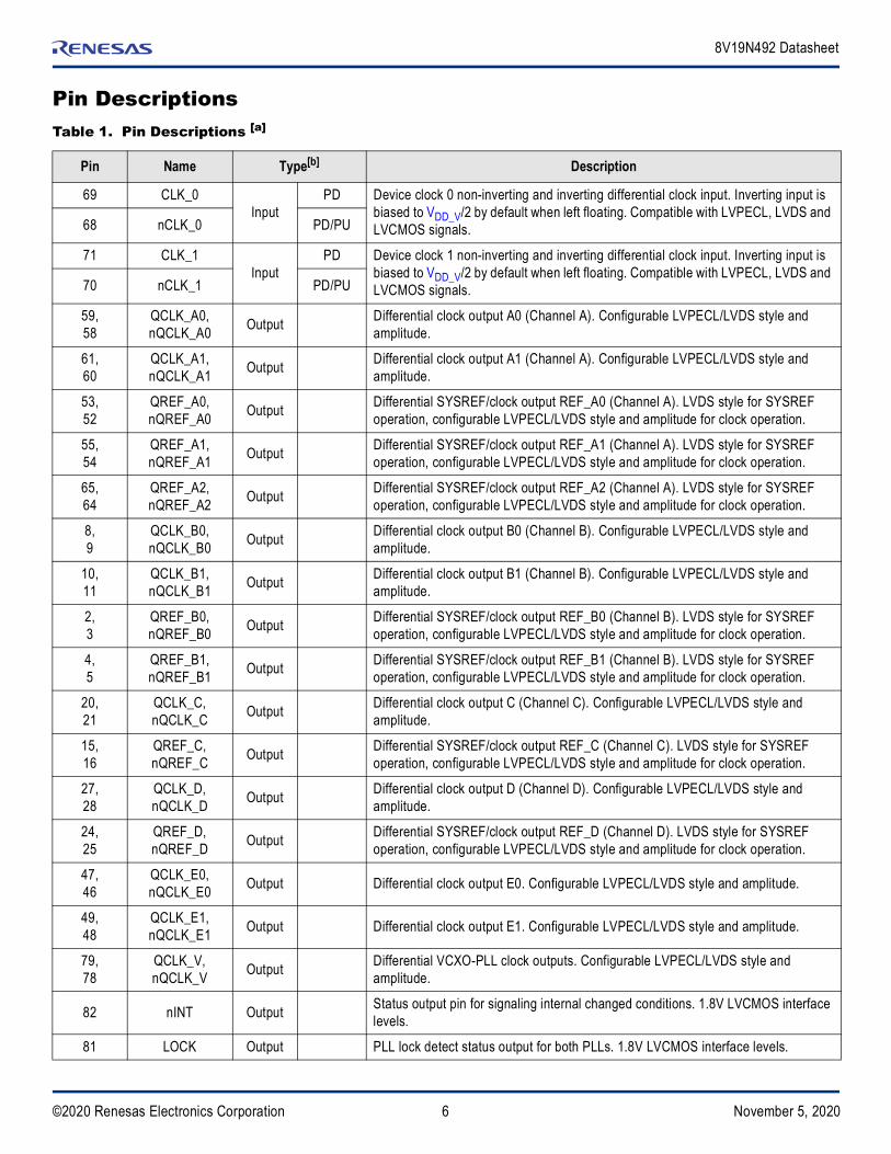
Pin DescriptionsTable 1. Pin Descriptions [a]
Pin Name Type[b] Description
69 CLK_0Input
PD Device clock 0 non-inverting and inverting differential clock input. Inverting input is biased to VDD_V/2 by default when left floating. Compatible with LVPECL, LVDS and LVCMOS signals.68 nCLK_0 PD/PU
71 CLK_1Input
PD Device clock 1 non-inverting and inverting differential clock input. Inverting input is biased to VDD_V/2 by default when left floating. Compatible with LVPECL, LVDS and LVCMOS signals.70 nCLK_1 PD/PU
59,58
QCLK_A0,nQCLK_A0 Output Differential clock output A0 (Channel A). Configurable LVPECL/LVDS style and
amplitude.
61,60
QCLK_A1,nQCLK_A1 Output Differential clock output A1 (Channel A). Configurable LVPECL/LVDS style and
amplitude.
53,52
QREF_A0, nQREF_A0 Output Differential SYSREF/clock output REF_A0 (Channel A). LVDS style for SYSREF
operation, configurable LVPECL/LVDS style and amplitude for clock operation.
55,54
QREF_A1, nQREF_A1 Output Differential SYSREF/clock output REF_A1 (Channel A). LVDS style for SYSREF
operation, configurable LVPECL/LVDS style and amplitude for clock operation.
65,64
QREF_A2, nQREF_A2 Output Differential SYSREF/clock output REF_A2 (Channel A). LVDS style for SYSREF
operation, configurable LVPECL/LVDS style and amplitude for clock operation.
8,9
QCLK_B0,nQCLK_B0 Output Differential clock output B0 (Channel B). Configurable LVPECL/LVDS style and
amplitude.
10,11
QCLK_B1,nQCLK_B1 Output Differential clock output B1 (Channel B). Configurable LVPECL/LVDS style and
amplitude.
2,3
QREF_B0, nQREF_B0 Output Differential SYSREF/clock output REF_B0 (Channel B). LVDS style for SYSREF
operation, configurable LVPECL/LVDS style and amplitude for clock operation.
4,5
QREF_B1, nQREF_B1 Output Differential SYSREF/clock output REF_B1 (Channel B). LVDS style for SYSREF
operation, configurable LVPECL/LVDS style and amplitude for clock operation.
20,21
QCLK_C,nQCLK_C Output Differential clock output C (Channel C). Configurable LVPECL/LVDS style and
amplitude.
15,16
QREF_C, nQREF_C Output Differential SYSREF/clock output REF_C (Channel C). LVDS style for SYSREF
operation, configurable LVPECL/LVDS style and amplitude for clock operation.
27,28
QCLK_D,nQCLK_D Output Differential clock output D (Channel D). Configurable LVPECL/LVDS style and
amplitude.
24,25
QREF_D, nQREF_D Output Differential SYSREF/clock output REF_D (Channel D). LVDS style for SYSREF
operation, configurable LVPECL/LVDS style and amplitude for clock operation.
47,46
QCLK_E0,nQCLK_E0 Output Differential clock output E0. Configurable LVPECL/LVDS style and amplitude.
49,48
QCLK_E1,nQCLK_E1 Output Differential clock output E1. Configurable LVPECL/LVDS style and amplitude.
79,78
QCLK_V,nQCLK_V Output Differential VCXO-PLL clock outputs. Configurable LVPECL/LVDS style and
amplitude.
82 nINT Output Status output pin for signaling internal changed conditions. 1.8V LVCMOS interface levels.
81 LOCK Output PLL lock detect status output for both PLLs. 1.8V LVCMOS interface levels.

7©2020 Renesas Electronics Corporation November 5, 2020
8V19N492 Datasheet
87 EXT_SYS Input PD External SYSREF pulse trigger input. 1.8V LVCMOS interface levels.
83 SDAT Input/Output PU Serial Control Port SPI Mode Clock Input and Output. Selectable 1.8V/3.3V
LVCMOS interface levels. 3.3V tolerant when set to 1.8V and set to input.
85 SCLK Input PD Serial Control Port SPI Mode Clock Input. Selectable 1.8V/3.3V LVCMOS interface levels. 3.3V tolerant when set to 1.8V.
86 nCS Input PU Serial Control Port SPI Chip Select Input. Selectable 1.8V/3.3V LVCMOS interface levels. 3.3V tolerant when set to 1.8V.
84 SELSV Input PD SPI interface voltage select. 1.8V LVCMOS interface levels (see Table 25 for SPI interface selection).
35 CR Analog Internal VCO regulator bypass capacitor. Use a 1.0μF capacitor between the CR and VDD_LCF pins.
33 CBIAS Analog Internal bias circuit for VCO. Connect a 4.7µF capacitor to GND.
36 CLDO Analog Internal LDO bypass for VCO. Connect a 10µF capacitor to GND.
73 LFV Output VCXO-PLL charge pump output. Connect to the loop filter for the external VCXO.
77 OSCInput
PD VCXO non-inverting and inverting differential clock input. Inverting input is biased to VDD_V /2 by default when left floating. Compatible with LVPECL, LVDS and LVCMOS signals.76 nOSC PD/PU
44 ICPF Analog Connect to LFF pin (38) and external loop filter.
38 LFF Output Loop filter/charge pump output for the FemtoClockNG NG PLL. Connect to the external loop filter.
37 LFFR Analog Ground return path pin for the VCO loop filter.
72 RES_CAL Analog Connect a 2.8 k (1%) resistor to GND for output current calibration.
13, 18, 23, 32, 41, 42 DNU Do not use, do not connect.
57, 62 VDD_QCLKA Power Positive supply voltage (3.3V) for the QCLK_A[1:0] outputs.
51 VDD_QREFA0 Power Positive supply voltage (3.3V) for the QREF_A0 outputs.
56 VDD_QREFA1 Power Positive supply voltage (3.3V) for the QREF_A1 outputs.
63, 66 VDD_QREFA2 Power Positive supply voltage (3.3V) for the QREF_A2 outputs.
7, 12 VDD_QCLKB Power Positive supply voltage (3.3V) for the QCLK_B[1:0] outputs.
1 VDD_QREFB0 Power Positive supply voltage (3.3V) for the QREF_B0 output.
6 VDD_QREFB1 Power Positive supply voltage (3.3V) for the QREF_B1 output.
19, 22 VDD_QCLKC Power Positive supply voltage (3.3V) for the QCLK_C outputs.
14, 17 VDD_QREFC Power Positive supply voltage (3.3V) for the QREF_C outputs.
29 VDD_QCLKD Power Positive supply voltage (3.3V) for the QCLK_D outputs.
26 VDD_QREFD Power Positive supply voltage (3.3V) for the QREF_D outputs.
45, 50 VDD_QCLKE Power Positive supply voltage (3.3V) for the QCLK_E[1:0] outputs.
88 VDD_SPI Power Positive supply voltage (3.3V) for the SPI interface.
67 VDD_INP Power Positive supply voltage (3.3V) for the differential inputs (CLK0 to CLK1).
Table 1. Pin Descriptions (Cont.)[a]
Pin Name Type[b] Description

8©2020 Renesas Electronics Corporation November 5, 2020
8V19N492 Datasheet
Principles of Operation
OverviewThe 8V19N492 generates low-phase noise, synchronized clock and SYSREF output signals locked to an input reference frequency. The device contains two PLLs with configurable frequency dividers. The first PLL (VCXO-PLL, suffix V) uses an external VCXO as the oscillator and provides jitter attenuation. The external loop filter is used to set the VCXO-PLL bandwidth frequency in conjunction with internal parameters. The second, low-phase noise PLL (FemtoClock NG, suffix F) multiplies the VCXO-PL1L frequency to 2949.12MHz. The FemtoClock NG PLL is completely internal and provides a central timing reference point for all output signals. From this point, fully synchronous dividers generate the output frequencies and the internal timing references for JESD204B support.
The device supports the generation of SYSREF pulses synchronous to the clock signals. There are five channels consisting of clock and/or SYSREF outputs. The clock outputs are configurable with support for LVPECL or LVDS formats and a variable output amplitude. Clock and SYSREF offer adjustable phase delay functionality. Individual outputs and channels and unused circuit blocks support powered-down states for operating at lower power consumption. The register map, accessible through SPI interface with read-back capability controls the main device settings and delivers device status information. For redundancy purpose, there are two selectable reference frequency inputs and a configurable switch logic with priority-controlled auto-selection and holdover support.
31 VDD_LCV1 Power Positive supply voltage (3.3V) for internal VCXO_PLL circuits.
34 VDD_LCV2 Power Positive supply voltage (3.3V) for internal VCXO_PLL circuits.
39,40 VDD_LCF Power Positive supply voltage (3.3V) for the internal oscillator of the FemtoClockNG PLL.
43 VDD_CPF Power Positive supply voltage (3.3V) for internal FemtoClockNG circuits.
75, 80 VDD_QCLKV Power Positive supply voltage (3.3V) for OSC, nOSC input and QCLKV, nQCLKV output.
74 VDD_CPV Power Positive supply voltage (3.3V) for internal VCXO_PLL circuits.
30 VDD_SYNC Power Positive supply voltage (3.3V).
Exposed Pad (EP) GND Power Ground supply voltage (GND) and ground return path. Connect to board GND (0V).
[a] See Section “Application Information” on page 67 for essential information on power supply filtering.[b] PU (pull-up) and PD (pull-down) indicate internal input resistors (see Table 46 for values).
Table 1. Pin Descriptions (Cont.)[a]
Pin Name Type[b] Description
9©2020 Renesas Electronics Corporation November 5, 2020
8V19N492 Datasheet
Phase-Locked Loop Operation
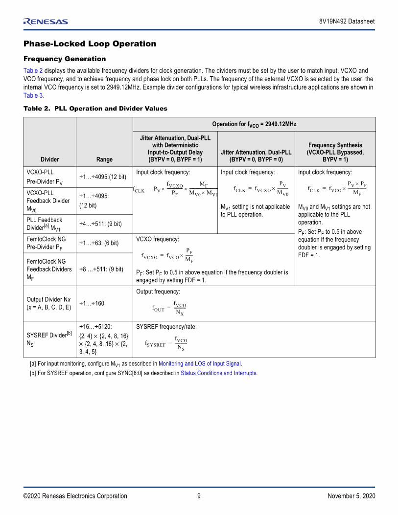
Frequency GenerationTable 2 displays the available frequency dividers for clock generation. The dividers must be set by the user to match input, VCXO and VCO frequency, and to achieve frequency and phase lock on both PLLs. The frequency of the external VCXO is selected by the user; the internal VCO frequency is set to 2949.12MHz. Example divider configurations for typical wireless infrastructure applications are shown in Table 3. Table 2. PLL Operation and Divider Values
Divider Range
Operation for fVCO = 2949.12MHz
Jitter Attenuation, Dual-PLL with Deterministic
Input-to-Output Delay(BYPV = 0, BYPF = 1)
Jitter Attenuation, Dual-PLL(BYPV = 0, BYPF = 0)
Frequency Synthesis(VCXO-PLL Bypassed,
BYPV = 1)
VCXO-PLLPre-Divider PV
÷1…÷4095:(12 bit)Input clock frequency: Input clock frequency:
MV1 setting is not applicable to PLL operation.
Input clock frequency:
MV0 and MV1 settings are not applicable to the PLL operation.PF: Set PF to 0.5 in above equation if the frequency doubler is engaged by setting FDF = 1.
VCXO-PLL Feedback Divider MV0
÷1…÷4095:(12 bit)
PLL Feedback Divider[a] MV1
[a] For input monitoring, configure MV1 as described in Monitoring and LOS of Input Signal.
÷4…÷511: (9 bit)
FemtoClock NGPre-Divider PF
÷1…÷63: (6 bit) VCXO frequency:
PF: Set PF to 0.5 in above equation if the frequency doubler is engaged by setting FDF = 1.
FemtoClock NGFeedback Dividers MF
÷8 …÷511: (9 bit)
Output Divider Nx(x = A, B, C, D, E) ÷1…÷160
Output frequency:
SYSREF Divider[b] NS
[b] For SYSREF operation, configure SYNC[6:0] as described in Status Conditions and Interrupts.
÷16…÷5120:2, 4 2, 4, 8, 16 2, 4, 8, 16 2, 3, 4, 5
SYSREF frequency/rate:
fCLK PVfVCXO
PF--------------------
MFMV0 MV1------------------------------------= fCLK fVCXO
PVMV0--------------= fCLK fVCO
PV PFMF
-----------------------=
fVCXO fVCOPFMF---------=
fOUTfVCONX
---------------=
fSYSREFfVCONS
---------------=

10©2020 Renesas Electronics Corporation November 5, 2020
8V19N492 Datasheet
VCXO-PLLThe prescaler PV and the VCXO-PLLs feedback divider MV0 and MV1 require configuration to match the input frequency to the VCXO-frequency. The BYPF setting allows to route the VCXO-PLLs feedback path through the MV0 divider. Alternatively, the feedback path is routed through the second PLL and both the MV0 and MV1 feedback divider. MV0 has a divider value range of 12 bit; MV1 has 9 bit.
The feedback path through the second PLL, in combination with the divider setting PF=÷1, is the preferred setting for achieving deterministic delay from the clock input to the outputs. Multiple divider settings are available to enable support for input frequencies of e.g. 245.76, 122.88, 61.44 and 30.72MHz and the VCXO-frequencies of 122.88MHz, 61.44, 38.4, 30.72 and 245.76 MHz. In addition, the range of available input and feedback dividers allows to adjust the phase detector frequency independent on the input and VCXO frequencies. In general, the phase detector may be set into the range from 120kHz to the input reference frequency. The VCXO-PLL charge pump current is controllable via a register and can be set in 50µA steps from 50µA to 1.6mA. The VCXO-PLL may be bypassed: the FemtoClockNG PLL locks to the pre-divider input frequency.
Table 3. Example Configurations for fVCXO = 122.88MHz[a]
[a] BYPF=0
Input Frequency(MHz)
VCXO-PLL Divider SettingsfPFD
(MHz)PV MV0
245.76
2 1 122.88
32 16 7.68
256 128 0.96
2048 1024 0.12
122.88
1 1 122.88
16 16 7.68
128 128 0.96
1024 1024 0.12
Table 4. Example Configurations for fVCXO = 38.4MHz[a]
[a] BYPF=0
Input Frequency(MHz)
VCXO- PLL Divider SettingsfPFD
(MHz)PV MV0
245.76
32 5 7.68
128 20 1.92
512 80 0.48
2048 320 0.12
122.88
16 5 7.68
64 20 1.92
256 80 0.48
1024 320 0.12

11©2020 Renesas Electronics Corporation November 5, 2020
8V19N492 Datasheet
FemtoClockNG PLLThis PLL locks to the output signal of the VCXO-PLL (BYPV=0). It requires configuration of the frequency doubler FDF or the pre-divider PF and the feedback divider MF to match the VCXO-PLL frequency to the VCO frequency of 2949.12MHz. This PLL is internally configured to high-bandwidth. Best phase noise is typically achieved by engaging the internal frequency doubler (FDF= 1, x2). If engaged, the signal from the first PLL stage is doubled in frequency, increasing the phase detector frequency of the FemtoClockNG PLL. Enabling the frequency doubler disables the frequency pre-divider PF. If the frequency doubler is not used (FDF=0), the PF pre-divider has to be configured. Typically PF is set to ÷1 to keep the phase detector frequency as high as possible. Set PF to other divider values to achieve specific frequency ratios (1 to 19.2, 1 to 76.8, etc.) between first and second PLL stage.
Table 5. VCXO-PLL Bypass Settings
BYPV Operation
0 VCXO-PLL operation.
1VCXO-PLL bypassed and disabled. The reference clock for the FemtoClockNG PLL is the input clock divided by the pre-divider PV. The input clock selection must be set to manual by the user. Clock switching and holdover are not defined. Device will not attenuate input jitter. No external VCXO component and loop filter required.
Table 6. PLL Feedback Path Settings
BYPF Operation[a]
0 VCXO-PLL feedback path through the MV0 divider. FemtoClockNG feedback path uses the MF divider.
1 VCXO-PLL feedback path through the MV1 MV0 dividers. FemtoClockNG feedback path uses the MF divider. Preferred setting for achieving deterministic delay from input to the outputs.
[a] Regardless of the selected internal feedback path, the MV1 divider should be set to match its internal output frequency to the input reference frequency: the MV1 output signal is the internal reference for input loss-of-signal detect.
Table 7. Frequency Doubler
FDF Operation
0 Frequency doubler off. PF divides clock signal from VCXO-PLL or input (in bypass)
1 Frequency doubler on (x2). Signal from VCXO-PLL or input (in bypass) is doubled in frequency. PF divider has no effect.

12©2020 Renesas Electronics Corporation November 5, 2020
8V19N492 Datasheet
Channel Frequency DividerThe device supports five independent channels A to E, each of them has an channel frequency divider Nx (x = A to E) that divides the VCO frequency to the output frequency. Each divider be individually set to a value in the range of ÷1 to ÷160. See Table 9 for typical divider values and Table 28 for the complete set of supported divider values
Table 8. Example PLL Configurations
VCXO-Frequency
(MHz)
FemtoClock NG Divider Settings Output Frequency
(MHz)FDF PF MF Nx[a]
122.88 x2 – 10
123468
1216
2949.121474.56983.04737.28491.52368.64245.76184.32
122.88 – 1 20
123468
1216
2949.121474.56983.04737.28491.52368.64245.76184.32
[a] x = A to E
Table 9. Integer Frequency Divider Settings
Channel Divider Nx[a]
Output Clock Frequency (MHz)
fVCO = 2949.12 (MHz)
÷1 2949.12
÷2 1474.56
÷3 983.04
÷4 737.28
÷6 491.52
÷8 368.64
÷12 245.76
÷16 184.32
÷24 122.88
÷30 98.304
÷32 92.16
÷36 81.92

13©2020 Renesas Electronics Corporation November 5, 2020
8V19N492 Datasheet
Redundant InputsThe two inputs are compatible with LVDS, LVPECL signal formats and also support single-ended signals (LVCMOS, see Section “Application Information” on page 67 for applicable input interface circuits).
Monitoring and LOS of Input SignalThe two inputs of the device are individually and permanently monitored for activity. Inactivity is defined by a static input signal.
he clock input monitors compare the device input frequency (fCLK) to the frequency of the VCO divided by MV1 (regardless of the internal feedback path using or not using MV1). A clock input is declared invalid with the corresponding LOS (Loss-of-input-signal) indicator bit set after three consecutive missing clock edges. For correct operation of the LOS detect circuit, MV1 must be powered-on by setting PD_MV1 = 0. The MV1 divider must be set so that the LOS detect reference frequency matches the input frequency. For instance, if the input frequency is 245.76MHz, MV1 should be set to ÷12: The VCO frequency of 2949.12MHz divided by 12 equals the input frequency of 245.76MHz. For an input frequency of 122.88MHz, set MV1 to ÷24. Failure to set MV1 to match the input frequency will result in added latency to the LOS circuit (if fVCO ÷ MV1 < fCLK) or false LOS indication (if fVCO ÷ MV1 > fCLK). The minimum frequency that the circuit can monitor is fVCO / MV1(MAX) = 5.77MHz. In applications with a lower input frequency than 5.77MHz, disable the monitor to trigger the status flags by setting BLOCK_LOR=1.
Input Re-ValidationA clock input is declared valid and the corresponding LOS bit is reset after the clock input signal returned for user-configurable number of consecutive input periods. This re-validation of the selected input clock is controlled by the CNTV setting (verification pulse counter).
÷48 61.44
÷60 49.152
÷64 46.08
÷72 40.96
÷96 30.72
÷120 24.576
÷128 23.04
[a] x = A to E
Table 9. Integer Frequency Divider Settings (Cont.)
Channel Divider Nx[a]
Output Clock Frequency (MHz)
fVCO = 2949.12 (MHz)

14©2020 Renesas Electronics Corporation November 5, 2020
8V19N492 Datasheet
Clock SelectionThe device supports multiple input selection modes: manual, short-term holdover and two automatic switch modes.
HoldoverIn holdover state, the output frequency and phase is derived from an internal, digital value based on previous frequency and phase information. Holdover characteristics are defined in Table 51.
Input PrioritiesConfigurable settings encompass four selectable priorities with the range 0 (lowest priority) to 3 (highest priority). A user may change the input priorities at any time. In the automatic switch modes, input priority changes may cause immediate input selection changes.
Table 10. Clock Selection Settings
Mode Description Application
Manual
nM/A=00
Input selection follows user-configuration of SEL[1:0]. Selection is never changed by the internal state machine. A failing reference clock will cause a LOS event and the PLL will unlock if the failing clock is selected. Re-validation of the selected input clock will result in the PLL to re-lock on that input clock.
Startup and external selection control
Automatic
nM/A=01
Input selection follows LOS status by user preset input switch priorities. A failing input clock will cause a LOS event for that clock input. If the selected clock has a LOS event, the device will immediately initiate a clock failover switch. The switch target is determined by pre-set input priorities.No valid clock scenario:If no valid input clocks exist, the device will not attempt to switch and will not enter the holdover state. The PLL is not locked. Re-validation of any input clock that is not the selected clock will result in the PLL to attempt to lock on that input clock.See “Revertive Switching”
Multiple inputs with qualified clock signals
Short-term Holdover
nM/A=10
Input selection follows user-configuration of SEL[1:0]. Selection is never changed by the internal state machine. A failing reference clock will cause a LOS event. If the selected reference fails, the device will enter holdover immediately. Re-validation of the selected input clock is controlled by the CNTV setting. A successful re-validation will result in the PLL to re-lock on that input clock.See “Short-Term Holdover”
Single reference
Automatic with holdover
nM/A=11
Input selection follows LOS status by user preset input priorities. Each failing input clock will cause a LOS event for that clock input. If the selected clock detects a LOS event, the device will go into holdover and the hold-off down-counter (CNTH) starts. The device initiates a clock failover switch after expiration of the hold-off counter. The switch target is determined by the preset input priorities.No valid clock scenario:If no valid input clocks exist, the device will not attempt to switch and will remain in the holdover state. Re-validation of any input clock will result in the PLL to attempt to lock on that input clock.See “Automatic with Holdover (nM/A[1:0] = 11)” and See “Revertive Switching”
Multiple inputs
15©2020 Renesas Electronics Corporation November 5, 2020
8V19N492 Datasheet
Hold-off CounterA configurable down-counter applicable to the “Automatic with holdover” selection mode. The purpose of this counter is a deferred, user-configurable, input switch after a LOS event. The counter expires when a zero-transition occurs; this triggers a new reference clock selection. The counter is clocked by the frequency-divided VCXO-PLL signal. The CNTR setting determines the hold-off counter frequency divider and the CNTH setting the start value of the hold-off counter. For instance, set CNTR to a value of ÷131072 to achieve 937.5 Hz (or a period of 1.066 ms at fVCXO=122.88MHz): the 8-bit CNTH counter is clocked by 937.5Hz and the user-configurable hold-off period range is 0ms (CNTR=0x00) to 272ms (CNTR=0xFF). After the counter expires, it reloads automatically from the CNTH SPI register. After the LOS status bit (LS_CLK_n) for the corresponding input CLK_n has been cleared by the user, the input is enabled for generating a new LOS event.
The CNTR counter is only clocked if the device is configured in the clock selection mode “Automatic with holdover” AND the selected reference clock experiences a LOS event. Otherwise, the counter is automatically disabled (not clocked).
Revertive SwitchingRevertive switching: is only applicable to the two automatic switch modes shown in Table 10. Revertive switching enabled: Re-validation of any non-selected input clock(s) will cause a new input selection according to the user-preset input priorities (revertive switch). An input switch is only done if the re-validated input has a higher priority than the currently selected reference clock.
Revertive switching disabled: Re-validation of a non-selected input clock has no impact on the clock selection. Default setting is revertive switching disabled.
Short-Term HoldoverIf an LOS event is detected on the reference clock designated by the SEL[1:0] bits: Holdover begins immediately ST_REF, LS_REF go low immediately No transitions will occur of the active REF clock; ST_SEL[1:0] does not change The hold-off countdown is not active
When the designated reference clock resumes and has met the programmed validation count of consecutive rising edges: Holdover turns off ST_SEL[1:0] does not change ST_REF returns to 1
LS_REF can be cleared by an SPI write of 1 to that register
Automatic with Holdover (nM/A[1:0] = 11)If a LOS event is detected on the active reference clock: Holdover begins immediately Corresponding ST_REF and LS_REF go low immediately Hold-off countdown begins immediately.
During this time, all clocks continue to be monitored and their respective ST_CLK, LS_CLK flags are active. LOS events will be indicated on ST_CLK, LS_CLK when they occur.
If the active reference clock (or any CLK) resumes and is validated during the hold-off countdown: Its ST_CLK status flag will return high and the LS_CLK is available to be cleared by an SPI write of 1 to that register bit. No transitions will occur of the active REF clock; ST_SEL[1:0] does not change and the ST_REF, LS_REF remain low even if active
REF clock has been validated and its ST_CLK status bit returns high Revertive bit has no effect during this time (whether 0 or 1)

16©2020 Renesas Electronics Corporation November 5, 2020
8V19N492 Datasheet
When the hold-off countdown reaches zero: If the active reference has resumed and has been validated during the countdown, it will maintain being the active reference clock
• ST_SEL1:0 does not change• ST_REF returns to 1• LS_REF can be cleared by an SPI write of 1 to that register• Holdover turns off and the VCXO-PLL attempts to lock to the active reference clock
If the active reference has not resumed, but another (sorted by next priority) clock input CLK_n is validated, then• ST_SEL1:0 changes to the new active reference• ST_REF returns to 1• LS_REF can be cleared by an SPI write of 1 to that register • Holdover turns off
If there is no validated CLK:• ST_SEL1:0 does not change• ST_REF remains low• LS_REF cannot be cleared by an SPI write of 1 to that register• Holdover remains active
Revertive capability returns if REVS = 1.
VCXO-PLL Lock DetectThe VCXO-PLL lock detect circuit uses the signal phase difference at the phase detector as loss-of-lock criteria. Loss-of-lock is reported if the actual phase difference is larger than a configurable phase detector window set by the MV0[2:0] and PV[2:0] configuration bits. A loss-of-lock state is reported through the nST_LOLV and nLS_LOLV status bit, see Table 22.
Loss-of-Lock Window Description
The selected clock input signal is the reference signal (CLK) for lock detection. The rising edge of CLK defines the reference point t0. PV configures the start of the lock window tB (which occurs before t0) and MV0 configures the end of the window tE (which occurs after t0). The width of the lock window is defined by tE - tB. The VCXO-PLL declares lock when the rising edge of the feedback signal (FB) is within this window, otherwise the PLL reports loss-of-lock.
Figure 3. Lock Detect Window
CLK
FB
t0tB tE
PFDCP
÷MV0
LFV
÷PV
BYPF
÷MV1
0
1
CLK
FB
InputVCXO
VCXO
VCOLock detected if FB in this window

17©2020 Renesas Electronics Corporation November 5, 2020
8V19N492 Datasheet
Figure 3 shows that PV configures the start and MV0 the end of the window in integer multiples of PLL input and feedback periods. Both PV and MV0 use 3 configuration bits with valid settings from 010 to 111 (2 to 7, decimal). This range allows configuring both tS and tE from 3 to 127 periods of the input signal (TIN) and the feedback signal (TFB), respectively, is implied.
Loss-of-Lock Window Configuration Example
With given PV, MV0 and MV1 divider values, select the corresponding PV and MV0 settings from Table 12 and apply the PV and MV0 values to the PV[1:0] and MV0[1:0] registers. Table 11 shows the lock window calculation formulas. For instance, if an input frequency of 245.76MHz and a PV divider of 128 is desired, set PV[1:0] to a binary value of 100 (decimal 4). This results in tB = -61.035ns (15 periods of 4.069ns). With a VCXO-PLL (BYPF=0) and a VCXO frequency of 122.88MHz and MV0=64, select 011 (decimal 3) resulting in tE = 56.96ns (7 periods of 8.138 ns) and an overall lock detect window of tE - tB = 56.96ns + 61.035ns = 118.001ns. The user may select a smaller lock detect window. For instance, a PV divider of 128 allows to set PV[1:0] to 010, 011 or 100 (decimal 2 to 4). Correspondingly, a MV0 divider of 64 allows MV0[1:0] settings from 010 to 011 (decimal 2 to 3). With smaller settings, the lock detect window size is reduced exponentially.
PV[1:0]=000 will set tB to 0.5*TREF and PV[1:0]=001 will set tB to 1.5*TREF.
MV0[1:0]=000 will set tE to 0.5*TREF and MV0[1:0]=001 will set tE to 1.5*TREF.
FemtoClockNG Loss-of-Lock (LOLF)FemtoClockNG-PLL loss of lock is signaled through the nST_LOLF (momentary) and nLS_LOLF (sticky, resettable) status bits and can reported as hardware signal on the LOCK output as well as an interrupt signal on the nINT output.
Table 11. tB and tE Calculation
Operation
Jitter Attenuation, Dual-PLL with deterministic Input-to-Output Delay
(BYPV = 0, BYPF = 1)
Jitter Attenuation, Dual-PLL
(BYPV = 0, BYPF = 0)
tB
tE
Table 12. Recommended Lock Detector Phase Window Settings
PV Divider Value PV[1:0] Setting MV0 Divider Value MV0[1:0] Setting
1 - 31 N/A 1 - 31 N/A
32 - 63 010 32 - 63 010
64-127 ≤011 64-127 ≤011
128-255 ≤100 128-255 ≤100
256-511 ≤101 256-511 ≤101
512-1023 ≤110 512-1023 ≤110
1024 and higher ≤111 1024 and higher ≤111
tB2PV 1–
fCLK--------------------------–=
tE2MV0 1– MV1
fVCO--------------------------------------------------------= tE
2MV0 1–fVCXO
-------------------------------=

18©2020 Renesas Electronics Corporation November 5, 2020
8V19N492 Datasheet
Channel, Output, and JESD204B Logic
ChannelEach of the four channels A to D consists of one to two clock and associated one to three SYSREF outputs. Each SYSREF output in a channel can be individually configured to generate JESD204B (SYSREF) signals or copy the clock signal of that channel. The fifth channel (E) consists of two clock outputs without SYSREF support in that channel.
If JESD204B/SYSREF operation is assigned to a QREF output, the channel logic controls the outputs: outputs automatically turn on and off in a SYSREF sequence. QREF outputs configured to clock operation can individually configure output states.
Differential Outputs
Table 13. Channel Configuration[a]
[a] x = A to E. y = A0, A1, B0, B1, C, D, E0, E1; r = A0, A1, A2, B0, B1, C, D
MUX 0 1
Description Clock configuration JESD204B
QCLK_yClock signal
Clock signal
QREF_r SYSREF/JESD204B
Frequency Divider QCLK_y and QREF_r: NxQCLK_y: NxQREF_r: NS (Global to all QREF_r)
Phase DelayQCLK_y and QREF_r: CLK_xREF_r settings do not apply
QCLK_y: CLK_xQREF_r: REF_r
Power Down Per output Per channel
Output Enable Per output Per output
Table 14. Output Features
Output Style Amplitude[a]
[a] Amplitudes are measured single-endedly. Differential amplitudes supported are 500, 1000, 1500 and 2000mV
Disable Power Down Termination
QCLK_y, QREF_r(Clock)
LVPECL 250–1000 mV4 steps
Yes Yes50 to VT
LVDS 100 differential[b]
[b] AC coupling and DC coupling supported.
QREF_r(SYSREF)
LVDS250–1000 mV
4 stepsControlled by SYSREF[c]
[c] State of SYSREF outputs is controlled by an internal SYSREF state machine.
100 differentialb
QOSCLVPECL 250–750 mV
3 stepsYes Yes
50 to VT
LVDS 100 differentialb

19©2020 Renesas Electronics Corporation November 5, 2020
8V19N492 Datasheet
Table 15. Individual Clock Output Settings[a]
PD[b]STYL
E EN[c] A[1:0][d]Output Power Termination State
Amplitude (mV)
1 X X X Off 100 differential or no termination Off X
0
0
0 XX
On
100 differential (LVDS)
Disable (logic low) X
1
00
Enable
250
01 500
10 750
11 1000
1
0 XX 50 to VT (LVPECL)
Enable
X
1
00 50 to VT = VDD_V - 1.50V (LVPECL) 250
01 50 to VT = VDD_V - 1.75V (LVPECL) 500
10 50 to VT = VDD_V - 2.00V (LVPECL) 750
11 50 to VT = VDD_V - 2.25V (LVPECL) Enable 1000
[a] Applicable to clock outputs: QCLK_y and QREF_r outputs in clock mode (MUX_r = 0)[b] Power-down modes are available for the individual channels A-E and the outputs QCLK_y (A0 to E1).[c] Output enable is supported on each individual QCLK_y and QREF_r output.[d] Output amplitude control is supported on each individual QCLK_y and QREF_r output.
Table 16. Individual SYSREF Output Settings[a]
[a] Applicable QREF_r outputs when configured as SYSREF output (MUX_r = 1).
PD STYLE EN nBIAS A[1:0]Output Power Termination State
Amplitude (mV)
1 X X X X Off 100 differential or no termination Off X
0
0
0
0
X
On[b]
[b] Output amplitude should be set to a 500 mV swing (A[1:0] to 01) by SPI. SYSREF output states are controlled by an internal state machine. An internal SYSREF event will automatically turn SYSREF outputs on. After the event, outputs are automatically turned off. Setting nBIAS = 1 will bias powered-off outputs to the LVDS midpoint voltage.
100 differential (LVDS)
Disable (logic low) X
1
00011011
Enable
250500750
1000
X 1 XX Line bias[c]
[c] Output (both Q, and nQ) bias the line to the differential signal cross-point voltage. Available if output is AC-coupled and set to LVDS style
XX
1
0
0
X
50 to VT = VDD_V - 1.50V (LVPECL)
Disable (logic low) X
1
00011011
Enable
250500750
1000
20©2020 Renesas Electronics Corporation November 5, 2020
8V19N492 Datasheet
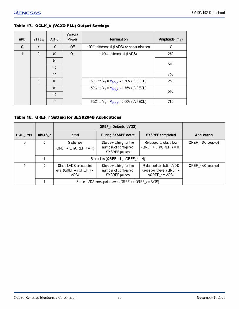
Table 17. QCLK_V (VCXO-PLL) Output Settings
nPD STYLE A[1:0]Output Power Termination Amplitude (mV)
0 X X Off 100 differential (LVDS) or no termination X
1 0 00 On 100 differential (LVDS) 250
01500
10
11 750
1 00 50 to VT = VDD_V - 1.50V (LVPECL) 250
01 50 to VT = VDD_V - 1.75V (LVPECL)500
10
11 50 to VT = VDD_V - 2.00V (LVPECL) 750
Table 18. QREF_r Setting for JESD204B Applications
BIAS_TYPE nBIAS_r
QREF_r Outputs (LVDS)
ApplicationInitial During SYSREF event SYSREF completed
0 0 Static low(QREF = L, nQREF_r = H)
Start switching for the number of configured
SYSREF pulses
Released to static low (QREF = L, nQREF_r = H)
QREF_r DC coupled
1 Static low (QREF = L, nQREF_r = H)
1 0 Static LVDS crosspoint level (QREF = nQREF_r =
VOS)
Start switching for the number of configured
SYSREF pulses
Released to static LVDS crosspoint level (QREF =
nQREF_r = VOS)
QREF_r AC coupled
1 Static LVDS crosspoint level (QREF = nQREF_r = VOS)

21©2020 Renesas Electronics Corporation November 5, 2020
8V19N492 Datasheet
Output Phase DelayOutput phase delay is independently supported on both clock and SYSREF outputs.
The phase delay on clock outputs ΦCLK_x, SYSREF outputs coarse delay ΦREF_r and global delay ΦREF_S is derived from the internal VCO frequency of the second PLL (FemtoClock NG PLL). In configurations bypassing the second PLL by setting SRC = 1, the delay unit is derived from the frequency of the external VCXO: use fVCXO instead of fVCO in Table 19.
Configuration for JESD204B Operation
Synchronizing SYSREF and Clock Output DividersThe SYNC[6:0] divider controls the release of SYSREF pulses at coincident QCLK_y clock edges. For SYSREF operation, set the SYNC divider value to the least common multiple of the clock divider values Nx (x = A to E). For instance, if NA = NB = ÷2, NC = ND = ÷3, NE = ÷4, set the SYNC divider to ÷12.
SYSREF GenerationA SYSREF event is the generation of one or more consecutive pulses on the QREF outputs. An event can be triggered by SPI commands or by a signal-transition on the EXT_SYS input. The number of SYSREF pulses generated is programmable from 1 to 255. The SYSREF signal can also be programmed to be continuous. The SYSREF pulse rate is configurable to the frequencies shown in Table 20. SYSREF output pulses are aligned to coincident rising clock edges of the clock outputs QCLK_y. Device settings for phase alignment between QCLK_y and QREF_r outputs is detailed in the section, QCLK to QREF Phase Alignment. The following SYSREF pulse generation modes are available and configurable by SPI: Counted pulse mode – 1 to 255 pulses are generated by the device. SYSREF activity stops automatically after the transmission of the
selected number of pulses and the QREF output powers down. Continuous mode – The SYSREF signal is a clock signal.
Table 19. Delay Circuit Settings
Delay Circuit Unit Steps Range (ns) Alignment[a]
[a] Default configuration (all delay settings = 0). REF_r coarse delay values are exact, fine delay value vary over PVT by ±20%.
Clock[b] CLK_x
[b] Clock output inversion supported by setting phase delay to 180° setting.
256 0–86.466[c]
[c] Exact delay value.
Incident rising clock edges are aligned, independent on the divider
N_x across channels
SYSREF REF_r
Coarse delay:8 0–1.187[c]
SYSREF rising edge is aligned to the incident rising clock edge across
channelsFine delay:0, 25, 50, 75, 85, 110, 135, 160 ps
8 0–0.160[d]
[d] ±20% delay variation over PVT.
SYSREF (Global)REF_S
256 0–86.466[c] Global alignment of SYSREF signals
1fVCO--------------- 339ps=
12fVCO------------------- 169ps=
1fVCO--------------- 339ps=
22©2020 Renesas Electronics Corporation November 5, 2020
8V19N492 Datasheet
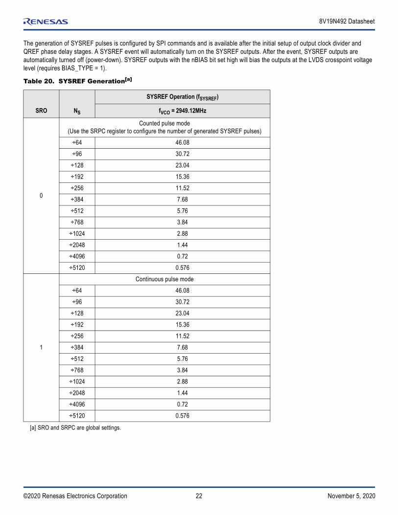
The generation of SYSREF pulses is configured by SPI commands and is available after the initial setup of output clock divider and QREF phase delay stages. A SYSREF event will automatically turn on the SYSREF outputs. After the event, SYSREF outputs are automatically turned off (power-down). SYSREF outputs with the nBIAS bit set high will bias the outputs at the LVDS crosspoint voltage level (requires BIAS_TYPE = 1).
Table 20. SYSREF Generation[a]
[a] SRO and SRPC are global settings.
SRO NS
SYSREF Operation (fSYSREF)
fVCO = 2949.12MHz
0
Counted pulse mode(Use the SRPC register to configure the number of generated SYSREF pulses)
÷64 46.08
÷96 30.72
÷128 23.04
÷192 15.36
÷256 11.52
÷384 7.68
÷512 5.76
÷768 3.84
÷1024 2.88
÷2048 1.44
÷4096 0.72
÷5120 0.576
1
Continuous pulse mode
÷64 46.08
÷96 30.72
÷128 23.04
÷192 15.36
÷256 11.52
÷384 7.68
÷512 5.76
÷768 3.84
÷1024 2.88
÷2048 1.44
÷4096 0.72
÷5120 0.576
23©2020 Renesas Electronics Corporation November 5, 2020
8V19N492 Datasheet
Internal SYSREF GenerationSYSREF generation is set to internal (SRG = 0). The SRO setting defines if SYSREF pulses are counted or continuous and the NS[6:0] divider sets the frequency. In counted pulse mode, the SRPC register contains the number of pulses to generate. Any number from 1 to 255 pulses may be generated. SYSREF pulses are generated upon completion of the SPI command RS (SYSREF release). Setting RS activates the SYSREF outputs, loads the number of pulses from the SRPC register and starts the generation of SYSREF pulses synchronized to the incident edge of the clock signals. After the programmed number of pulses are generated, SYSREF outputs will go into logic low state or bias the output voltage to the static LVDS crosspoint level (see Table 21 for settings and details). In continuous mode, SYSREF is a clock signal and the content of the SRPC signal is ignored.
External SYSREF GenerationSYSREF generation is set to external (SRG = 1): SYSREF pulses are generated in response to the detection of a rising edge at the EXT_SYS input. The EXT_SYS input rising edge releases SYSREF pulses. Both SRO and SRPC register settings apply as in internal SYSREF generation mode for generating single shot and repetitive SYSREF output signals. Set RS = 1 to prepare for SYSREF generation; the generation of SYSRE pulses is triggered by a rising edge at EXT_SYS pin.
QCLK to QREF (SYSREF) Phase AlignmentFigure 4 and Table 21 show how to achieve output phase alignment between the QCLK_y clock and the QREF_r SYSREF outputs in internal SYSREF generation mode (SRG=0). The closest (smallest phase error) output alignment is achieved by setting the clock phase delay register QCLK_Y to 0x00 (clock), the SYSREF output phase delay register REF_r to 0x01 and the global REF_S delay register to 0x29. With a SYSREF phase delay setting of 0x01 or less, REF_r = 0, the QREF_r output phase is in advance of the QCLK_y phase, which is applicable in JESD204B application. Phase delay settings and propagation delays are independent on the clock and SYSREF frequencies, but independent of the SYSREF generation mode (SRG = 0 or SRG = 1). Recommended phase delay setting several device configurations are shown in Table 21.

24©2020 Renesas Electronics Corporation November 5, 2020
8V19N492 Datasheet
Figure 4. QCLK to QREF Phase Alignment
Deterministic Phase Relationship and Phase AlignmentInput to output delay is deterministic when the device is configured as dual PLL with the BYPV = 0, BYPF = 1 (PLL feedback path through MV0 MV1). Refer to the application note AN-952: 8V19N480/490 Design Guide for JESD204B Output Phase Alignment and Termination for additional information on phase alignment, termination and coupling techniques.
Table 21. Recommended Delay Settings for Closest Clock-SYSREF Output Phase Alignment[a]
[a] QCLK and QREF outputs are aligned on the incident edge.
Divider Configuration CLK_y REF_r REF_S
NA-E=÷3NS=÷384
0x00 0x01 0x29
NA-E = ÷3, ÷6,÷12NS=÷384
0x00 0x01 0x29
NA-E = ÷8NS=÷384
0x00 0x03 0x00
QCLK_yQCLK_y = 0x00
QCLK_yQCLK_y = 0x00
QREF_rREF_r = 0x01REF_r_F = 1
QCLK_yQCLK_y = 0x00
QCLK_yQCLK_y = 0x00
QREF_rREF_r = 0x00REF_r_F = 1
QREF_rREF_r = 0x00REF_r_F = 1
Output Phase Alignment
QREF_r in advance of QCLK_y
= 169ps
= 338ps
25©2020 Renesas Electronics Corporation November 5, 2020
8V19N492 Datasheet
Status Conditions and InterruptsThe device has an interrupt output to signal changes in status conditions. Settings for status conditions may be accessed in the Status registers. The devices has several conditions that can indicate faults and status changes in the operation of the device. These are shown in Table 22 and can be monitored directly in the status registers. Status bits (named: ST_condition) are read-only and reflect the momentary device status at the time of read-access. Several status bits are also copied into latched bit positions (named: LS_condition). The latched version is controlled by the corresponding fault and status conditions and remains set (“sticky”) until reset by the user by writing “1” to the status register bit. The reset of the status condition has only an effect if the corresponding fault condition is removed, otherwise, the status bit will set again.
Setting a status bit on several latched registers can be programmed to generate an interrupt signal (nINT) via settings in the Interrupt Enable bits (named: IE_condition). A setting of “0” in any of these bits will mask the corresponding latched status bit from affecting the interrupt status pin. Setting all IE bits to 0 has the effect of disabling interrupts from the device. Interrupts are cleared by resetting the appropriate bit(s) in the latched register after the underlying fault condition has been resolved. When all valid interrupt sources have been cleared in this manner, this will release the nINT output until the next unmasked fault
Table 22. Status Bit Functions
Status Bit Function
Interrupt Enable BitMomentary Latched Description
Status if Bit is:
1 0
ST_CLK_0 LS_CLK_0 CLK 0 input status Active LOS IE_CLK_0
ST_CLK_1 LS_CLK_1 CLK 1 input status Active LOS IE_CLK_1
nST_LOLV nLS_LOLV VCXO-PLL loss of lock Locked Loss of lock IE_LOLV
nST_LOLF[a]
[a] nST_LOLV and nLS_LOLV report 1 (PLL locked) if the VCXO-PLL is bypassed by setting BYPV = 1
nLS_LOLF FemtoClockNG-PLL loss of lock Locked Loss of lock IE_LOLF
nST_HOLD nLS_HOLD Holdover Not in holdover Device in holdover IE_HOLD
ST_VCOF — FemtoClockNG VCO calibration Not completed Completed —
ST_SEL[1:0] — Clock input selection in auto-selection mode
00 = CLK_001 = CLK_1
10, 11 - not defined—
ST_REF LS_REF PLL reference status Valid reference[b]
[b] Manual and short-term holdover mode: 0 indicates if the reference selected by SEL[1:0] is lost, 1 if not lostAutomatic with holdover mode: 0 indicates the reference is lost and while still in holdover
Reference lost IE_REF
Table 23. LOCK Function
Status Bit (PLL)
Status reported on LOCK output
nLS_LOLV(VCXO-PLL)
nLS_LOLF(FemtoClockNG)
Locked[a]
[a] nST_LOLV and nLS_LOLV report 1 (PLL locked) if the VCXO-PLL is bypassed by setting BYPV = 1
Locked 1
Not locked 0
Not lockedLocked 0
Not locked 0

26©2020 Renesas Electronics Corporation November 5, 2020
8V19N492 Datasheet
Device Startup, Reset, and SynchronizationAt startup, an internal POR (power-on reset) resets the device and sets all register bits to its default value. The device forces the VCXO control voltage at the LFV pin to half of the power supply voltage to center the VCXO-frequency. In the default configuration the QCLK_y and QREF_r outputs are disabled at startup.
Recommended Configuration Sequence (In Order):1. (Optional) Set the value of the CPOL register bit to define the SPI read mode, so that SPI settings can be validated by subsequent SPI
read accesses. 2. Configure all PLL settings, output divider and delay circuits as well as other device configurations:
BYPF and BYPV for the desired PLL operation mode and configure the PLL dividers PV, MV0, MV1, MF and PF as required to achieve PLL lock. See Table 2 for details
VCXO-PLL lock detect window by configuring the phase settings MV0 and PV Charge pump currents for both PLLs (CPV[4:0] and CPF[4:0]) and POLV for the desired VCXO polarity (optional) OSVEN and OFFSET[4:0] for the VCXO-PLL static phase offset Channel dividers (see Table 8) MUX_r for the desired operation of the QREF_r outputs QCLK_y, QREF_r and QOSC output features such as desired output power-down state, style and amplitude Desired input selection and monitoring modes: this involves nM/A[1:0] and SEL[1:0] for input selection. In any of the automatic
modes, configure PRIO[1:0]_n, and REVS. Configure the CNTH[7:0], CNTR[1:0] counters for the desired holdover characteristics and DIV4_VAL, CNTV[1:0] for input revalidation if applicable to the operation mode.
Individual CLK_X and REF_r registers and the global delay REF_S register for the desired phase delay between clock and SYSREF outputs; see (link to phase alignment section).
Interrupt enable configuration bits IE_status_condition, as desired for fault reporting on the nINT output3. For SYSREF operation:
Configure the NS and SYNC divider as described in the section Status Conditions and Interrupts Configure the SYSREF registers SRG, SRO and SRPC[7:0] according to the desired SYSREF operation
4. Set the initialization bit INIT_CLK. This will initiate all divider and delay circuits and synchronize them to each other. The INIT_CLK bit will self-clear.
5. Set both the RELOCK bit and PB_CAL bit. This step should not be combined with the previous step (setting INIT_CLK) in a multi SPI-byte register access. Both bits will self-clear.
6. Clear the FVCV bit to release the VCXO control voltage and VCXO-PLL will attempt to lock to the input clock signal starting from its center frequency.
7. Clear the status flags. 8. At this point, the basic configuration of the registers 0x00 to 0x73 should be completed and the SPI transfer ended (set nCS to high
level). 9. In a separate SPI write access, enable the outputs as desired by accessing the output-enable registers 0x74 and 0x76.10. For SYSREF operation: set the RS bit to start (or re-start) generating the configured number of SYSREF pulses. The RS bit will auto-clear.
• In internal SYSREF generation mode (SRG = 0) the SYSREF pulses are generated as a result of setting the RS bit.• In external SYSREF mode the SYSREF pulses are generated at the next rising edge of the EXT_SYS input.
Reserved registers and registers in the address range 0x78 to 0xFF should not be used. Do not write into any registers in the 0x78 to 0xFF range.

27©2020 Renesas Electronics Corporation November 5, 2020
8V19N492 Datasheet
Changing Frequency Dividers and Phase Delay Values
Clock Frequency Divider and Delay
The following procedure must be applied for a change of a clock divider and phase delay value NA-E, and CLKA-E:1. (Optional) Set the value of the CPOL register to define the SPI read mode, so that SPI settings can be validated by subsequent SPI
read accesses. 2. (Optional) Disable the outputs whose frequency divider or delay value is changed. 3. Configure the NA-E dividers and the delay circuits CLKA-E to the desired new values. 4. (Optional) configure the SYNC divider if required for synchronization between clock and SYSREF signals. 5. Set the initialization bit INIT_CLK. This will initiate all divider and delay circuits and synchronize them to each other. The INIT_CLK bit
will self-clear. During this initialization step, all QCLK_y and QREF_r outputs are reset to the logic low state. 6. Set the RELOCK bit. This step should not be combined with the setting INIT_CLK in a multi SPI-byte register access. Bit will self-clear. 7. (Optional) enable the outputs whose frequency divider was changed.
SYSREF Frequency Divider, Delay and Starting/Re-Starting SYSREF Pulse Sequences
The following procedure must be applied for a change of a SYSREF divider and phase delay value NS and REF_S:1. (Optional) Set the value of the CPOL register to define the SPI read mode, so that SPI settings can be validated by subsequent SPI
read accesses. 2. (Optional) Disable the outputs whose frequency divider or delay value is changed. 3. Configure any NS divider and any delay circuits REF_S to their desired new values. 4. Configure the SYNC divider if required for synchronization between clock and SYSREF signals. 5. Set the initialization bit INIT_CLK. This will initiate all divider and delay circuits and synchronize them to each other. The INIT_CLK bit
will self-clear. During this initialization step, all QCLK_y and QREF_r outputs are reset to the logic low state.6. Set the RELOCK bit. This step should not be combined with the setting INIT_CLK in a multi SPI-byte register access. Bit will self-clear.7. Set the SRO bit to counted pulse mode or to continues pulse mode, as desired8. (Optional) enable the outputs whose frequency divider was changed.9. For SYSREF operation: set the RS bit to start (or re-start) generating the configured number of SYSREF pulses. The RS bit will auto-clear.
In internal SYSREF generation mode (SRG = 0) the SYSREF pulses are generated as a result of setting the RS bit. In external SYSREF mode the SYSREF pulses are generated at the next rising edge of the EXT_SYS input.
SPI InterfaceThe device has a 3-wire serial control port capable of responding as a slave in an SPI configuration to allow read and write access to any of the internal registers for device programming or read back. The SPI interface consists of the SCLK (clock), SDAT (serial data input and output), and nCS (chip select) pins. A data transfer consists any integer multiple of 8 bits and is always initiated by the SPI master on the bus. Internal register data is organized in SPI bytes of 8 bit each.
If nCS is at logic high, the SDAT data I/O is in high-impedance state and the SPI interface of the device is disabled.
In a write operation, data on SDAT will be clocked in on the rising edge of SCLK. In a read operation, data on SDAT will be clocked out on the falling or rising edge of SCLK depending on the CPOL setting (CPOL=0: output data changes on the falling edge, CPOL=1: output data changes on the rising edge).
Starting a data transfer requires nCS to set and hold at logic low level during the entire transfer. Setting nCS = 0 will enable the SPI interface with SDAT in data input mode. The master must initiate the first 8-bit transfer. The first bit presented by the SPI master in each transfer is the LSB (least significant bit). The first bit presented to the slave is the direction bit R/nW (1 = Read, 0 = Write) and the following seven bits are the address bits A[0:6] pointing to an internal register in the address space 0 to 127.

28©2020 Renesas Electronics Corporation November 5, 2020
8V19N492 Datasheet
Read operation from an internal register: a read operation starts with an 8 bit transfer from the master to the slave: SDAT is clocked on the rising edge of SCLK. The first bit is the direction bit R/nW which must be to 1 to indicate a read transfer, followed by 7 address bits A[0:6]. After the first 8 bits are clocked into SDAT, the SDAT I/O changes to output: The register content addressed by A[0:6] are loaded into the shift register and the next 8 SCLK falling (CPOL=1) clock cycles will then present the loaded register data on the SDAT output and transfer these to the master. Transfers must be completed with de-asserting nCS after any multiple 8 SCLK cycles. If nCS is de-asserted at any other number of SCLKs, the SPI behavior is undefined. SPI byte (8 bit) and back-to-back read transfers of multiple registers are supported with an address auto-increment. During multiple transfers, nCS must stay at logic low level and SDAT will present multiple registers (A), (A+1), (A+2), etc. with each 8 SCLK cycles. During SPI Read operations, the user may continue to hold nCS low and provide further bytes of data for up to a total of 127 bytes in a single block read.
Write operation to a device register: During a write transfer, a SPI master transfers one or more bytes of data into the internal registers of the device. A write transfer starts by asserting nCS to low logic level. The first bit presented by the master must set the direction bit R/nW to 0 (Write) and the 7 address bits A[0:6] must contain the 7-bit register address. Bits D0 to D7 contain 8 bit of payload data, which is written into the register addressed by A[0:6] at the end of a 8-bit write transfer. Multiple, subsequent register transfers from the master to the slave are supported by holding nCS asserted at logic low level during write transfers. The 7 bit register address will auto-increment. Transfers must be completed with de-asserting nCS after any multiple 8 SCLK cycles. If nCS is de-asserted at any other number of SCLKs, the SPI behavior is undefined.
End of transfer: After nCS is de-asserted to logic 1, the SPI bus is available to transfers to other slaves on the SPI bus. See also the READ diagram (Figure 5) and WRITE (Figure 6) displaying the transfer of two bytes of data from and into registers.
Registers 0x78 to 0xFF. Registers in the address range 0x78 to 0xFF should not be used. Do not write into any registers in the 0x78 to 0xFF range.
Figure 5. Logic Diagram: READ Data from Registers for CPOL = 0 and CPOL = 1
Figure 6. Logic Diagram: WRITE Data into Registers
D01 A0 A1 A2 A3 A4 A5 A6 D1 D2 D3 D4 D5 D6 D7 D0 D1 D2 D3 D4 D5 D6 D7
1 2 3 4 5 6 7 8 9 10 11 12 13 14 15 16 17 18 19 20 21 22 23
SCLK
nCS
SDAT, CPOL=0
SDAT, CPOL=1
Hi-Imp
0
Input R=1, 7-bit AddressOutput Register Data
(Address)Output Register Data
(Address+1)
Hi-Imp
1Hi-Imp A0 A1 A2 A3 A4 A5 A6 D0 D1 D2 D3 D4 D5 D6 D7 D0 D1 D2 D3 D4 D5 D6 D7 Hi-Imp
1 2 3 4 5 6 7 8 9 10 11 12 13 14 15 16 17 18 19 20 21 22 23
SCLK
nCS
SDAT 0Hi-Imp A0 A1 A2 A3 A4 A5 A6 D0
0
D1 D2 D3 D4 D5 D6 D7
Input nW=0, 7-bit Address Input Register Data (Address)Input Register Data
(Address+1)
D0 D1 D2 D3 D4 D5 D6 D7 Hi-Imp

29©2020 Renesas Electronics Corporation November 5, 2020
8V19N492 Datasheet
Figure 7. SPI Timing Diagram
Table 24. SPI Read / Write Cycle Timing Parameters
Symbol Parameter Test Condition Minimum Maximum Unit
fSCLK SCLK frequency 20 MHz
tS1 Setup time, nCS (falling) to SCLK (rising) 5 ns
tS2 Setup time, SDAT (input) to SCLK (rising) 5 ns
tS3 Setup time, nCS (rising) to SCLK (rising) 5 ns
tH1 Hold time, SCLK (rising) to SDAT (input) 5 ns
tH2 Hold time, SCLK (falling) to nCS (rising) 5 ns
tPD2F Propagation delay, SCLK (falling) to SDAT CPOL = 0 12 ns
tPD2R Propagation delay, SCLK (rising) to SDAT CPOL = 1 12 ns
tPD3 Propagation delay, nCS to SDAT disable 12 ns
Table 25. Serial Interface Logic Voltage
SELSV SPI Interface (SCLK, SDAT, nCS) Logic Voltage
0(default)
1.8V
1 3.3V
nCS
SCLK
tS1
SDAT(Input)
tS2 tH1
tPD1F
High Impedance
tPD2
SDAT(Output)
tPD1R
tS3
tH2

30©2020 Renesas Electronics Corporation November 5, 2020
8V19N492 Datasheet
Configuration RegistersThis section contains all addressable registers, sorted by function, followed for a detailed description of each bit field for each register. Several functional blocks with multiple instances in this device have individual registers controlling their settings, but since the registers have an identical format and bit meaning, they are described only once, with an additional table to indicate their addresses and default values. All writable register fields will come up with a default values as indicated in the Factory Defaults column unless altered by values loaded from non-volatile storage during the initialization sequence.
Fixed read-only bits will have defaults as indicated in their specific register descriptions. Read-only status bits will reflect valid status of the conditions they are designed to monitor once the internal power-up reset has been released. Unused registers and bit positions are Reserved. Reserved bit fields may be used for internal debug test and debug functions.
Table 26. Configuration Registers
Register Address Register Description
0x00–0x01 PLL Frequency Divider: MV, MV0
0x02–0x03 PLL Frequency Divider: MV1, BYPF
0x04–0x05 VCXO-PLL Control: Frequency Divider, PV, PV
0x06–0x07 Reserved
0x08–0x09 PLL Frequency Divider MF
0x0A VCXO-PLL Control BYPV
0x0B Reserved
0x0C PLL Frequency Divider: PF, FDF
0x0D–0x0F Reserved
0x10–0x12 VCXO-PLL Control, output state QOSC
0x13 Reserved
0x14 Input Selection Mode Priority
0x15 Input Selection Mode Switching
0x16 Input Selection Mode CNTH
0x17 Input Selection Mode: CNTR, CNTV
0x18 SYSREF control: Divider, PD
0x19 SYSREF control SYNC
0x1A SYSREF control SRPC
0x1B SYSREF control REF_S
0x1C SYSREF control SRG, SRO
0x1D–0x1F Reserved
0x20–0x22 Channel A
0x23 Reserved
0x24 Output State QCLK_A0
0x25 Output State QCLK_A1
0x26 Reserved
0x27 Reserved
0x28 QREF_A0: Delay, MUX

31©2020 Renesas Electronics Corporation November 5, 2020
8V19N492 Datasheet
0x29 QREF_A1: Delay, MUX
0x2A QREF_A2: Delay, MUX
0x2B Reserved
0x2C Output State QREF_A0
0x2D Output State QREF_A1
0x2E Output State QREF_A2
0x2F Reserved
0x30–0x32 Channel B
0x33 Reserved
0x34 Output State QCLK_B0
0x35 Output State QCLK_B1
0x36–0x37 Reserved
0x38 QREF_B0: Delay, MUX
0x39 QREF_B1: Delay, MUX
0x3A–0x3B Reserved
0x3C Output State QREF_B0
0x3D Output State QREF_B1
0x3E–0x3F Reserved
0x40–0x42 Channel C
0x43–0x44 Reserved
0x45 Output State QCLK_C
0x46–0x48 Reserved
0x49 QREF_C Delay, MUX
0x4A–0x4C Reserved
0x4D Output State QREF_C
0x4E–0x4F Reserved
0x50–0x52 Channel D
0x53 Reserved
0x54 Output State QCLK_D
0x55–0x57 Reserved
0x58 QREF_D Delay, MUX
0x59–0x5B Reserved
0x5C Output State QREF_D
0x5D–0x5F Reserved
0x60–0x62 Channel E
0x63 Reserved
Table 26. Configuration Registers (Cont.)
Register Address Register Description

32©2020 Renesas Electronics Corporation November 5, 2020
8V19N492 Datasheet
0x64 Output State QCLK_E0
0x65 Output State QCLK_E1
0x66–0x67 Reserved
0x68–0x69 Interrupt Enable
0x6A–0x6B Reserved
0x6C Status (Latched)
0x6D Status (Momentary)
0x6E Status (Latched)
0x6F Status (Momentary)
0x70 SYSREF control RS
0x71–0x73 General Control
0x74–0x75 Output State QCLK
0x76 Output State QREF
0x70 SYSREF control RS
0x77 Reserved
0x78–0x7A Reserved
0x7B Reserved
0x7C–0x7F Reserved
0x80–0xFF Reserved
Table 26. Configuration Registers (Cont.)
Register Address Register Description

33©2020 Renesas Electronics Corporation November 5, 2020
8V19N492 Datasheet
Channel and Clock Output RegistersThe content of the channel register and clock output registers set the channel state, the clock divider, the QCLK output state and clock phase delay.
Table 27. Channel and Clock Output Register Bit Field Locations
Bit Field Location
Register Address D7 D6 D5 D4 D3 D2 D1 D0
0x20: Channel A0x30: Channel B0x40: Channel C0x50: Channel D0x60: Channel E
N_A[7:0]N_B[7:0]N_C[7:0]N_D[7:0]N_E[7:0]
0x21: Channel A0x31: Channel B0x41: Channel C0x51: Channel D0x61: Channel E
CLK_A[7:0]CLK_B[7:0]CLK_C[7:0]CLK_D[7:0]CLK_E[7:0]
0x22: Channel A0x32: Channel B0x42: Channel C0x52: Channel D0x62: Channel E
PD_APD_BPD_CPD_DPD_E
Reserved Reserved Reserved Reserved Reserved Reserved Reserved
0x24: QCLK_A00x25: QCLK_A1
PD_A0PD_A1
Reserved ReservedSTYLE_A0STYLE_A1
A_A0[1:0]A_A1[1:0]
Reserved
0x34: QCLK_B00x35: QCLK_B1
PD_B0PD_B1
Reserved ReservedSTYLE_B0STYLE_B1
A_B0[1:0]A_B1[1:0]
Reserved
0x45: QCLK_C PD_C Reserved Reserved STYLE_C A_C Reserved
0x54: QCLK_D PD_D Reserved Reserved STYLE_D A_D Reserved
0x64: QCLK_E00x65: QCLK_E1
PD_E0PD_E1
Reserved ReservedSTYLE_E0STYLE_E1
A_E0[1:0]A_E1[1:0]
Reserved
0x74 EN_QCLK_A0
EN_QCLK_A1 Reserved EN_QCLK_
B0EN_QCLK_
B1 Reserved EN_QCLK_C
EN_QCLK_D
0x75 Reserved Reserved Reserved Reserved Reserved Reserved EN_QCLK_E1
EN_QCLK_E0

34©2020 Renesas Electronics Corporation November 5, 2020
8V19N492 Datasheet
Table 28. Channel and Clock Output Register Descriptions[a]
Bit Field Location
Bit Field Name Field TypeDefault (Binary) Description
N_x[7:0] R/W 0000 0100Value= ÷6
Output Frequency Divider NN_x[7:0]Divider Value
1000 00000000 00000000 00010000 00100000 00110000 01000000 0110
÷1÷2÷3÷4÷5÷6÷8
0100 00110100 01000100 01100100 10110100 1100
÷10÷12÷16÷20÷24
0101 00110100 11100101 0100
÷30÷32÷36
0101 10110101 0110
÷40÷48
0110 0011 ÷50 0110 01000101 1110
÷60÷64
0101 1111 ÷720110 0110 ÷80
0110 1110 ÷96 0111 1011 ÷100
0111 11000111 0110
÷120÷128
0111 1110 ÷160
PD_x R/W 0 0 = Channel x is powered up1 = Channel x is power down
PD_y R/W 0 0 = Output QCLK_y is powered up1 = Output QCLK_y is power down
CLK_x[7:0] R/W 0000 0000 CLK_x phase delayCLK_x[7:0]
Delay in ps = CLK_x 339ps (256 steps)0000 0000 = 0 ps…1111 1111 = 86.466ns

35©2020 Renesas Electronics Corporation November 5, 2020
8V19N492 Datasheet
QREF Output State RegistersThe content of the output registers set the output frequency and divider, several output states, the power state, the output style and amplitude.
A_y[1:0] R/W 00 QCLK_y Output amplitude
Setting for STYLE = 0 (LVDS) Setting for STYLE = 1 (LVPECL)
A[1:0] = 00: 250mVA[1:0] = 01: 500mVA[1:0] = 10: 750mVA[1:0] = 11:1000mVTermination: 100 across
A[1:0] = 00: 250mVA[1:0] = 01: 500mVA[1:0] = 10: 750mVA[1:0] = 11:1000mVTermination: 50 to VT
STYLE_y R/W 0 QCLK_y Output format0 = Output is LVDS (Requires LVDS 100 output termination)1 = Output is LVPECL (Requires LVPECL 50 output termination of to the specified recommended termination voltage).
EN_y R/W 0 QCLK_y Output enable0 = QCLK_y Output is disabled at the logic low state1 = QCLK_y Output is enabled
[a] x = A, B, C, D, E; y=A0, A1, B0, B1, C, D, E0, E1; r=A0, A1, A2, B0, B1, C, D
Table 29. QREF Output State Register Bit Field Locations[a]
Bit Field Location
Register Address D7 D6 D5 D4 D3 D2 D1 D0
0x28: QREF_A00x29: QREF_A10x2A:QREF_A2
ReservedREF_F[1:0]_A0REF_F[1:0]_A1REF_F[1:0]_A2
MUX_A0MUX_A1MUX_A2
REF_A0[2:0]REF_A1[2:0]REF_A2[2:0]
REF_F[2]_A0
REF_F[2]_A1
0x38: QREF_B00x39: QREF_B1
ReservedREF_F[1:0]_B0REF_F[1:0]_B1
MUX_B0MUX_B1
REF_B0[2:0]REF_B1[2:0]
REF_F[2]_B0
REF_F[2]_B1
0x49: QREF_C Reserved REF_F[1:0]_C MUX_C REF_C[2:0] REF_F[2]_C
0x58: QREF_D Reserved REF_F[1:0]_D MUX_D REF_D[2:0] REF_F[2]_D
Table 28. Channel and Clock Output Register Descriptions[a]
Bit Field Location
Bit Field Name Field TypeDefault (Binary) Description

36©2020 Renesas Electronics Corporation November 5, 2020
8V19N492 Datasheet
0x2C: QREF_A00x2D: QREF_A10x2E: QREF_A2
PD_A0PD_A1PD_A2
ReservednBIAS_A0nBIAS_A1nBIAS_A2
STYLE_A0STYLE_A1STYLE_A2
A_A0[1:0]A_A1[1:0]A_A2[1:0]
Reserved
0x3C: QREF_B00x3D: QREF_B1
PD_B0PD_B1
ReservednBIAS_B0nBIAS_B1
STYLE_B0STYLE_B1
A_B0[1:0]A_B1[1:0]
Reserved
0x4D: QREF_C PD_C Reserved nBIAS_C STYLE_C A_C[1:0] Reserved
0x5C: QREF_D PD_D Reserved nBIAS_D STYLE_D A_D[1:0] Reserved
0x76 EN_QREF_A0
EN_QREF_A1
EN_QREF_A2
EN_QREF_B0
EN_QREF_B1 Reserved EN_QREF_
CEN_QCLK_
D
[a] x = A, B, C, D, E; y = A0, A1, B0, B1, C, D, E0, E1; r = A0, A1, A2, B0, B1, C, D
Table 30. QREF Output State Register Descriptions[a]
Bit Field Location
Bit Field Name Field TypeDefault (Binary) Description
MUX_r R/W 1 0 = QREF_r output signal source is the channel’s clock signal1 = QREF_r output signal source is the centrally generated SYSREF signal
REF_r[2:0] R/W 000 SYSREF coarse phase delayREF_r[2:0]
Delay in ps = REF_r[2:0] 169 ps (8 steps)000 = 0 ps…111 = 1.187 ns
Table 29. QREF Output State Register Bit Field Locations[a]
Bit Field Location
Register Address D7 D6 D5 D4 D3 D2 D1 D0

37©2020 Renesas Electronics Corporation November 5, 2020
8V19N492 Datasheet
REF_F[2:0]_r R/W 000 SYSREF fine phase delay
REF_F[2:0]_r
Insert a SYSREF fine phase delay in ps (8 steps) in addition to the delay value in REF_r[2:0]. 000 = 0ps001 = 25ps010 = 50ps011 = 75ps100 = 85ps101 = 110ps110 = 135ps111 = 160ps
nBIAS_r R/W 0 QREF_r Output Bias Voltage0 = Output is not voltage biased.1 = Output is biased to the LVDS cross-point voltage if BIAS_TYPE (register 0x19, bit 7) is set to 1. Bit has no effect if BIAS_TYPE = 0. Output bias = 1 requires AC coupling and LVDS style on the corresponding output.
A_r[1:0] R/W 00 QREF_r Output amplitude
Setting for STYLE_r = 0 (LVDS) Setting for STYLE_r = 1 (LVPECL)
A[1:0] = 00: 250mVA[1:0] = 01: 500mVA[1:0] = 10: 750mVA[1:0] = 11:1000mVTermination: 100 across
A[1:0] = 00: 250mVA[1:0] = 01: 500mVA[1:0] = 10: 750mVA[1:0] = 11:1000mVTermination: 50 to VT
PD_r R/W 0 QREF_r Output Power Down0 = Output is powered up1 = Output is power down. STYLE, EN and A[1:0] settings have no effect.
STYLE_r R/W 0 QREF_r Output format0 = Output is LVDS (Requires LVDS 100 output termination)1 = Output is LVPECL (Requires LVPECL 50 output termination to the specified recommended termination voltage).
EN_r R/W 0 QREF_r Output enable0 = Output is disabled at the logic low state1 = Output is enabled
[a] x = A, B, C, D, E; y=A0, A1, B0, B1, C, D, E0, E1; r=A0, A1, A2, B0, B1, C, D
Table 30. QREF Output State Register Descriptions[a]
Bit Field Location
Bit Field Name Field TypeDefault (Binary) Description

38©2020 Renesas Electronics Corporation November 5, 2020
8V19N492 Datasheet
PLL Frequency Divider Registers Table 31. PLL Frequency Divider Register Bit Field Locations
Bit Field Location
Register Address D7 D6 D5 D4 D3 D2 D1 D0
0x00 MV0[2:0] PD_MV1 MV0[11:8]
0x01 MV0[7:0]
0x02 MV1[7:0]
0x03 MV[8] Reserved Reserved Reserved Reserved Reserved Reserved BYPF
0x04 PV[2:0] Reserved PV[11:8]
0x05 PV[7:0]
0x08 Reserved Reserved Reserved Reserved Reserved Reserved Reserved MF[8]
0x09 MF[7:0]
0x0A Reserved Reserved Reserved Reserved Reserved Reserved Reserved BYPV
0x0C FDF Reserved PF[5:0]
Table 32. PLL Frequency Divider Register Descriptions
Bit Field Location
Bit Field Name Field TypeDefault (Binary) Description
MV0[2:0] R/W 000
Phase of the MV0 feedback divider. Determines the PLL lock-detect phase window in conjunction with PV[2:0]. Sampling clock phase is relative to the VCXO-PLL phase detector clock edge. Set MV0[2:0] in relationship to MV0:MV0 Divider Value MV0[2:0] Setting
1 - 3132 - 6364-127128-255256-511512-10231024+
010011100101110111

39©2020 Renesas Electronics Corporation November 5, 2020
8V19N492 Datasheet
MV0[11:0] R/W
1100 0000 0000
Value=÷3072
VCXO-PLL Feedback-Divider The value of the frequency divider (binary coding)Range: ÷1 to ÷4095
MV1[8:0] R/W
0 0110 0000
Value = ÷96
PLL Feedback-Divider.The value of the frequency divider (binary coding)Range: ÷4 to ÷511
PD_MV1 R/W
0
Value = MV1 enabled
PLL Feedback-Divider MV1 Power Down/Disabled. 0 = MV1 Divider is enabled1 = MV1 Divider is powered down and disabledDisabled MV1 to save power consumption in configurations not using the input clock monitors.
PV[2:0] R/W 000
Phase of the PV input (reference) divider. Determines the PLL lock-detect phase window in conjunction with MV0[2:0]. Sampling clock phase is relative to the VCXO-PLL phase detector clock edge. Set PV[2:0] in relationship to PV:PV Divider Value PV[2:0] Setting
1-31 32-63 64-127128-255256-511512-10231024+
010011100101110111
PV[11:0] R/W
1100 0000 0000
Value=÷3072
VCXO-PLL Input Frequency Pre-DividerThe value of the frequency divider (binary coding)Range: ÷1 to ÷4095
MF[8:0] R/W0 0001 1000
Value = ÷24
FemtoClock NG Pre-DividerThe value of the frequency divider (binary coding)Range: ÷8 to ÷511
PF[5:0] R/W
00 0000
Value = Bypass
FemtoClockNG Pre-DividerThe value of the frequency divider (binary coding)Range: ÷1 to ÷6300 0000: PF is bypassed
FDF R/W
0
Value =fVCXO ÷ PF
Frequency DoublerThe input frequency of the FemtoClockNG PLL (2nd stage) is:0 = The output signal of the BYPV multiplexer, divided by the PF divider1 = The output signal of the BYPV multiplexer, doubled in frequency.
Use this setting to improve phase nose. The PF divider has no effect if FDF=1.
Table 32. PLL Frequency Divider Register Descriptions
Bit Field Location
Bit Field Name Field TypeDefault (Binary) Description

40©2020 Renesas Electronics Corporation November 5, 2020
8V19N492 Datasheet
VCXO-PLL Control Registers Table 33. VCXO-PLL Control Bit Field Locations
Bit Field Location
Register Address D7 D6 D5 D4 D3 D2 D1 D0
0x03 MV[8] Reserved Reserved Reserved Reserved Reserved Reserved BYPF
0x0A Reserved Reserved Reserved Reserved Reserved Reserved Reserved BYPV
0x10 POLV FVCV Reserved CPV[4:0]
0x11 nPD_QOSC STYLE_QOSC OSVEN OFFSET[4:0]
0x12 Reserved A_QOSC[1:0] CPF[4:0]
Table 34. VCXO-PLL Control Register Descriptions
Bit Field Location
Bit Field Name Field TypeDefault (Binary) Description
BYPF R/W 0PLL feedback Bypass0 = VCXO-PLL feedback divider: MV01 = VCXO-PLL feedback divider: MV0 MV1
BYPV R/W 0VCXO-PLL Bypass0 = VCXO-PLL is enabled.1 = VCXO-PLL is disabled and bypassed.
POLV R/W 0VCXO Polarity0 = Positive polarity. Use for an external VCXO with a positive f(VC) characteristics1 = Negative polarity. Use for an external VCXO with a negative f(VC) characteristics
FVCV R/W 1
VCXO-PLL Force VC control voltage0 = Normal operation.1 = Forces the voltage at the LFV control pin (VCXO input) to VDD_V/2. VCXO-PLL unlocks and the VCXO is forced to its mid-point frequency. FVCV=1 is the default setting at startup to center the VCXO frequency. FVCV should be cleared after startup to enable the PLL to lock to the reference frequency.
CPV[4:0] R/W
1 1000
Value: 1.25mA
VCXO-PLL Charge-Pump CurrentControls the charge pump current ICPV of the VCXO-PLL. Charge pump current is the binary value of this register plus one multiplied by 50µA.ICPV = 50µA (CPV[4:0] + 1).CPV[4:0] = 00000 sets ICPV to the min. current of 50µA. Max. charge pump current is 1.6 mA. Default setting is 1.25mA: ((24 + 1) 50µA).

41©2020 Renesas Electronics Corporation November 5, 2020
8V19N492 Datasheet
nPD_QOSC R/W 0QOSC Power State0 = Output QOSC is powered down1 = Output QOSC is power up
STYLE_QOSC R/W 0
QOSC Output format0 = Output is LVDS (Requires LVDS 100 output termination)1 = Output is LVPECL (Requires LVPECL 50 output termination of to the specified recommended termination voltage).
OSVEN R/W 0
VCXO-PLL Offset Enable0 = No offset1 = Offset enabled. A static phase offset of OFFSET[4:0] is applied to the PFD of the VCXO-PLL
OFFSET[4:0] R/W0 0000
Value: 0
VCXO-PLL Static Phase OffsetControls the static phase detector offset of the VCXO-PLL. Phase offset is the binary value of this register multiplied by 0.9 of the PFD input signal (OFFSET [4:0] fPFD ÷ 400). Max. offset is 31 0.927.9 Setting OFFSET to 0.0 eliminates the thermal noise of an offset current. If the VCXO-PLL input jitter period TJIT exceeds the average input period: set OFFSET to a value larger than fPFD TJIT 400 to achieve a better charge pump linearity and lower in-band noise of the PLL.
CPF[4:0] R/W
1 1000
Value: 5.0mA
FemtoClockNG-PLL Charge-Pump CurrentControls the charge pump current ICPF of the FemtoClockNG PLL. Charge pump current is the binary value of this register plus one multiplied by 200µA.ICPF = 200µA (CPF[4:0] + 1).CPV[4:0] = 00000 sets ICPF to the min. current of 200µA. Max. charge pump current is 6.4 mA. Default setting is 5.0 mA: ((24+1) 200µA)
A_QOSC R/W
00
Value: 250mV
QOSC Output amplitude
Setting for STYLE_r = 0 (LVDS) Setting for STYLE_r = 1 (LVPECL)
A[1:0] = 00: 250mVA[1:0] = 01: 500mVA[1:0] = 10: 500mVA[1:0] = 11: 750mV
Termination: 100 across
A[1:0] = 00: 250mVA[1:0] = 01: 500mVA[1:0] = 10: 500mVA[1:0] = 11: 750mV
Termination: 50 to VT
Table 34. VCXO-PLL Control Register Descriptions
Bit Field Location
Bit Field Name Field TypeDefault (Binary) Description

42©2020 Renesas Electronics Corporation November 5, 2020
8V19N492 Datasheet
Input Selection Mode Registers Table 35. Input Selection Mode Bit Field Locations
Bit Field Location
Register Address D7 D6 D5 D4 D3 D2 D1 D0
0x14 PRIO_0[1:0] PRIO_1[1:0] PRIO_2[1:0] PRIO_3[1:0]
0x15 Reserved BLOCK_LOR DIV4_VAL REVS nM/A[1:0] SEL[1:0]
0x16 CNTH[7:0]
0x17 CNTR[1:0] Reserved Reserved PD_CLKn CNTV[1:0]
Table 36. Input Selection Mode Register Descriptions
Bit Field Location
Bit Field Name Field TypeDefault (Binary) Description
PRIO_n[1:0] R/WCLK_0: 11CLK_1: 10
Controls the auto-selection priority of the clock input CLK_n (n=0…3). If multiple inputs have equal priority, the order within that priority is from CLK0 (highest) to CLK3 (lowest).00 = Priority 0 (lowest)01 = Priority 110 = Priority 211 = Priority 3 (highest)
DIV4_VAL R/W0
Value: ÷1
Pre-divider for CNTV[1:0]. Use the ÷4 pre-divider for input frequencies > 250MHz.0 = ÷11 = ÷4
REVS R/W0
(Value: off)
Revertive Switching.The revertive input switching setting is only applicable to the two automatic selection modes shown in Table 10. If nM/A[1:0] = X0, the REVS setting has not meaning.0 = Disabled: Re-validation of a non-selected input clock has no impact on the clock selection.1 = Enabled: Re-validation of any non-selected input clock(s) will cause an new input selection according to the pre-set input priorities (revertive switch). An input switch is only done if the re-validated input has a higher priority than the current VCXO-PLL reference clock.Default setting is revertive switching turned off.

43©2020 Renesas Electronics Corporation November 5, 2020
8V19N492 Datasheet
nM/A[1:0] R/W
00
Value: Manual
Selection
Reference Input Selection Mode.In any of the manual selection modes (nM/A[1:0] = 00 or 10), the VCXO-PLL reference input is selected by SEL[1:0]. In any of the automatic selection modes, the VCXO-PLL reference input is selected by an internal state machine according to the input LOS states and the priorities in the input priority registers00 = Manual selection.01 = Automatic selection (no holdover)10 = Short-term holdover.11 = Automatic selection with holdover
SEL[1:0] R/W
00
Value: CLK0 selected
VCXO-PLL Input Reference SelectionControls the selection of the VCXO-PLL reference input in manual selection mode. In automatic selection modes (nM/A[1:0]=X1), SEL[1:0] has no meaning.00 = CLK_001 = CLK_1
CNTH[7:0] R/W1000 0000
(value: 136ms)
nMA[1:0]=10 Short-term holdover: Hold-off counter period. The device initiates a clock failover switch upon counter expiration (zero transition). The counters start to counts backwards after a LOS event is detected. The hold-off counter period is determined by the binary number of VCXO-PLL output pulses divided by CNTR[1:0]. With a VCXO frequency of 122.88 MHz and CNTR[1:0]=10, the counter has a period of (1.066 ms binary setting). After each zero-transition, the counter automatically re-loads to the setting in this register. The default setting is 136ms (VCXO=122.88MHz: 1/122.88MHz 217 128)
CNTR[1:0] R/W10
(Value: 217)
Short-term holdover reference divider
CNTR[1:0] CNTH frequency (period; range)
122.88MHz VCXO 38.4MHz VCXO
00 = fVCXO ÷ 215 1171Hz (0.853ms; 0-217.6ms)
01 = fVCXO ÷ 216 1875Hz (0.533ms; 0-136ms)
10 = fVCXO ÷ 217 937.5Hz (1.066ms; 0-272ms)
Table 36. Input Selection Mode Register Descriptions
Bit Field Location
Bit Field Name Field TypeDefault (Binary) Description

44©2020 Renesas Electronics Corporation November 5, 2020
8V19N492 Datasheet
CNTV[1:0] R/W10
(value: 32)
Controls the number of required consecutive, valid input reference pulses for clock re-validation on CLK_n (n=0…3), in number of input periods. At a LOS event, the re-validation counter loads this setting from the register and counts down by one with every valid, consecutive input signal period. Missing input edges (for one input period) will cause this counter to re-load its setting. An input is re-validated when the counter transitions to zero and the corresponding LOS flag is reset.DIV4_VAL = 0 DIV4_VAL = 1
00 = 2 (shortest possible)01 = 1610 = 3211 = 64
00 = 8 (shortest possible)01 = 6410 = 12811 = 256
PD_CLK_n R/W
0
Power up/Enabled
Input CLK_n Power Down/Disable. 0 = Input CLK_n is enabled1 = Input CLK_n is power down and disabledDisable individual Input CLK_n input to save power consumption in configurations not using the respective input and in manual switching or short-term holdover mode. Enable inputs CLK_n in configurations with automatic switching.
BLOCK_LOR R/W 0
Value: Not blocked
Block loss-of-reference (input activity) indicatorVCXO-PLL loss of lock signals nST_LOLV and nLS_LOLV are triggered by:0 = VCXO-PLL loss of lock or by inactivity of the selected reference clock1 = Only VCXO-PLL loss of lock.BLOCK_LOR = 1 will also block loss-of-reference from triggering a failure on the LOCK output pin.
Table 36. Input Selection Mode Register Descriptions
Bit Field Location
Bit Field Name Field TypeDefault (Binary) Description
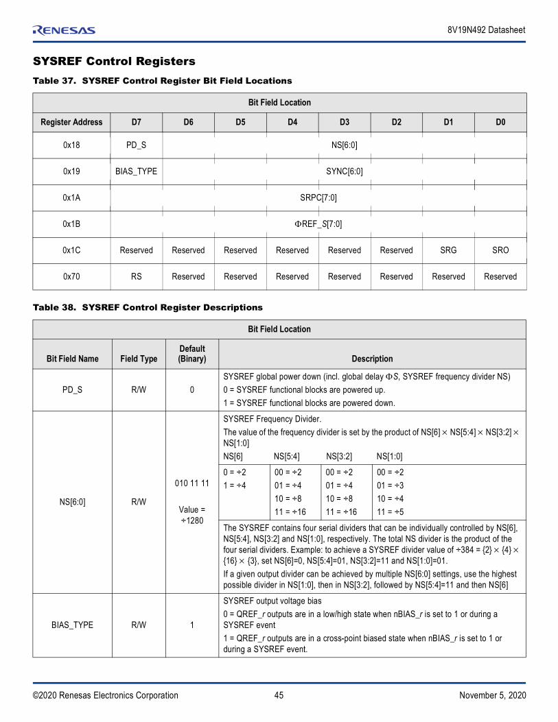
45©2020 Renesas Electronics Corporation November 5, 2020
8V19N492 Datasheet
SYSREF Control Registers Table 37. SYSREF Control Register Bit Field Locations
Bit Field Location
Register Address D7 D6 D5 D4 D3 D2 D1 D0
0x18 PD_S NS[6:0]
0x19 BIAS_TYPE SYNC[6:0]
0x1A SRPC[7:0]
0x1B REF_S[7:0]
0x1C Reserved Reserved Reserved Reserved Reserved Reserved SRG SRO
0x70 RS Reserved Reserved Reserved Reserved Reserved Reserved Reserved
Table 38. SYSREF Control Register Descriptions
Bit Field Location
Bit Field Name Field TypeDefault (Binary) Description
PD_S R/W 0SYSREF global power down (incl. global delay S, SYSREF frequency divider NS)0 = SYSREF functional blocks are powered up.1 = SYSREF functional blocks are powered down.
NS[6:0] R/W
010 11 11
Value = ÷1280
SYSREF Frequency Divider. The value of the frequency divider is set by the product of NS[6] NS[5:4] NS[3:2] NS[1:0]NS[6] NS[5:4] NS[3:2] NS[1:0]
0 = ÷21 = ÷4
00 = ÷201 = ÷410 = ÷811 = ÷16
00 = ÷201 = ÷410 = ÷811 = ÷16
00 = ÷201 = ÷310 = ÷411 = ÷5
The SYSREF contains four serial dividers that can be individually controlled by NS[6], NS[5:4], NS[3:2] and NS[1:0], respectively. The total NS divider is the product of the four serial dividers. Example: to achieve a SYSREF divider value of ÷384 = 2 4 16 3, set NS[6]=0, NS[5:4]=01, NS[3:2]=11 and NS[1:0]=01.If a given output divider can be achieved by multiple NS[6:0] settings, use the highest possible divider in NS[1:0], then in NS[3:2], followed by NS[5:4]=11 and then NS[6]
BIAS_TYPE R/W 1
SYSREF output voltage bias0 = QREF_r outputs are in a low/high state when nBIAS_r is set to 1 or during a SYSREF event1 = QREF_r outputs are in a cross-point biased state when nBIAS_r is set to 1 or during a SYSREF event.

46©2020 Renesas Electronics Corporation November 5, 2020
8V19N492 Datasheet
SYNC[6:0] R/W 00 00 001
SYSREF Synchronizer divider value. This divider controls the release of SYSREF pulses at coincident QCLK clock edges. For SYSREF operation, set this divider value to the least common multiple of the clock divider values Nx (x = A to E). For instance, if NA=NB=÷2, NC=ND=÷3, NE=÷4 set the SYNC divider to ÷12.SYNC6 Description0 = SYNC[6] = 0: output frequency divider set by SYNC[2:0]1 = SYNC[6] = 1: output frequency divider set by the product of SYNC[5:3] SYNC[2:0].
SYNC[5:3] SYNC[2:0]
000 = ÷2001 = ÷4010 = ÷6011 = ÷8100 = ÷4101 = ÷8110 = ÷12111 = ÷16
000 = ÷2001 = ÷3010 = ÷4011 = ÷5100 = ÷6101 = ÷7110 = ÷8111 = ÷9
The frequency divider SYNC is composed of 2 serial dividers that can be individually controlled by the bit fields SYNC[5:3] and SYNC[2:0].Set SYNC[6] = 0 to achieve an output divider in the range of 2,3,4,5,6,7,8,9Set SYNC[6] = 1 to achieve an output divider value of 2,4,6,8,12,16 2,3,4,5,6,7,8,9. For instance, the output divider of ÷32 = 4 8 is set by SYNC[6:0] = 1001110.If a given output divider can be achieved by multiple SYNC[6:0] settings, a setting with SYNC[6]=0 is preferred. If SNYC[6]=1, the higher divider value should be configured with SYNC[2:0].
SRPC[7:0] R/W0000 0010(value: 2)
SYSREF pulse countBinary value of the SYSREF pulses generated and output at all enabled QREF outputs. Allows to generate 1 to 255 pulses after each write access. Requires to set SRG = 0 and SRO = 0.
REF_S[7:0] R/W 00000
REF_S global SYSREF phase delay. This setting affects all QREF_r outputs configured as SYSREF.REF_S[7:0]
Delay in ps = REF_S 339ps (256 steps)0000 0000 = 0ps…1111 1111 = 86.466ns
Table 38. SYSREF Control Register Descriptions
Bit Field Location
Bit Field Name Field TypeDefault (Binary) Description

47©2020 Renesas Electronics Corporation November 5, 2020
8V19N492 Datasheet
Status Registers
SRG R/W 0SYSREF pulse generation0 = Internal, SPI controlled SYSREF generation using the RS bit.1 = External controlled SYSREF generation using the EXT_SYS pin.
SRO R/W 0
SYSREF pulse mode0 = Counted SYSREF pulse generation mode. Number of pulses is controlled by SRPC[7:0].1 = Continuous SYSREF pulse generation.
RSW only
Auto-ClearX
Set RS = 1 to initiate the SYSREF pulse generation of SRPC-number of pulses. Powers up the SYSREF circuitry and releases the SYSREF pulse(s) as configured.Requires SRG=0 and SRO=0, otherwise no function.RS = 1 also phase-aligns the QREF outputs to the QCLK outputs and adds the programmed delay values into the QREF paths.
Table 39. Status Register Bit Field Locations
Bit Field Location
Register Address D7 D6 D5 D4 D3 D2 D1 D0
0x68 Reserved Reserved IE_LOLF IE_LOLV Reserved Reserved IE_CLK_1 IE_CLK_0
0x69 Reserved Reserved Reserved Reserved Reserved Reserved IE_REF IE_HOLD
0x6C Reserved Reserved nLS_LOLF nLS_LOLV Reserved Reserved LS_CLK_1 LS_CLK_0
0x6D ST_SEL[1:0] nST_LOLF nST_LOLV Reserved Reserved ST_CLK_1 ST_CLK_0
0x6E Reserved Reserved Reserved Reserved Reserved Reserved LS_REF nLS_HOLD
0x6F Reserved Reserved Reserved Reserved Reserved ST_VCOF ST_REF nST_HOLD
Table 38. SYSREF Control Register Descriptions
Bit Field Location
Bit Field Name Field TypeDefault (Binary) Description

48©2020 Renesas Electronics Corporation November 5, 2020
8V19N492 Datasheet
Table 40. Status Register Descriptions[a]
Bit Field Location
Bit Field Name Field TypeDefault (Binary) Description
IE_LOLF R/W 0Interrupt Enable for FemtoClockNG-PLL loss of lock0 = Disabled: Setting LS_LOLF will not cause an interrupt on nINT1 = Enabled: Setting LS_LOLF will assert the nINT output (nINT=0, interrupt)
IE_LOLV R/W 0Interrupt Enable for VCXO-PLL loss of lock0 = Disabled: Setting LS_LOLV will not cause an interrupt on nINT1 = Enabled: Setting LS_LOLV will assert the nINT output (nINT=0, interrupt)
IE_CLK_n R/W 0Interrupt Enable for CLKn input loss-of-signal0 = Disabled: Setting LS_CLK_n will not cause an interrupt on nINT1 = Enabled: Setting LS_CLK_n will assert the nINT output (nINT=0, interrupt)
IE_REF R/W 0Interrupt Enable for LS_REF0 = Disabled: any changes to LS_REF will not cause an interrupt on nINT1 = Enabled: any changes to LS_REF will assert the nINT output (nINT=0, interrupt)
IE_HOLD R/W 0Interrupt Enable for holdover0 = Disabled: Setting LS_HOLD will not cause an interrupt on nINT1 = Enabled: Setting LS_HOLD will assert the nINT output (nINT=0, interrupt)
nLS_LOLF R/W -
FemtoClockNG-PLL loss of lock (latched status of nST_LOLF)Read 0 = 1 loss-of-lock events detected after the last status latch clearRead 1 = No loss-of-lock detected after the last status latch clearWrite 1 = Clear status latch (clears pending nLS_LOLF interrupt)
nLS_LOLV R/W -
VCXO-PLL loss of lock (latched status of nST_LOLV)Read 0 = 1 loss-of-lock events detected after the last status latch clear.Read 1 = No loss-of-lock detected after the last nLS_LOLV clearWrite 1 = Clear status latch (clears pending nLS_LOLV interrupt)
LS_CLK_n R/W -
Input CLK_n status (latched status of ST_CLK_n)Read 0 = 1 LOS events detected on CLK_n after the last LS_CLK_n clearRead 1 = No loss-of-signal detected on CLK_n input after the last LS_CLK_n clearWrite 1 = Clear LS_CLK_n status latch (clears pending LS_CLK_n interrupts on nINT)
ST_SEL[1:0] R -
Input selection (momentary status)Reference Input Selection Status of the state machine. In any input selection mode, reflects the input selected by the state machine.00 = CLK_001 = CLK_1
nST_LOLF R -
FemtoClockNG-PLL loss of lock (momentary status)Read 0 = 1 loss-of-lock events detectedRead 1 = No loss-of-lock detectedA latched version of these status bit is available (nLS_LOLF)

49©2020 Renesas Electronics Corporation November 5, 2020
8V19N492 Datasheet
nST_LOLV R -
VCXO-PLL loss of lock (momentary status bit)Read 0 = 1 loss-of-lock events detectedRead 1 = No loss-of-lock detectedA latched version of these status bits is available (nLS_LOLV)
ST_CLK_n R -
Input CLK_n status (momentary)0 = LOS detected on CLK_n1 = No LOS detected, CLK_n input is activeA latched version of these status bits are available (LS_CLK_n)
LS_REF R/W -
PLL reference status (latched status of ST_REF)Read 0 = Reference is lost since last reset of this status bit.Read 1 = Reference is valid since last reset of this status bit.Write 1 = Clear LS_REF status latch (clears pending IE_REF interrupts on nINT)
nLS_HOLD R/W
Holdover status indicator (latched status of ST_HOLD)Read 0 = VCXO-PLL has entered holdover state 1 times after reset of this status bitRead 1 = VCXO-PLL is (or attempts to) lock(ed) to an input clockWrite 1 = Clear status latch (clears pending nLS_HOLD interrupt)
ST_VCOF R -FemtoClockNG-PLL calibration status (momentary)Read 0 = FemtoClockNG PLL auto-calibration is completedRead 1 = FemtoClockNG PLL calibration is active (not completed)
ST_REF R -Input reference status0 = No input reference present1 = Input reference is present at the clock input selected by SEL[1:0]
nST_HOLD R -
Holdover status indicator (momentary)0 = VCXO-PLL in holdover state, not locked to any input clock1 = VCXO-PLL is (or attempts to) lock(ed) to input clockA latched version of this status bit is available (nLS_HOLD)
[a] CLKn = CLK0, CLK1, CLK2, CLK3.
Table 40. Status Register Descriptions[a]
Bit Field Location
Bit Field Name Field TypeDefault (Binary) Description

50©2020 Renesas Electronics Corporation November 5, 2020
8V19N492 Datasheet
General Control Registers Table 41. General Control Register Bit Field Locations
Bit Field Location
Register Address D7 D6 D5 D4 D3 D2 D1 D0
0x71 INIT_CLK Reserved Reserved Reserved Reserved Reserved Reserved Reserved
0x72 RELOCK Reserved Reserved Reserved Reserved Reserved Reserved Reserved
0x73 PB_CAL Reserved Reserved Reserved Reserved Reserved Reserved CPOL
Table 42. General Control Register Descriptions
Bit Field Location
Bit Field Name Field TypeDefault (Binary) Description
INIT_CLK W onlyAuto-Clear X Set INIT_CLK = 1 to initialize divider functions. Required as part of the startup
procedure.
RELOCK W onlyAuto-Clear X Setting this bit to 1 will force the FemtoClockNG PLL to re-lock.
PB_CAL W onlyAuto-Clear X
Precision Bias CalibrationSetting this bit to 1 will start the calibration of an internal precision bias current source. The bias current is used as reference for outputs configured as LVDS and for as reference for the charge pump currents. This bit will auto-clear after the calibration completed. Set as part of the startup procedure.
CPOL R/W 0SPI Read Operation SCLK Polarity0 = Data bits on SDAT are output at the falling edge of SCLK edge.1 = Data bits on SDAT are output at the rising edge of SCLK edge.

51©2020 Renesas Electronics Corporation November 5, 2020
8V19N492 Datasheet
Absolute Maximum RatingsThe absolute maximum ratings are stress ratings only. Stresses greater than those listed below can cause permanent damage to the device. Functional operation of the 8V19N492 at absolute maximum ratings is not implied. Exposure to absolute maximum rating conditions may affect device reliability.
Table 43. Absolute Maximum Ratings
Item Rating
Supply Voltage, VDD_V 3.6V
Inputs -0.5V to VDD_V + 0.5V
Outputs, VO (LVCMOS) -0.5V to VDD_V + 0.5V
Outputs, IO (LVPECL)Continuous CurrentSurge Current
50mA100mA
Outputs, IO (LVDS)Continuous CurrentSurge Current
50mA100mA
Input termination current, IVT ±35mA
Operating Junction Temperature, TJ 125C
Storage Temperature, TSTG -65C to 150C
ESD - Human Body Model[a]
[a] According to JEDEC JS-001-2012/JESD22-C101
2000V
ESD - Charged Device Modela 500V
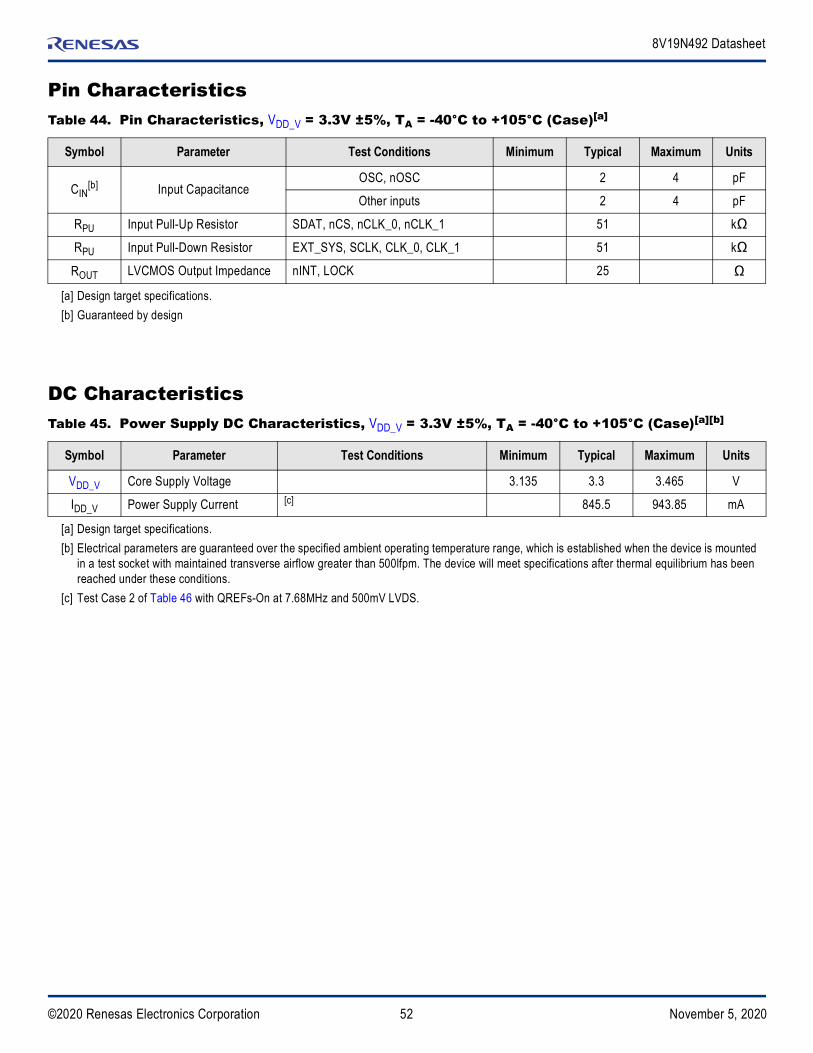
52©2020 Renesas Electronics Corporation November 5, 2020
8V19N492 Datasheet
Pin Characteristics
DC Characteristics
Table 44. Pin Characteristics, VDD_V = 3.3V ±5%, TA = -40°C to +105°C (Case)[a]
[a] Design target specifications.
Symbol Parameter Test Conditions Minimum Typical Maximum Units
CIN[b]
[b] Guaranteed by design
Input CapacitanceOSC, nOSC 2 4 pF
Other inputs 2 4 pF
RPU Input Pull-Up Resistor SDAT, nCS, nCLK_0, nCLK_1 51 kΩRPU Input Pull-Down Resistor EXT_SYS, SCLK, CLK_0, CLK_1 51 kΩ
ROUT LVCMOS Output Impedance nINT, LOCK 25 Ω
Table 45. Power Supply DC Characteristics, VDD_V = 3.3V ±5%, TA = -40°C to +105°C (Case)[a][b]
[a] Design target specifications.[b] Electrical parameters are guaranteed over the specified ambient operating temperature range, which is established when the device is mounted
in a test socket with maintained transverse airflow greater than 500lfpm. The device will meet specifications after thermal equilibrium has been reached under these conditions.
Symbol Parameter Test Conditions Minimum Typical Maximum Units
VDD_V Core Supply Voltage 3.135 3.3 3.465 V
IDD_V Power Supply Current [c]
[c] Test Case 2 of Table 46 with QREFs-On at 7.68MHz and 500mV LVDS.
845.5 943.85 mA

53©2020 Renesas Electronics Corporation November 5, 2020
8V19N492 Datasheet
Table 46. Typical Power Supply DC Current Characteristics, VDD_V = 3.3V ±5%, TA = -40°C to +105°C (Case)[a]
Symbol Supply Pin Current
Test Case
Unit1 2 3 4 5 6
QCLK_y
Style LVPECL LVPECL LVPECL LVPECL LVDS LVDSState On On On On On OnAmplitude 500 750 1000 250 500 750 mV
QREF_r Style LVDS LVDS LVDS LVDS LVDS LVDSState On On Off On Off OffAmplitude 500 500 250 mV
IDD_CA Current through VDD_QCLKA pin 85 101 113 75 69 85 mAIDD_CB Current through VDD_QCLKB pin 89 101 112 79 69 85 mAIDD_CC Current through VDD_QCLKC pin 64 69 75 58 53 61 mAIDD_CD Current through VDD_QCLKD pin 60 66 72 55 49 57 mAIDD_CE Current through VDD_QCLKE pin 91 102 113 80 69 85 mAIDD_RA Current through VDD_QREFA pin 77.3 77.1 0 55.7 0 0 mAIDD_RB Current through VDD_QREFB pin 51.3 51.3 0 36.9 0 0 mAIDD_RC Current through VDD_QREFC pin 27.3 25.3 0 20.9 0 0 mAIDD_RD Current through VDD_QREFD pin 26.1 25.9 0 18.7 0 0 mAIDD_INP Current through VDD_INP pin 60.50 61 61.8 60.1 62.6 63.3 mAIDD_SPI Current through VDD_SPI pin 6.0 6.5 6.4 4.4 5.9 6.0 mA
IDD_OSC + IDD_CP
Current through VDD_OSC and VDD_CP pins 38.7 38.8 38.9 38.6 39.3 39.0 mA
IDD_SYNC Current through VDD_SYNC pin 82.6 82.6 1.9 82.8 1.9 1.9 mAIDD_CPF Current through VDD_CPF pin 59.4 59.5 59.4 59.4 59.4 60.2 mAIDD_LCV Current through VDD_LCV pin 72.3 72.3 72.2 72.3 74.4 76.9 mAIDD_LCF Current through VDD_LCF pin 52.2 52.0 52.5 52.5 52.4 52.4 mA
PTOT Total Device Power Consumption 2.7 2.8 2.0 2.5 2.0 2.2 WPTOT, SYS Total System Power Consumption[b] 3.1 3.3 2.6 2.8 2.0 2.2 W
[a] Configuration: fCLK (input) = 122.88MHz, fSYSREF=7.68MHz, internal SYSREF generation (continuous), QA[2:0] = 1474.56MHz, QB[1:0] = 245.76MHz, QC[1:0] = 245.76MHz, QD = 491.52MHz, QE[1:0] = 122.88MHz). QCLK_y outputs terminated according to amplitude settings. QREF_r outputs unterminated when SYSREF is turned off.
[b] Includes total device power consumption and the power dissipated in external output termination components.

54©2020 Renesas Electronics Corporation November 5, 2020
8V19N492 Datasheet
Table 47. LVCMOS DC Characteristics, VDD_V = 3.3V ±5%, TA = -40°C to +85°C
Symbol Parameter Test Conditions Minimum Typical Maximum Units
Control Input SELSV (3.3V Logic)VIH Input High Voltage 2.0 VDD_V VVIL Input Low Voltage -0.3 0.8 VIIH Input High Current VDD_V = 3.3V, VIN = 3.3V 150 µAIIL Input Low Current VDD_V = 3.3V, VIN = 0V -5 µA
SYSREF Trigger Input EXT_SYS (1.8V/3.3V Selectable Logic)
VIH Input High Voltage1.8V logic (SELSV = 0) 1.17 VDD_V V3.3V logic (SELSV = 1) 2.0 VDD_V V
VIL Input Low Voltage1.8V logic (SELSV = 0) -0.3 0.63 V3.3V logic (SELSV = 1) -0.3 0.8 V
IIH Input High Current VDD_V = 3.3V, VIN = 1.8V or 3.3V 150 µA
IIL Input Low Current VDD_V = 3.3V, VIN = 0V -5 µASPI Inputs SDAT (when input), SCLK, nCS (1.8V/3.3V Selectable Logic with Input Hysteresis)
VI Input Voltage -0.3 VDD_V V
VT+ Positive-going Input Threshold Voltage1.8V logic (SELSV = 0) 0.660 1.350 V3.3V logic (SELSV = 1) 1.8–2.1 V
VT- Negative-going Input Threshold Voltage1.8V logic (SELSV = 0) 0.495 1.170 V3.3V logic (SELSV = 1) 0.75–0.97 V
VH Hysteresis Voltage VT+ – VT- 0.165 0.780 V
IIHInputHigh Current
Inputs with pull-down resistor[a]
VDD_V = 3.3V, VIH = 1.8V150
µAInputs with pull-up resistor[b] 5
IILInputLow Current
Inputs with pull-down resistor[a]
VDD_V = 3.465V, VIL = 0V-5
µAInputs with pull-up resistor[b] -150
SPI output DAT (when output), nINT, LOCK (1.8V/3.3V selectable logic)
VOH Output High Voltage
1.8V logic (SELSV = 0)IOH = -4mA
1.35 V
3.3V logic (SELSV = 1)IOH = -4mA
2.4 V
VOL Output Low Voltage
1.8V logic (SELSV = 0)IOL = 4mA
0.45 V
3.3V logic (SELSV = 1)IOL = 4mA
0.4 V
[a] SCLK, EXT_SYS. [b] nCS, SDAT (when input)
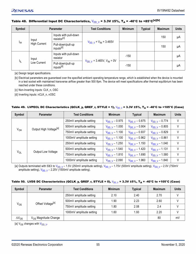
55©2020 Renesas Electronics Corporation November 5, 2020
8V19N492 Datasheet
Table 48. Differential Input DC Characteristics, VDD_V = 3.3V ±5%, TA = -40°C to +85°C[a][b]
Symbol Parameter Test Conditions Minimum Typical Maximum Units
IIHInputHigh Current
Inputs with pull-down resistor[c]
VDD_V = VIN = 3.465V150 µA
Pull-down/pull-up inputs[d] 150 µA
IILInputLow Current
Inputs with pull-down resistor
VDD_V = 3.465V, VIN = 0V-150 µA
Pull-down/pull-up inputs[d] -150 µA
[a] Design target specifications.[b] Electrical parameters are guaranteed over the specified ambient operating temperature range, which is established when the device is mounted
in a test socket with maintained transverse airflow greater than 500 lfpm. The device will meet specifications after thermal equilibrium has been reached under these conditions.
[c] Non-Inverting inputs: CLK_n, OSC[d] Inverting inputs: nCLK_n, nOSC
Table 49. LVPECL DC Characteristics (QCLK_y, QREF_r, STYLE = 1), VDD_V = 3.3V ±5%, TA = -40°C to +105°C (Case)
Symbol Parameter Test Conditions Minimum Typical Maximum Units
VOH Output High Voltage[a]
[a] Outputs terminated with 50 to VDD_V – 1.5V (250mV amplitude setting), VDD_V – 1.75V (500mV amplitude setting), VDD_V – 2.0V (750mV amplitude setting), VDD_V – 2.25V (1000mV amplitude setting).
250mV amplitude setting VDD_V – 0.975 VDD_V – 0.875 VDD_V – 0.774 V
500mV amplitude setting VDD_V – 1.000 VDD_V – 0.904 VDD_V – 0.805 V
750mV amplitude setting VDD_V – 1.100 VDD_V – 0.937 VDD_V – 0.829 V
1000mV amplitude setting VDD_V – 1.100 VDD_V – 0.962 VDD_V – 0.861 V
VOL Output Low Voltage
250mV amplitude setting VDD_V – 1.250 VDD_V – 1.150 VDD_V – 1.040 V
500mV amplitude setting VDD_V – 1.540 VDD_V – 1.420 VDD_V – 1.131 V
750mV amplitude setting VDD_V – 1.810 VDD_V – 1.690 VDD_V – 1.580 V
1000mV amplitude setting VDD_V – 2.090 VDD_V – 1.960 VDD_V – 1.840 V
Table 50. LVDS DC Characteristics (QCLK_y, QREF_r, STYLE = 0), VDD_V = 3.3V ±5%, TA = -40°C to +105°C (Case)
Symbol Parameter Test Conditions Minimum Typical Maximum Units
VOS Offset Voltage[a]
[a] VOS changes with VDD_V.
250mV amplitude setting 2.10 2.40 2.70 V
500mV amplitude setting 1.90 2.23 2.60 V
750mV amplitude setting 1.80 2.08 2.4 V
1000mV amplitude setting 1.60 1.93 2.20 V
VOS VOS Magnitude Change 80 mV

56©2020 Renesas Electronics Corporation November 5, 2020
8V19N492 Datasheet
AC CharacteristicsTable 51. AC Characteristics, VDD_V = 3.3V ±5%, TA = -40°C to +105°C (Case)[a][b][c]
Symbol Parameter Test Conditions Minimum Typical Maximum Units
fVCO VCO Frequency 2920 2949.12 3000 MHz
fOUT Output Frequency
QCLK_y, QREF_r (Clock), N=÷1 2949.12 MHz
QCLK_y, QREF_r (Clock), N=÷2 1474.56 MHz
QCLK_y, QREF_r (Clock), N=÷3 983.04 MHz
QCLK_y, QREF_r (Clock), N=÷6 491.52 MHz
QCLK_y, QREF_r (Clock), N=÷12 245.76 MHz
QCLK_y, QREF_r (Clock), N=÷24 122.88 MHz
QREF_r (SYSREF) 0.576 30.72 MHz
fCLK Input Frequency CLK_n 1.92[d] 245.76 2000 MHz
fVCXO VCXO Frequency 30.72 122.88 500 MHz
Δfp Static Frequency Error fCLK = 0pbb frequency deviation 0 ppb
ΔfrmsDynamic Frequency Error RMS[e]
fCLK = 0ppb frequency deviation 0.5 ppb
VIN Input Voltage Amplitude[f] CLK_n, nCLK_n 0.15 1.2 V
VDIFF_INDifferential Input Voltage Amplitude[f][g]
CLK_n - nCLK_n 0.3 2.4 V
VCMR Common Mode Input Voltage 1.0 VDD_V – (VIN / 2)
V
odc Output Duty Cycle QCLK_y, QREF_r (Clock) 45 50 55 %
tR / tFOutput Rise/Fall Time, Differential
QCLK_y, QREF_r (LVPECL), 20–80% 250 ps
QCLK_y, QREF_r (LVDS), 20–80% 250 ps
QREF_r (SYSREF, LVDS), 20–80% 250 ps
Output Rise/Fall Time LVCMOS outputs, 20%-80% 1 ns
VO(PP)[h]
LVPECL Output Voltage Swing, Peak-to-peak, 1474.56MHz
250mV Amplitude Setting 190 272 367 mV
500mV Amplitude Setting 394 505 634 mV
750mV Amplitude Setting 598 733 875 mV
1000mV Amplitude Setting 784 946 1090 mV
LVPECL Differential Output Voltage Swing, Peak-to-peak, 1474.56MHz
250mV Amplitude Setting 380 544 734 mV
500mV Amplitude Setting 788 1010 1268 mV
750mV Amplitude Setting 1196 1466 1750 mV
1000mV Amplitude Setting 1585 1892 2180 mV

57©2020 Renesas Electronics Corporation November 5, 2020
8V19N492 Datasheet
VOD[i]
LVDS Output Voltage Swing, Peak-to-peak, 1474.56MHz
250mV Amplitude Setting 128 193 273 mV
500mV Amplitude Setting 312 404 512 mV
750mV Amplitude Setting 490 615 757 mV
1000mV Amplitude Setting 676 822 992 mV
LVDS Differential Output Voltage Swing, Peak-to-peak, 1474.56MHz
250mV Amplitude Setting 256 386 546 mV
500mV Amplitude Setting 624 808 1024 mV
750mV Amplitude Setting 980 1230 1514 mV
1000mV Amplitude Setting 1352 1644 1984 mV
ΔtPD
Propagation delay variation between reference input and any QCLK_y output
-200 +200 ps
tsk(o)Output Skew[j][k]
All delays set to 0
QCLK_y (same N divider) 100 ps
QCLK_y (any N divider, incident rising edge) 100 ps
QREF_r (Clock) 100 ps
QREF_r (SYSREF) 100 ps
QREF_r (Clock) to QCLK_y (any divider, incident rising QCLK edge)
150 ps
QREF_r (SYSREF) to QCLK_y (any divider, incident rising QCLK edge)
150 ps
ΔΦ Output isolation between any neighboring clock output
fOUT = 983.04MHz 77 dB
fOUT = 491.52MHz 65 83 dB
fOUT = 245.76MHz 70 86 dB
ΔΦOutput isolation between any QCLK_y, QREF_r (SYSREF[l]) output
Both SYSREF and clock signals active 50 60 dB
tD, LOSLOS state detected (Measured in input reference periods)
fIN = 122.88MHz 2TINfIN = 245.76MHz 3
tD, LOCK PLL lock detect
PLL re-lock time after a short-term holdover scenario. Measured from LOS to both PLLs lock-detect asserted; hold-off timer = 200ms, initial frequency error <200 ppm. PLL1 BW 100HzPLL1 BW 30Hz
42100
300300
ms
tD, RES PLL lock residual time error
Refer to PLL lock detect tD,LOCK. Reference point: final value of clock output phase after all phase transitions settled.PLL1 BW 100HzPLL1 BW 30Hz
0.00990.0019
2020
ns
Table 51. AC Characteristics, VDD_V = 3.3V ±5%, TA = -40°C to +105°C (Case)[a][b][c]
Symbol Parameter Test Conditions Minimum Typical Maximum Units

58©2020 Renesas Electronics Corporation November 5, 2020
8V19N492 Datasheet
ΔfHOLD Holdover accuracy
Max. frequency deviation during a holdover duration of 200ms and after the clock re-validate eventPLL1 BW 100HzPLL1 BW 30Hz
1.620.5
±5±5
ppm
tD, RES-H Holdover residual error.
Measured 50ms after the reference clock re-appeared in a holdover scenario. Reference point: final value of clock output phase after all phase transitions settled.PLL1 BW 100HzPLL1 BW 30Hz
4.324.63
±8.138±8.138
ns
tH Hold Time EXT_SYS to CLK_n[m] 2.5 ns
tS Setup Time EXT_SYS to CLK_n[m] 0 ns
tW Pulse Width EXT_SYS[m] 4 ns
[a] Design target specifications.[b] Electrical parameters are guaranteed over the specified ambient operating temperature range, which is established when the device is mounted
in a test socket with maintained transverse airflow greater than 500 lfpm. The device will meet specifications after thermal equilibrium has been reached under these conditions.
[c] VCXO-PLL bandwidth = 100Hz.[d] Minimum input frequency for the loss the input reference detector is fVCO/MV1(MAX)[e] RMS frequency error, measured at any QCLK_y output, caused by Gaussian noise. Weighted with a 1ms low pass time window filter.[f] VIL should not be less than -0.3V and VIH should not be greater than VDD_V [g] Common Mode Input Voltage is defined as the cross-point voltage.[h] LVPECL outputs terminated with 50 to VCCO – 1.5V (250mV amplitude setting), VCCO – 1.75V (500mV amplitude setting), VCCO – 2.0V (750mV
amplitude setting), VCCO – 2.25V (1000mV amplitude setting)[i] LVDS outputs terminated 100 across terminals[j] This parameter is defined in accordance with JEDEC standard 65[k] Defined as skew between outputs at the same supply voltage and with equal load conditions. Measured at the differential cross points[l] SYSREF frequencies: 30.72, 15.36, 7.68MHz[m]SYSREF external trigger mode, BYPV = 0, BYPF = 1 (PLL feedback through MV0 and MV1), PV0 = ÷1024, MV0 = ÷1024, MV1 = ÷12, NS = ÷384,
SYNC = ÷12, fIN = 245.76MHz (see Figure 8).
Table 51. AC Characteristics, VDD_V = 3.3V ±5%, TA = -40°C to +105°C (Case)[a][b][c]
Symbol Parameter Test Conditions Minimum Typical Maximum Units
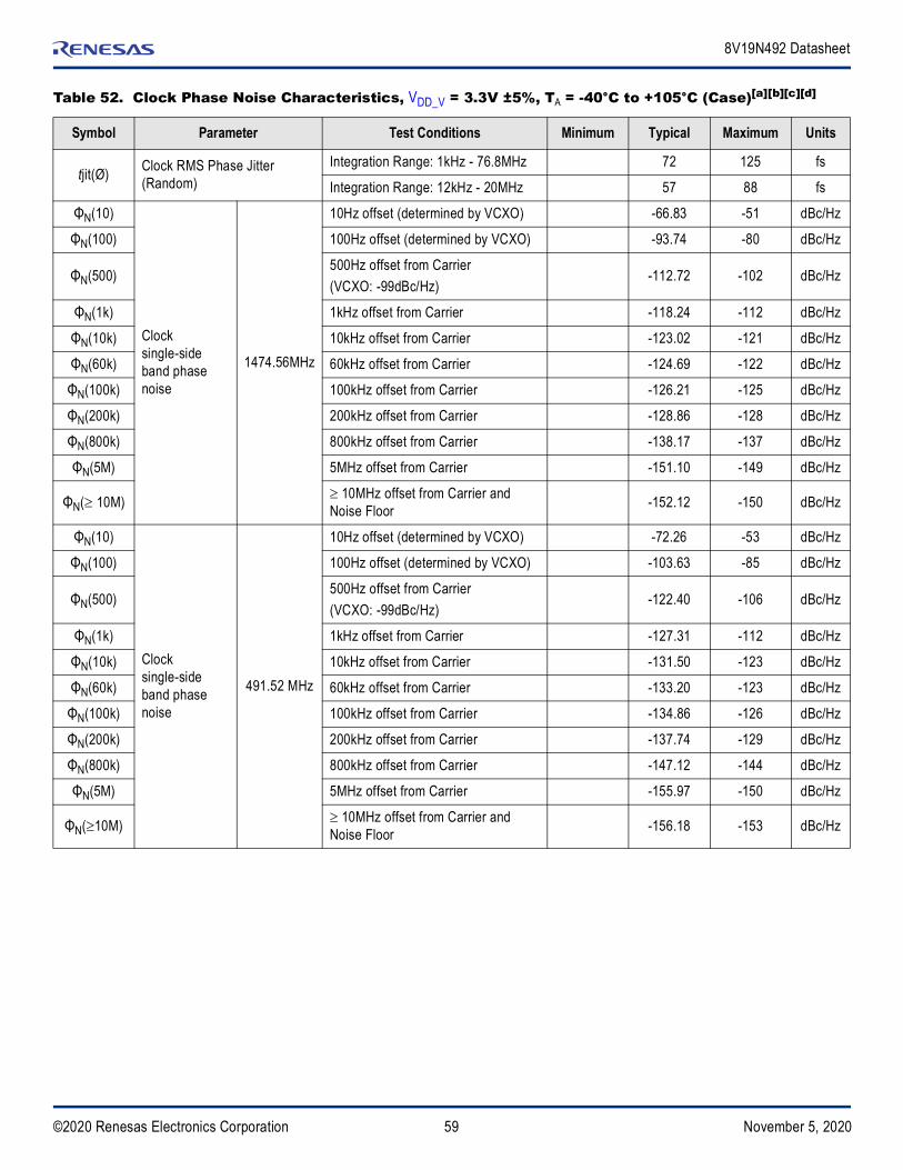
59©2020 Renesas Electronics Corporation November 5, 2020
8V19N492 Datasheet
Table 52. Clock Phase Noise Characteristics, VDD_V = 3.3V ±5%, TA = -40°C to +105°C (Case)[a][b][c][d]
Symbol Parameter Test Conditions Minimum Typical Maximum Units
tjit(Ø) Clock RMS Phase Jitter (Random)
Integration Range: 1kHz - 76.8MHz 72 125 fs
Integration Range: 12kHz - 20MHz 57 88 fs
ΦN(10)
Clock single-side band phase noise
1474.56MHz
10Hz offset (determined by VCXO) -66.83 -51 dBc/Hz
ΦN(100) 100Hz offset (determined by VCXO) -93.74 -80 dBc/Hz
ΦN(500)500Hz offset from Carrier(VCXO: -99dBc/Hz)
-112.72 -102 dBc/Hz
ΦN(1k) 1kHz offset from Carrier -118.24 -112 dBc/Hz
ΦN(10k) 10kHz offset from Carrier -123.02 -121 dBc/Hz
ΦN(60k) 60kHz offset from Carrier -124.69 -122 dBc/Hz
ΦN(100k) 100kHz offset from Carrier -126.21 -125 dBc/Hz
ΦN(200k) 200kHz offset from Carrier -128.86 -128 dBc/Hz
ΦN(800k) 800kHz offset from Carrier -138.17 -137 dBc/Hz
ΦN(5M) 5MHz offset from Carrier -151.10 -149 dBc/Hz
ΦN( 10M) 10MHz offset from Carrier and Noise Floor -152.12 -150 dBc/Hz
ΦN(10)
Clock single-side band phase noise
491.52 MHz
10Hz offset (determined by VCXO) -72.26 -53 dBc/Hz
ΦN(100) 100Hz offset (determined by VCXO) -103.63 -85 dBc/Hz
ΦN(500)500Hz offset from Carrier(VCXO: -99dBc/Hz)
-122.40 -106 dBc/Hz
ΦN(1k) 1kHz offset from Carrier -127.31 -112 dBc/Hz
ΦN(10k) 10kHz offset from Carrier -131.50 -123 dBc/Hz
ΦN(60k) 60kHz offset from Carrier -133.20 -123 dBc/Hz
ΦN(100k) 100kHz offset from Carrier -134.86 -126 dBc/Hz
ΦN(200k) 200kHz offset from Carrier -137.74 -129 dBc/Hz
ΦN(800k) 800kHz offset from Carrier -147.12 -144 dBc/Hz
ΦN(5M) 5MHz offset from Carrier -155.97 -150 dBc/Hz
ΦN(10M) 10MHz offset from Carrier and Noise Floor -156.18 -153 dBc/Hz
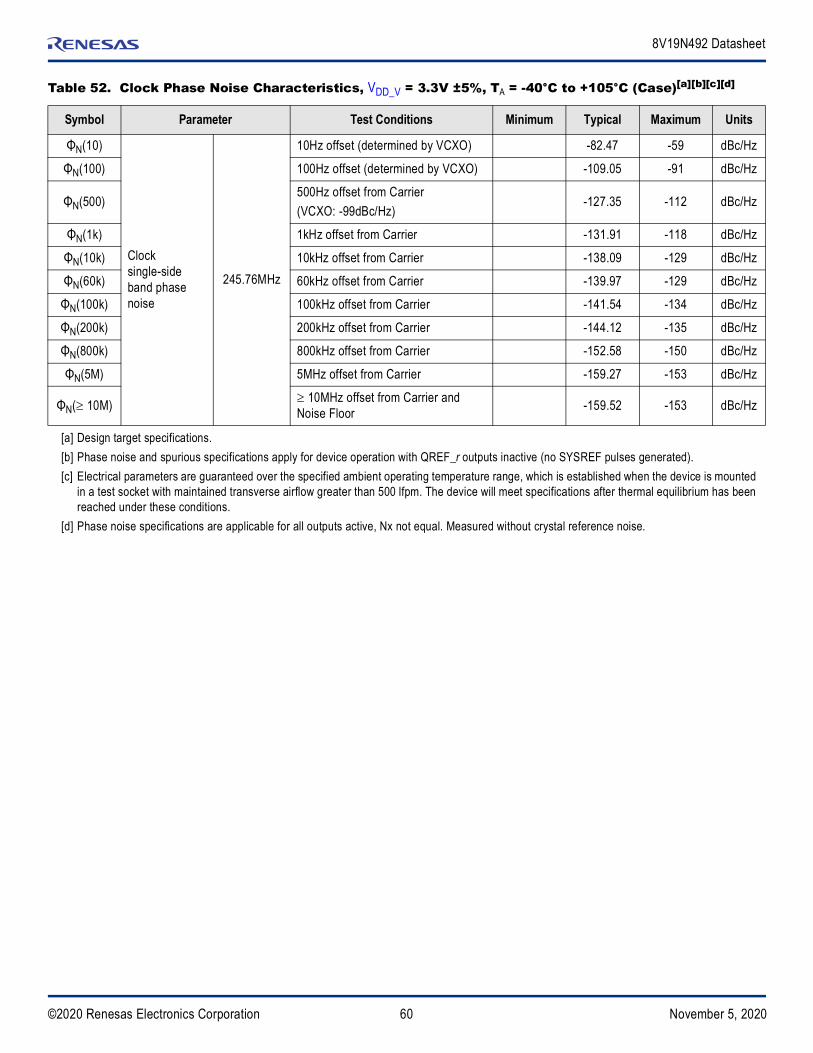
60©2020 Renesas Electronics Corporation November 5, 2020
8V19N492 Datasheet
ΦN(10)
Clock single-side band phase noise
245.76MHz
10Hz offset (determined by VCXO) -82.47 -59 dBc/Hz
ΦN(100) 100Hz offset (determined by VCXO) -109.05 -91 dBc/Hz
ΦN(500)500Hz offset from Carrier (VCXO: -99dBc/Hz)
-127.35 -112 dBc/Hz
ΦN(1k) 1kHz offset from Carrier -131.91 -118 dBc/Hz
ΦN(10k) 10kHz offset from Carrier -138.09 -129 dBc/Hz
ΦN(60k) 60kHz offset from Carrier -139.97 -129 dBc/Hz
ΦN(100k) 100kHz offset from Carrier -141.54 -134 dBc/Hz
ΦN(200k) 200kHz offset from Carrier -144.12 -135 dBc/Hz
ΦN(800k) 800kHz offset from Carrier -152.58 -150 dBc/Hz
ΦN(5M) 5MHz offset from Carrier -159.27 -153 dBc/Hz
ΦN( 10M) 10MHz offset from Carrier and Noise Floor -159.52 -153 dBc/Hz
[a] Design target specifications.[b] Phase noise and spurious specifications apply for device operation with QREF_r outputs inactive (no SYSREF pulses generated).[c] Electrical parameters are guaranteed over the specified ambient operating temperature range, which is established when the device is mounted
in a test socket with maintained transverse airflow greater than 500 lfpm. The device will meet specifications after thermal equilibrium has been reached under these conditions.
[d] Phase noise specifications are applicable for all outputs active, Nx not equal. Measured without crystal reference noise.
Table 52. Clock Phase Noise Characteristics, VDD_V = 3.3V ±5%, TA = -40°C to +105°C (Case)[a][b][c][d]
Symbol Parameter Test Conditions Minimum Typical Maximum Units

61©2020 Renesas Electronics Corporation November 5, 2020
8V19N492 Datasheet
Table 53. Clock Spurious Signals Characteristics, VDD_V = 3.3V ±5%, TA = -40°C to +105°C (Case) [a] [b]
Symbol Parameter Test Conditions Minimum Typical Maximum Units
ΦSpurious Signals(QCLK, QREF as clock)
983.04MHz
100Hz–300Hz -75.6 -67.5 dBc
300Hz–100kHz -101.0 -90.3 dBc
100kHz–100MHz -93.7 -86.2 dBc
122.88MHz reference spurious[c] -77.8 -70 dBc
245.76MHz reference spurious[d] -84.6 -70 dBc
491.52MHz reference spurious[e] -78.3 -65 dBc
491.52MHz
100Hz–300Hz -82.1 -74.9 dBc
300Hz–100kHz -97.9 -86.1 dBc
100kHz–100MHz -92.7 -84.7 dBc
122.88MHz reference spurious[c] -92.2 -70 dBc
245.76MHz reference spurious[d] -84 -70 dBc
245.76MHz
100Hz–300Hz -87.6 -80.3 dBc
300Hz–100kHz -109.0 -102.2 dBc
100kHz–100MHz -90.9 -87.9 dBc
122.88MHz reference spurious[c] -86.7 -70 dBc
[a] Spurious specifications apply for device operation with QREF_r outputs inactive (no SYSREF pulses generated). [b] Electrical parameters are guaranteed over the specified ambient operating temperature range, which is established when the device is mounted
in a test socket with maintained transverse airflow greater than 500lfpm. The device will meet specifications after thermal equilibrium has been reached under these conditions.
[c] Measured at all offset frequencies except at fOFFSET = 122.88MHz.[d] Measured at all offset frequencies except at fOFFSET = 245.76MHz.[e] Measured at all offset frequencies except at fOFFSET = 491.52MHz.

62©2020 Renesas Electronics Corporation November 5, 2020
8V19N492 Datasheet
Table 54. SYSREF Phase Noise Characteristics, VDD_V = 3.3V ±5%, TA = -40°C to +105°C (Case)[a][b][c]
Symbol Parameter Test Conditions Minimum Typical Maximum Units
ΦN(500)
SYSREF single-side band phase noise
30.72 MHz
500Hz offset -144.58 -130 dBc/Hz
ΦN(10k) 10kHz offset from Carrier -154.66 -130 dBc/Hz
ΦN(60k) 60kHz offset from Carrier -155.10 -140 dBc/Hz
ΦN(800k) 800kHz offset from Carrier -158.13 -145 dBc/Hz
ΦN(3M) 3MHz offset from Carrier and Noise Floor -158.11 -145 dBc/Hz
ΦN(500)
SYSREF single-side band phase noise
15.36 MHz
500Hz offset -148.16 -130 dBc/Hz
ΦN(10k) 10kHz offset from Carrier -157.15 -130 dBc/Hz
ΦN(60k) 60kHz offset from Carrier -158.24 -140 dBc/Hz
ΦN(800k) 800kHz offset from Carrier -159.62 -145 dBc/Hz
ΦN(3M) 3 MHz offset from Carrier and Noise Floor -159.63 -145 dBc/Hz
ΦN(500)
SYSREF single-side band phase noise
7.68 MHz
500Hz offset -138.09 -130 dBc/Hz
ΦN(10k) 10kHz offset from Carrier -148.86 -130 dBc/Hz
ΦN(60k) 60kHz offset from Carrier -158.12 -140 dBc/Hz
ΦN(800k) 800kHz offset from Carrier -145 dBc/Hz
ΦN( 3M) 3MHz offset from Carrier and Noise Floor -145 dBc/Hz
Φ Spurious signals[d]
30.72MHz > 500Hz -60 -56 dBc
15.36MHz > 500Hz -60 -56 dBc
7.68MHz > 500Hz -60 -56 dBc
[a] Design target specifications.[b] Phase noise is measured as additive phase noise contribution by the device on all SYSREF outputs, dividers and channel logic. SYSREF signals
measured as continued clock signal. Clock signals (QCLK) are turned on.[c] Electrical parameters are guaranteed over the specified ambient operating temperature range, which is established when the device is mounted
in a test socket with maintained transverse airflow greater than 500 lfpm. The device will meet specifications after thermal equilibrium has been reached under these conditions.
[d] Measured as sum of all spurious amplitudes in one side band in the offset frequency range above 500Hz, excluding the harmonics of the fundamental frequency of n*fSYSREF (e.g., n*7.68MHz)).

63©2020 Renesas Electronics Corporation November 5, 2020
8V19N492 Datasheet
Figure 8. EXT_SYS Input Timing Diagram
Clock Phase Noise CharacteristicsConditions for Phase Noise Characteristics:
VCXO characteristics: f=122.88 MHz and phase noise: -85dBc/Hz(10Hz), -115dBc/Hz(100Hz), -145dBc/Hz(1kHz),-155dBc/Hz(10kHz), -160dBc/Hz(100kHz)
Input reference frequency: 122.88MHz VCXO-PLL bandwidth: 27Hz VCXO-PLL charge pump current: 0.75mA FemtoClock-NG PLL bandwidth: 139kHz VDD_V = 3.3V, TA = 25oC
Table 55. AC Characteristics: Typical QCLK_y Output Amplitude, VDD_V = 3.3V, TA = 85°C[a]
Symbol Parameter Test Conditions
QCLK_y Output Frequency in MHz
Units2949.12 1474.56 983.04 737.28 491.52 245.76
VO(PP)[b]
LVPECL Output Voltage Swing, Peak-to-peak
250mV Amplitude Setting 214 283 260 262 264 281 mV
500mV Amplitude Setting 376 520 492 484 508 520 mV
750mV Amplitude Setting 512 748 740 716 730 768 mV
1000mV Amplitude Setting 628 960 984 944 968 1008 mV
VOD[c]
LVDS Output Voltage Swing, Peak-to-peak
250mV Amplitude Setting 120 190 200 210 215 225 mV
500mV Amplitude Setting 250 390 410 430 440 470 mV
750mV Amplitude Setting 370 592 650 670 682 710 mV
1000mV Amplitude Setting 475 790 870 900 920 980 mV
[a] Electrical parameters are guaranteed over the specified ambient operating temperature range, which is established when the device is mounted in a test socket with maintained transverse airflow greater than 500 lfpm. The device will meet specifications after thermal equilibrium has been reached under these conditions.
[b] LVPECL outputs terminated with 50 to VDD_V – 1.5V (250mV amplitude setting), VDD_V – 1.75V (500mV amplitude setting), VDD_V – 2.0V (750mV amplitude setting), VCCO – 2.25V (1000mV amplitude setting)
[c] LVDS outputs terminated 100 across terminals
CLK_n
EXT_SYS
QREF_r High Impedance
tS tH
Valid EXT_SYStW
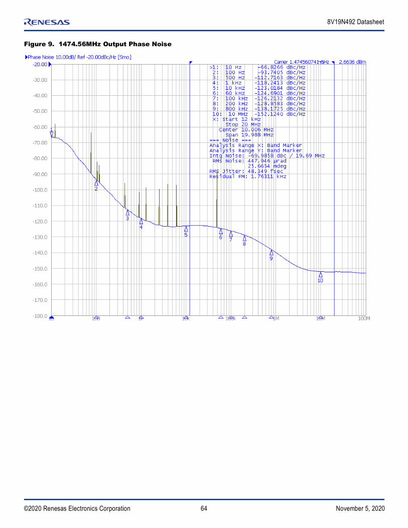
64©2020 Renesas Electronics Corporation November 5, 2020
8V19N492 Datasheet
Figure 9. 1474.56MHz Output Phase Noise

65©2020 Renesas Electronics Corporation November 5, 2020
8V19N492 Datasheet
Figure 10. 491.52MHz Output Phase Noise
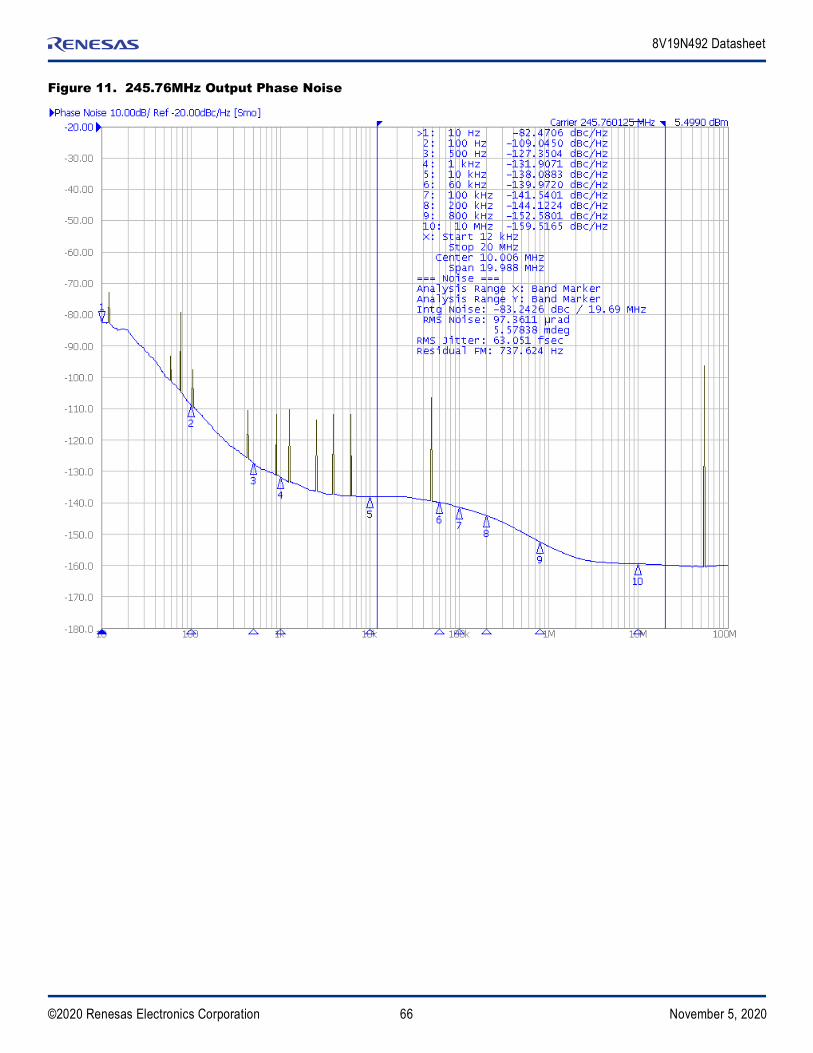
66©2020 Renesas Electronics Corporation November 5, 2020
8V19N492 Datasheet
Figure 11. 245.76MHz Output Phase Noise
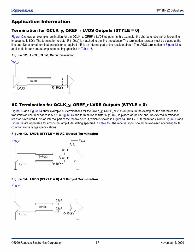
67©2020 Renesas Electronics Corporation November 5, 2020
8V19N492 Datasheet
Application Information
Termination for QCLK_y, QREF_r LVDS Outputs (STYLE = 0)Figure 12 shows an example termination for the QCLK_y, QREF_r LVDS outputs. In this example, the characteristic transmission line impedance is 50. The termination resistor R (100) is matched to the line impedance. The termination resistor must be placed at the line end. No external termination resistor is required if R is an internal part of the receiver circuit. The LVDS termination in Figure 12 is applicable for any output amplitude setting specified in Table 15.
Figure 12. LVDS (SYLE=0) Output Termination
AC Termination for QCLK_y, QREF_r LVDS Outputs (STYLE = 0)Figure 13 and Figure 14 show example AC terminations for the QCLK_y, QREF_r LVDS outputs. In the examples, the characteristic transmission line impedance is 50. In Figure 13, the termination resistor R (100) is placed at the line end. No external termination resistor is required if R is an internal part of the receiver circuit, which is shown in Figure 14. The LVDS terminations in both Figure 13 and Figure 14 are applicable for any output amplitude setting specified in Table 15. The receiver input should be re-biased according to its common mode range specifications.
Figure 13. LVDS (STYLE = 0) AC Output Termination
Figure 14. LVDS (STYLE = 0) AC Output Termination
R=100
VDD_V
LVDS
T=50
VDD_V
LVDS
T=50 0.1µF
0.1µF
R=100
VBIAS
VDD_V
LVDS
T=50 0.1µF
0.1µF
R=100
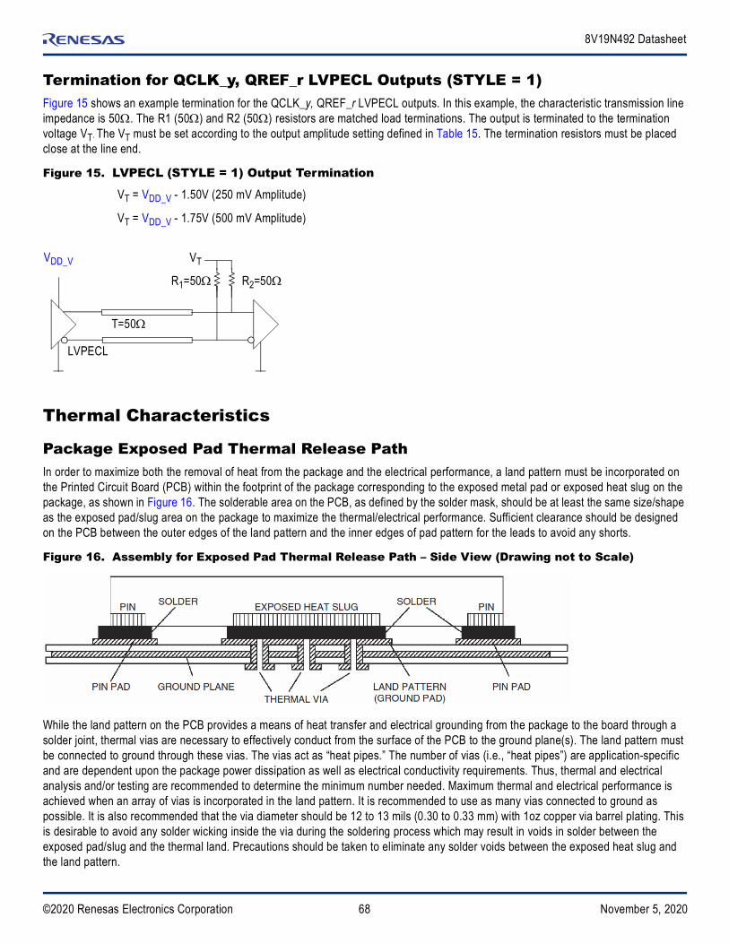
68©2020 Renesas Electronics Corporation November 5, 2020
8V19N492 Datasheet
Termination for QCLK_y, QREF_r LVPECL Outputs (STYLE = 1)Figure 15 shows an example termination for the QCLK_y, QREF_r LVPECL outputs. In this example, the characteristic transmission line impedance is 50. The R1 (50) and R2 (50)resistors are matched load terminations. The output is terminated to the termination voltage VT. The VT must be set according to the output amplitude setting defined in Table 15. The termination resistors must be placed close at the line end.
Figure 15. LVPECL (STYLE = 1) Output Termination
Thermal Characteristics
Package Exposed Pad Thermal Release PathIn order to maximize both the removal of heat from the package and the electrical performance, a land pattern must be incorporated on the Printed Circuit Board (PCB) within the footprint of the package corresponding to the exposed metal pad or exposed heat slug on the package, as shown in Figure 16. The solderable area on the PCB, as defined by the solder mask, should be at least the same size/shape as the exposed pad/slug area on the package to maximize the thermal/electrical performance. Sufficient clearance should be designed on the PCB between the outer edges of the land pattern and the inner edges of pad pattern for the leads to avoid any shorts.
Figure 16. Assembly for Exposed Pad Thermal Release Path – Side View (Drawing not to Scale)
While the land pattern on the PCB provides a means of heat transfer and electrical grounding from the package to the board through a solder joint, thermal vias are necessary to effectively conduct from the surface of the PCB to the ground plane(s). The land pattern must be connected to ground through these vias. The vias act as “heat pipes.” The number of vias (i.e., “heat pipes”) are application-specific and are dependent upon the package power dissipation as well as electrical conductivity requirements. Thus, thermal and electrical analysis and/or testing are recommended to determine the minimum number needed. Maximum thermal and electrical performance is achieved when an array of vias is incorporated in the land pattern. It is recommended to use as many vias connected to ground as possible. It is also recommended that the via diameter should be 12 to 13 mils (0.30 to 0.33 mm) with 1oz copper via barrel plating. This is desirable to avoid any solder wicking inside the via during the soldering process which may result in voids in solder between the exposed pad/slug and the thermal land. Precautions should be taken to eliminate any solder voids between the exposed heat slug and the land pattern.
R1=50 R2=50
VDD_V
LVPECL
T=50
VT
VT = VDD_V - 1.50V (250 mV Amplitude)
VT = VDD_V - 1.75V (500 mV Amplitude)

69©2020 Renesas Electronics Corporation November 5, 2020
8V19N492 Datasheet
Note: These recommendations are to be used as a guideline only. For more information, refer to the Application Note on the Surface Mount Assembly of Amkor’s Thermally/Electrically Enhance Lead-frame Base Package, Amkor Technology.
Thermal CharacteristicsThe 8V19N492 is a multi-functional, high-speed device that targets a wide variety of clock frequencies and applications. Since this device is highly programmable with a broad range of features and functionality, the power consumption will vary as each of these features and functions is enabled. The device was designed and characterized to operate within the industrial temperature range of -40°C to +105°C (Case). The ambient temperature represents the temperature around the device, not the junction temperature. When using the device in extreme cases, such as maximum operating frequency and high ambient temperature, external air flow may be required in order to ensure a safe and reliable junction temperature. Extreme care must be taken to avoid exceeding 125°C junction temperature. For any concerns on calculating the power dissipation for your own specific configuration, please contact Renesas technical support.
Case Temperature ConsiderationsThe 8V19N492 supports applications in a natural convection environment that does not have any thermal conductivity through ambient air. The PCB is typically in a sealed enclosure without any natural or forced air flow and is kept at or below a specific temperature. The device package design incorporates an exposed pad (ePad) with enhanced thermal parameters that is soldered to the PCB where most of the heat escapes from the bottom exposed pad. For this type of application, it is recommended to use the junction-to-board thermal characterization parameter JB (Psi-JB) to calculate the junction temperature (TJ) and ensure it does not exceed the maximum allowed junction temperature in Absolute Maximum Ratings.
The junction-to-board thermal characterization parameter, JB, is calculated using the following equation:
TJ = TCB + JB x PD, whereTJ = Junction temperature at steady state condition in (oC).TCB = Case temperature (Bottom) at steady state condition in (oC).JB = Thermal characterization parameter to report the difference between junction temperature and the temperature of the boardmeasured at the top surface of the board.PD = Power dissipation (W) in desired operating configuration.
Table 56. Thermal Resistance[a]
[a] Standard JEDEC 2S2P multilayer PCB.
Symbol Thermal Parameter Condition Value Unit
JA Junction to Ambient
0 m/s air flow 17.2 °C/W
1 m/s air flow 16.1 °C/W
2 m/s air flow 15.6 °C/W
JC Junction to Case 22.6 °C/W
JB Junction to Board 0.9 °C/W
TJ
TCB
70©2020 Renesas Electronics Corporation November 5, 2020
8V19N492 Datasheet
The ePad provides a low thermal resistance path for heat transfer to the PCB and represents the key pathway to transfer heat away from the IC to the PCB. It is critical that the connection of the exposed pad to the PCB is properly constructed to maintain the desired IC case temperature (TCB). A good connection ensures that temperature at the exposed pad (TCB) and the board temperature (TB) are relatively the same. An improper connection can lead to increased junction temperature, increased power consumption, and decreased electrical performance. In addition, there could be long-term reliability issues and increased failure rate.
Example Calculation for Junction Temperature (TJ): TJ = TCB + JB x PD
PD = 3.27W (PD is calculated from Table 45)
TJ = 105°C + 0.7°C/W 3.27W = 107.3°C < 125°C
Recommended Application SchematicsFigure 17 and Figure 18 show an 8V19N492 application schematic example in which the device is operated from a 3.3V power supply. To ensure the logic control inputs are properly set for the application, see Pin Descriptions.
Table 57. Thermal Resistance for 88-VFQFPN Package
Package Type 88-VFQFPN
Body size (mm) 10 10 mm
ePad size (mm) 8 8 mm2
Thermal Via 8 8 Matrix
JB 0.7°C/W
TCB 105°C

71©2020 Renesas Electronics Corporation November 5, 2020
8V19N492 Datasheet
Figure 17. Application Schematics – Page 1
LVDS Style Termination DC coupling Exam
ple
LVDS Style Termination AC coupling Exam
ple No Built-in Termination
Same circuit can be duplicated for
CLK0/nCLK0 input
No Built-inTerm
ination
CLKx/nCLKx Input interface Example

72©2020 Renesas Electronics Corporation November 5, 2020
8V19N492 Datasheet
Figure 18. Application Schematics – Page 2
Package Outline DrawingsThe package outline drawings are appended at the end of this document and are accessible from the link below. The package information is the most current data available.
www.idt.com/document/psc/88-vfqfpn-package-outline-drawing-100-x-100-x-085-mm-body-04mm-pitchepad-810-x-810-mm-nlg88p2
QCLK_ OutputPower
Power DistributionExample
Ultra LowNoise LDO
QREF_ OutputPower

73©2020 Renesas Electronics Corporation November 5, 2020
8V19N492 Datasheet
Marking Diagram
Ordering Information
Orderable Part Number Package Carrier Type Temperature
8V19N492NLGI10 x 10 mm, 88-VFQFPN
RoHS 6/6ePad option P2:
8.1 x 8.1mm nominal
Tray
-40°C to +105°C (Case)8V19N492NLGI8 Tape and Reel, Pin 1 Orientation: EIA-481-C
8V19N492NLGI/W Tape and Reel, Pin 1 Orientation: EIA-481-D/E
Table 58. Pin 1 Orientation in Tape and Reel Packaging
Part Number Suffix Pin 1 Orientation Illustration
8 Quadrant 1(EIA-481-C)
/W Quadrant 2 (EIA-481-D/E)
Line 1 is the part number. Line 2 indicates the following:
• “#” denotes stepping.• “YY” is the last two digits of the year and “WW” is a work week number
that the part was assembled. • “$” denotes the mark code.
Line 3 is the assembly lot number.
74©2020 Renesas Electronics Corporation November 5, 2020
8V19N492 Datasheet
Glossary
Revision History
Abbreviation Description
Index n Denominates a clock input CLK_n. Range: 0 to 1
Index x Denominates a channel, channel frequency divider and the associated configuration bits. Range: A, B, C, D, E.
Index y Denominates a QCLK output and associated configuration bits. Range: A0, A1, B0, B1, C, D, E0, E1
Index r Denominates a QREF output and associated configuration bits. Range: A0, A1, A2, B0, B1, C, D
VDD_V Denominates voltage supply pins. Range: VDD_QCLKA, VDD_QCLKB, VDD_QCLKC, VDD_QCLKD, VDD_QCLKE, VDD_QREFA0, VDD_QREFA1, VDD_QREFA2, VDD_QREFB0, VDD_QREFB1, VDD_QREFC, VDD_QREFD, VDD_SPI, VDD_QCLKV, VDD_CPV, VDD_INP, VDD_CPF, VDD_LCF, VDD_LCV1, VDD_LCV2, VDD_SYNC
[...] Index brackets describe a group associated with a logical function or a bank of outputs.
… List of discrete values
Suffix V Denominates a function associated with the VCXO-PLL
Suffix F Denominates a function associated with the 2nd stage PLL (FemtoClock NG)
Revision Date Description of Change
November 5, 2020 Updated Output Phase Delay
April 20, 2020 Updated the description of pin 85 in Table 1.
December 17, 2019 Updated the description of pin 35 in Table 1.
September 19, 2018 Initial release.

© Integrated Device Technology, Inc.
88-VFQFPN, Package Outline Drawing
10.0 x 10.0 x 0.85 mm Body, 0.4mm Pitch,Epad 8.10 x 8.10 mmNLG88P2, PSC-4451-02, Rev 02, Page 1

© Integrated Device Technology, Inc.
88-VFQFPN, Package Outline Drawing
10.0 x 10.0 x 0.85 mm Body, 0.4mm Pitch,Epad 8.10 x 8.10 mmNLG88P2, PSC-4451-02, Rev 02, Page 2
Description
Dec 4, 2017 Rev 01 New Format
Package Revision HistoryRev No.Date Created
March 8, 2018 Rev 02 Change QFN to VFQFPN, Change Pin 1 Identifier

Corporate HeadquartersTOYOSU FORESIA, 3-2-24 Toyosu,Koto-ku, Tokyo 135-0061, Japanwww.renesas.com
Contact InformationFor further information on a product, technology, the most up-to-date version of a document, or your nearest sales office, please visit:www.renesas.com/contact/
TrademarksRenesas and the Renesas logo are trademarks of Renesas Electronics Corporation. All trademarks and registered trademarks are the property of their respective owners.
IMPORTANT NOTICE AND DISCLAIMER
RENESAS ELECTRONICS CORPORATION AND ITS SUBSIDIARIES (“RENESAS”) PROVIDES TECHNICAL SPECIFICATIONS AND RELIABILITY DATA (INCLUDING DATASHEETS), DESIGN RESOURCES (INCLUDING REFERENCE DESIGNS), APPLICATION OR OTHER DESIGN ADVICE, WEB TOOLS, SAFETY INFORMATION, AND OTHER RESOURCES “AS IS” AND WITH ALL FAULTS, AND DISCLAIMS ALL WARRANTIES, EXPRESS OR IMPLIED, INCLUDING, WITHOUT LIMITATION, ANY IMPLIED WARRANTIES OF MERCHANTABILITY, FITNESS FOR A PARTICULAR PURPOSE, OR NON-INFRINGEMENT OF THIRD PARTY INTELLECTUAL PROPERTY RIGHTS.
These resources are intended for developers skilled in the art designing with Renesas products. You are solely responsible for (1) selecting the appropriate products for your application, (2) designing, validating, and testing your application, and (3) ensuring your application meets applicable standards, and any other safety, security, or other requirements. These resources are subject to change without notice. Renesas grants you permission to use these resources only for development of an application that uses Renesas products. Other reproduction or use of these resources is strictly prohibited. No license is granted to any other Renesas intellectual property or to any third party intellectual property. Renesas disclaims responsibility for, and you will fully indemnify Renesas and its representatives against, any claims, damages, costs, losses, or liabilities arising out of your use of these resources. Renesas' products are provided only subject to Renesas' Terms and Conditions of Sale or other applicable terms agreed to in writing. No use of any Renesas resources expands or otherwise alters any applicable warranties or warranty disclaimers for these products.
(Rev.1.0 Mar 2020)
© 2020 Renesas Electronics Corporation. All rights reserved.


