Creating Value from Non-carbon 2D Materials - Beyond Graphene A state of the art review

ContactGraphene and Other 2D Materials SIGwww.ktn-uk.co.uk/interests/graphene-and-other-2d-materials
3
Table of contents
Executive Summary 5
Glossary of Non-Carbon 2D Materials 7
1. Introduction 8
2. Family of Non-Carbon 2D Materials 11
3. Synthesis and Production of Non-Carbon 2D Materials 15
4. The Innovation Landscape for Non-Carbon 2D Materials 19
5. Strategic Insights for the UK 35
6. Conclusions 42
7. Priorities and Recommendations 43
Acknowledgements 44
References 45
Appendix 1: Examples of R&D and Innovations 46
Appendix 2: Patent Analysis 48
44Martin Good / Shutterstock.com
55
Executive Summary The ability to isolate or grow two-dimensional (2D) materials has been a source of scientific fascination ever since it was shown to be possible, with the isolation of graphene from graphite, in 2004 at the University of Manchester. The increasing range of 2D materials extends far beyond graphene and its carbon analogues. It is believed that over five hundred 2D materials have been developed globally so far. These materials exhibit an exciting range of novel properties, opening the door to a multitude of new potential applications.
Graphene remains the most famous of these 2D materials, with developments well advanced. However, research in non-carbon 2D materials is accelerating at a rapid pace with significant contributions from UK research groups and materials producing SMEs. Clear progress has been made with the commercial availability of hexagonal Boron Nitride, h-BN, and the growing industry interest in transition-metal dichalcogenides (TMDCs), in particular semiconductor TMDCs such as molybdenum disulphide (MoS2), which have direct band gap and are attractive for optics and optoelectronic devices. There is also a particular excitement about the ability to custom stack thin layers of non-carbon 2D materials and, in combination with graphene, create hetero-structured devices. These devices have a variety of different electronic and optical properties, which can be finely tuned by careful design of the stack. Ongoing research is showing great promise for new materials
with specially designed electrical, magnetic, piezoelectric and optical functionalities.
Research in non-carbon 2D materials has benefited from the earlier investments in developing graphene. They can be manufactured in a similar way and can be combined with graphene to address its lack of band gap. Band gap is a property that makes silicon and other semiconductors so useful for digital electronics. 2D semiconducting materials are likely to become an attractive choice for constructing digital circuits on flexible and transparent substrates for applications such as paper-like transparent displays, wearable electronics and photonic devices.
Many application sectors recognise the benefits they can derive from these new materials and have expressed the need to have greater understanding of the industrial challenges they will face. This led to the KTN undertaking a short project to bring together leading companies and academics working on 2D materials and devices from across the UK. The KTN also met with potential industry users and the wider supply chain to explore the challenges faced in bringing these 2D materials to market. The output from the project includes this state of the art report, which reviews the current innovation landscape and captures the views of senior academics and industrialists, regarding where the UK should be headed to create commercial value from developments in non-carbon 2D materials.
6
This KTN study has identified a body of work being undertaken globally to develop non-carbon 2D materials, mainly led by university research groups. Companies such as Samsung and IBM are active in this area, as are UK SMEs such as Thomas Swan and 2D-Tech, part of Versarian Plc. The discussions KTN has had with UK companies suggest that existing businesses developing graphene are the ones most likely to look at exploiting other 2D materials.
The following were noted as the priorities for the UK in our bid to create commercial value from current academic research and industry activities:
• More industry collaboration needed to scale up the manufacturing and use of 2D materials;
• UK industry to work closely with academic researchers to develop technology roadmaps for mass production and application of 2D materials;
• Funding needed to improve manufacturing techniques for 2D materials, including device fabrication and product manufacture.
Following considerable discussions with industry experts and academics, the following recommendations are made to both government and industry to drive forward the commercialisation of non-carbon 2D materials in the UK.
1. Create an Industry Challenge around h-BN and TMDCs to accelerate the development of supply chain and end user partnerships.
2. Provide 5-10 years long term funding for centres of excellence to carry out more work needed in scale-up of non-carbon 2D material production, device fabrication and end-user applications.
3. Invest in scaled-up demonstrators to show and exploit the game changing properties of non-carbon 2D materials, solely or in combination with graphene.
4. Consider the overall UK landscape and impact of the EU Graphene Flagship project on leveraged funding for development and commercialisation activities.
7
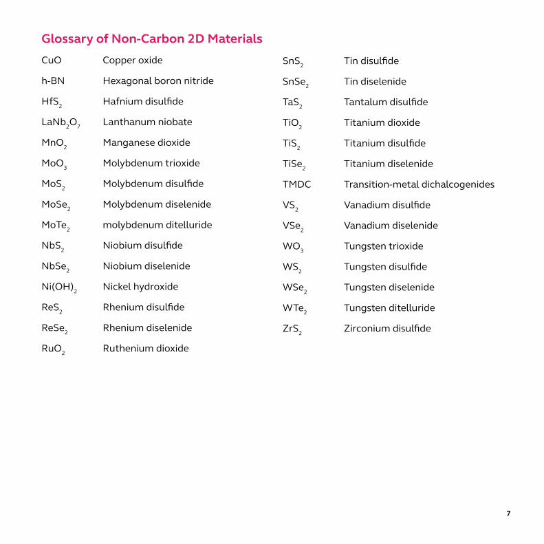
Glossary of Non-Carbon 2D Materials CuO Copper oxide
h-BN Hexagonal boron nitride
HfS2 Hafnium disulfide
LaNb2O7 Lanthanum niobate
MnO2 Manganese dioxide
MoO3 Molybdenum trioxide
MoS2 Molybdenum disulfide
MoSe2 Molybdenum diselenide
MoTe2 molybdenum ditelluride
NbS2 Niobium disulfide
NbSe2 Niobium diselenide
Ni(OH)2 Nickel hydroxide
ReS2 Rhenium disulfide
ReSe2 Rhenium diselenide
RuO2 Ruthenium dioxide
SnS2 Tin disulfide
SnSe2 Tin diselenide
TaS2 Tantalum disulfide
TiO2 Titanium dioxide
TiS2 Titanium disulfide
TiSe2 Titanium diselenide
TMDC Transition-metal dichalcogenides
VS2 Vanadium disulfide
VSe2 Vanadium diselenide
WO3 Tungsten trioxide
WS2 Tungsten disulfide
WSe2 Tungsten diselenide
WTe2 Tungsten ditelluride
ZrS2 Zirconium disulfide
8
1. IntroductionTwo-dimensional (2D) materials are a new and expanding family of materials with exceptional properties. Graphene is currently the most famous of these 2D materials, which although one million times thinner than paper is the strongest material known to science. It is made up of carbon atoms arranged in a hexagonal lattice and has many superlative properties to its credit. The unique combination of superior electrical, optical and mechanical properties makes graphene an incredible material for diverse applications across many sectors. The UK has been a global leader in research on graphene since its isolation from graphite crystal at the University of Manchester in 2004.
The ability to isolate or grow 2D materials has been a source of scientific fascination ever since it was shown to be possible. The isolation of graphene has led to the discovery of a whole family of 2D materials, including large numbers of atomic layers derived from non-carbon 2D materials such as hexagonal boron nitride (h-BN) and molybdenum disulphide (MoS2). These can be combined with graphene to create exciting new devices and products. This field is accelerating at a rapid pace and significant contributions have been made by UK researchers. This includes the
ability to build custom-made structures (hetero-structures) by stacking combinations of 2D materials on top of each other and constructing libraries of crystals to provide specific electrical, thermal, physical or mechanical properties and functionalities.
A number of these non-carbon 2D materials address graphene’s lack of band gap, which is what makes silicon and other semiconductors so useful for digital electronics. 2D semiconducting materials are likely to become an attractive choice for constructing digital circuits on flexible and transparent substrates for applications such as paper-like transparent displays, wearable electronics and photonic devices. In addition, the mechanical properties of MoS2 also appear to be very attractive. It is thought that there may be around five hundred 2D materials already developed, globally, including graphene.
Research in non-carbon 2D materials has benefited from the earlier investments in developing graphene with activities in areas of material structure-property correlations, synthesis and nanofabrication, device integration and device characterisation studies.
9
Many application sectors recognise the benefits they can derive from these new materials and have expressed the need to have greater understanding of the industrial challenges they will face. This led to the KTN undertaking a short project to bring together leading companies and academics working on 2D materials and devices from across the UK. The KTN also met with potential industry users and the wider supply chain to explore the challenges faced in bringing these 2D materials to market. The output from the project includes this state of the art report, which reviews the current innovation landscape. It captures the views of senior academics and the industrial community in terms of where the UK should be headed to create commercial value from developments in non-carbon 2D materials.
Definition of 2D Materials
An ISO terminology standard has been developed to provide a common definition of 2D materials. It defines 2D materials as “one or several layers with the atoms in each layer strongly bonded to neighbouring atoms in the same layer, which has one dimension, its thickness, in the nanoscale or smaller, and the other two dimensions generally at “larger scales”. See ISO/TS 80004-13:2017: ‘Graphene and related two-dimensional (2D) materials’.
10
11
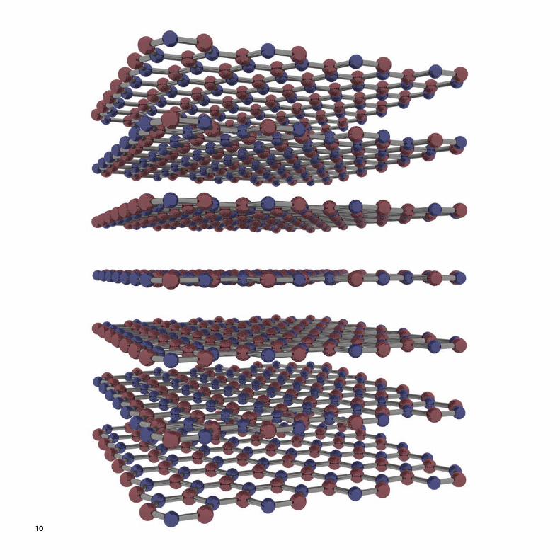
2. Family of Non-Carbon 2D MaterialsExperts claim that non-carbon 2D materials can pave the way to an exciting range of novel applications, particularly when used in combination with graphene. They base their views on the fact that these types of 2D materials can deliver high electrical and optical performance for applications such as photodetectors or digital electronics, due to the presence of band gap. This band gap property/function can be tuned through material processing, for instance, by changing the number of layers.
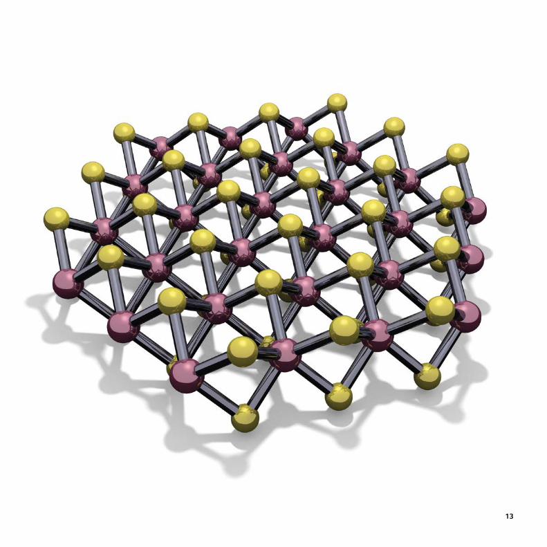
A summary of the most known and researched non-carbon 2D material families is shown in Table 1. One example is the 2D hexagonal Boron Nitride, h-BN, also called “white graphene”. This 2D material exhibits a natural band gap whilst providing good thermal conductivity. Another family of non-carbon 2D materials is the transition-metal dichalcogenides (TMDC) nanosheets. This family of layered materials, which include molybdenum disulphide (MoS2),
stabilises in a similar hexagonal structure and can exhibit a wide range of electronic properties ranging from semiconductor, metallic and even superconducting properties. These can be achieved by manipulating their composition, geometry, thickness and electronic density (Novoselov, 2016). Another family is 2D oxides such as layered CuO, MoO3 and WO3. These are known to exhibit a lower dielectric constant but larger band gaps than their 3D equivalents. Other 3D oxides have been reported to have been successfully exfoliated down to monolayers to create 2D structures, e.g. TiO2, MnO2, RuO2 and perovskite LaNb2O7. More recently, a new group of semiconductor 2D materials have been synthesised. These are made up of single elements such as silicene, phosphorene and germanene nanosheets. These materials tend to react with oxygen and thus are highly unstable in ambient conditions.
12
Table 1: Family of non-carbon 2D materials [(Novoselov, 2016), (Geim, 2013)]
Hexagonal boron nitride, h-BN • Large band gap in the UV range of the spectrum.• Resistant to mechanical and chemical interactions. • High dielectric strength. For instance, it can sustain electric fields up to Å0.8V/nm. • Application: substrate or encapsulation for 2D devices. For instance, combined with graphene,
h-BN greatly improves the mobility of graphene devices. Due to high dielectric strength, these have been characterised as gate dielectrics and tunnel barriers.
Transition-metal dichalcogenides, TMDCs• Compositions include WSe2, MoSe2, MoS2, MoTe2, WTe2, NbSe2, NbS2, TaS2.• Large optical absorption and band gap in the visible range of the spectrum.• Wide range of electronic properties can be obtained, from insulating, semiconducting to metallic
or semi-metallic. Properties can be tailored by changing composition, thickness, geometry and electronic density.
• Thin, transparent and flexible materials. • Applications include photovoltaic devices and photodetectors. For instance, a WS2 300 nm
film can absorb 95% of light. Moreover, semiconductor TMDCs with a direct gap like MoS2 are attractive for optics and optoelectronics devices.
2D oxides• Compositions include TiO2, MnO2, RuO2, perovskite LaNb2O7, hydroxide Ni(OH)2• Large band gap.• Low dielectric constant. • Biocompatible and non-toxic. • High surface to volume ratio and surface reactivity• High adsorption and catalytic efficiencies.• Applications include immobilisation of biomolecules, such as enzymes and antibodies.
Single element• Compositions include silicene, germanene and phosphorene. • Exhibit natural band gap.• Highly unstable (react with oxygen and water).• Grown on metallic substrates.• Mostly theoretical work.
13
14
15
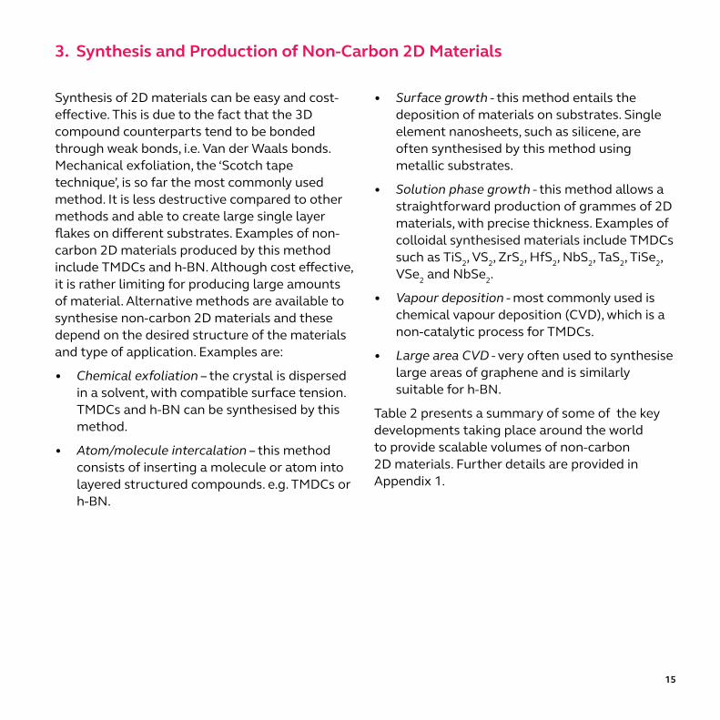
Synthesis of 2D materials can be easy and cost-effective. This is due to the fact that the 3D compound counterparts tend to be bonded through weak bonds, i.e. Van der Waals bonds. Mechanical exfoliation, the ‘Scotch tape technique’, is so far the most commonly used method. It is less destructive compared to other methods and able to create large single layer flakes on different substrates. Examples of non-carbon 2D materials produced by this method include TMDCs and h-BN. Although cost effective, it is rather limiting for producing large amounts of material. Alternative methods are available to synthesise non-carbon 2D materials and these depend on the desired structure of the materials and type of application. Examples are:
• Chemical exfoliation – the crystal is dispersed in a solvent, with compatible surface tension. TMDCs and h-BN can be synthesised by this method.
• Atom/molecule intercalation – this method consists of inserting a molecule or atom into layered structured compounds. e.g. TMDCs or h-BN.
• Surface growth - this method entails the deposition of materials on substrates. Single element nanosheets, such as silicene, are often synthesised by this method using metallic substrates.
• Solution phase growth - this method allows a straightforward production of grammes of 2D materials, with precise thickness. Examples of colloidal synthesised materials include TMDCs such as TiS2, VS2, ZrS2, HfS2, NbS2, TaS2, TiSe2, VSe2 and NbSe2.
• Vapour deposition - most commonly used is chemical vapour deposition (CVD), which is a non-catalytic process for TMDCs.
• Large area CVD - very often used to synthesise large areas of graphene and is similarly suitable for h-BN.
Table 2 presents a summary of some of the key developments taking place around the world to provide scalable volumes of non-carbon 2D materials. Further details are provided in Appendix 1.
3. Synthesis and Production of Non-Carbon 2D Materials
16
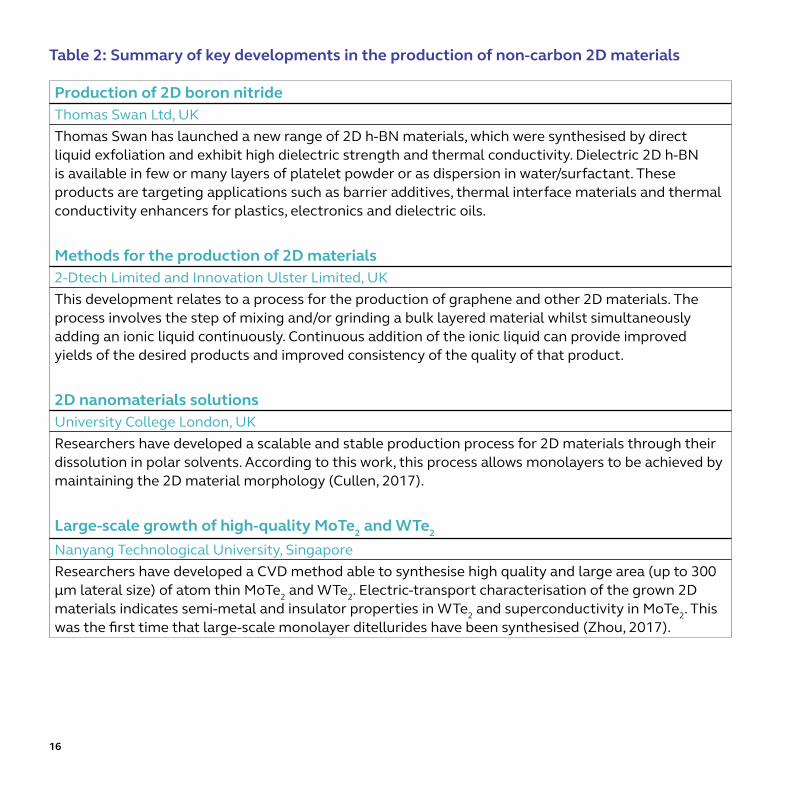
Table 2: Summary of key developments in the production of non-carbon 2D materials
Production of 2D boron nitrideThomas Swan Ltd, UKThomas Swan has launched a new range of 2D h-BN materials, which were synthesised by direct liquid exfoliation and exhibit high dielectric strength and thermal conductivity. Dielectric 2D h-BN is available in few or many layers of platelet powder or as dispersion in water/surfactant. These products are targeting applications such as barrier additives, thermal interface materials and thermal conductivity enhancers for plastics, electronics and dielectric oils.
Methods for the production of 2D materials2-Dtech Limited and Innovation Ulster Limited, UKThis development relates to a process for the production of graphene and other 2D materials. The process involves the step of mixing and/or grinding a bulk layered material whilst simultaneously adding an ionic liquid continuously. Continuous addition of the ionic liquid can provide improved yields of the desired products and improved consistency of the quality of that product.
2D nanomaterials solutionsUniversity College London, UKResearchers have developed a scalable and stable production process for 2D materials through their dissolution in polar solvents. According to this work, this process allows monolayers to be achieved by maintaining the 2D material morphology (Cullen, 2017).
Large-scale growth of high-quality MoTe2 and WTe2
Nanyang Technological University, SingaporeResearchers have developed a CVD method able to synthesise high quality and large area (up to 300 μm lateral size) of atom thin MoTe2 and WTe2. Electric-transport characterisation of the grown 2D materials indicates semi-metal and insulator properties in WTe2 and superconductivity in MoTe2. This was the first time that large-scale monolayer ditellurides have been synthesised (Zhou, 2017).
17
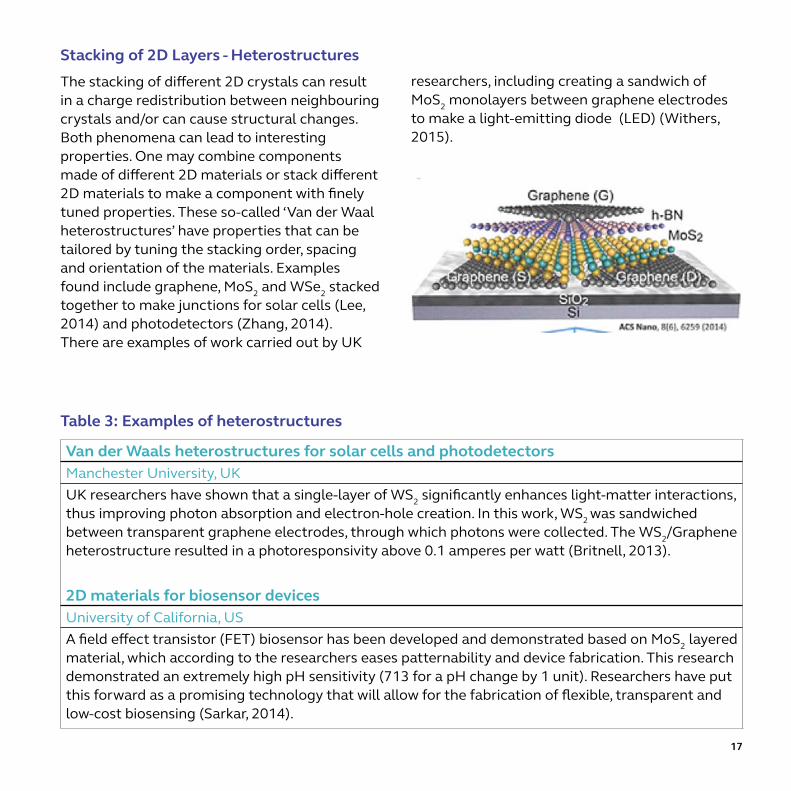
Stacking of 2D Layers - Heterostructures
The stacking of different 2D crystals can result in a charge redistribution between neighbouring crystals and/or can cause structural changes. Both phenomena can lead to interesting properties. One may combine components made of different 2D materials or stack different 2D materials to make a component with finely tuned properties. These so-called ‘Van der Waal heterostructures’ have properties that can be tailored by tuning the stacking order, spacing and orientation of the materials. Examples found include graphene, MoS2 and WSe2 stacked together to make junctions for solar cells (Lee, 2014) and photodetectors (Zhang, 2014). There are examples of work carried out by UK
researchers, including creating a sandwich of MoS2 monolayers between graphene electrodes to make a light-emitting diode (LED) (Withers, 2015).
Table 3: Examples of heterostructures
Van der Waals heterostructures for solar cells and photodetectors Manchester University, UKUK researchers have shown that a single-layer of WS2 significantly enhances light-matter interactions, thus improving photon absorption and electron-hole creation. In this work, WS2 was sandwiched between transparent graphene electrodes, through which photons were collected. The WS2/Graphene heterostructure resulted in a photoresponsivity above 0.1 amperes per watt (Britnell, 2013).
2D materials for biosensor devicesUniversity of California, USA field effect transistor (FET) biosensor has been developed and demonstrated based on MoS2 layered material, which according to the researchers eases patternability and device fabrication. This research demonstrated an extremely high pH sensitivity (713 for a pH change by 1 unit). Researchers have put this forward as a promising technology that will allow for the fabrication of flexible, transparent and low-cost biosensing (Sarkar, 2014).

18
19
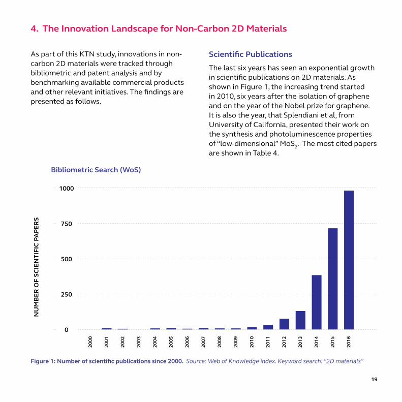
As part of this KTN study, innovations in non-carbon 2D materials were tracked through bibliometric and patent analysis and by benchmarking available commercial products and other relevant initiatives. The findings are presented as follows.
Scientific Publications
The last six years has seen an exponential growth in scientific publications on 2D materials. As shown in Figure 1, the increasing trend started in 2010, six years after the isolation of graphene and on the year of the Nobel prize for graphene. It is also the year, that Splendiani et al, from University of California, presented their work on the synthesis and photoluminescence properties of “low-dimensional” MoS2. The most cited papers are shown in Table 4.
Figure 1: Number of scientific publications since 2000. Source: Web of Knowledge index. Keyword search: “2D materials”
Bibliometric Search (WoS)
1000
YEAR
NU
MB
ER O
F SC
IEN
TIFI
C PA
PER
S
750
500
0
250
2000
2001
2002
2003
2004
2005
2006
2008
2009
2010
2011
2012
2013
2014
2015
2016
2007
4. The Innovation Landscape for Non-Carbon 2D Materials
20
21
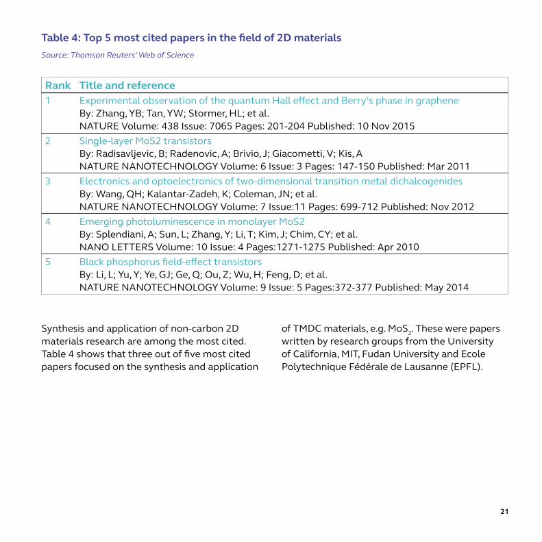
Rank Title and reference1 Experimental observation of the quantum Hall effect and Berry’s phase in graphene
By: Zhang, YB; Tan, YW; Stormer, HL; et al.NATURE Volume: 438 Issue: 7065 Pages: 201-204 Published: 10 Nov 2015
2 Single-layer MoS2 transistorsBy: Radisavljevic, B; Radenovic, A; Brivio, J; Giacometti, V; Kis, ANATURE NANOTECHNOLOGY Volume: 6 Issue: 3 Pages: 147-150 Published: Mar 2011
3 Electronics and optoelectronics of two-dimensional transition metal dichalcogenidesBy: Wang, QH; Kalantar-Zadeh, K; Coleman, JN; et al.NATURE NANOTECHNOLOGY Volume: 7 Issue:11 Pages: 699-712 Published: Nov 2012
4 Emerging photoluminescence in monolayer MoS2By: Splendiani, A; Sun, L; Zhang, Y; Li, T; Kim, J; Chim, CY; et al.NANO LETTERS Volume: 10 Issue: 4 Pages:1271-1275 Published: Apr 2010
5 Black phosphorus field-effect transistorsBy: Li, L; Yu, Y; Ye, GJ; Ge, Q; Ou, Z; Wu, H; Feng, D; et al.NATURE NANOTECHNOLOGY Volume: 9 Issue: 5 Pages:372-377 Published: May 2014
Synthesis and application of non-carbon 2D materials research are among the most cited. Table 4 shows that three out of five most cited papers focused on the synthesis and application
Table 4: Top 5 most cited papers in the field of 2D materials Source: Thomson Reuters’ Web of Science
of TMDC materials, e.g. MoS2. These were papers written by research groups from the University of California, MIT, Fudan University and Ecole Polytechnique Fédérale de Lausanne (EPFL).
22
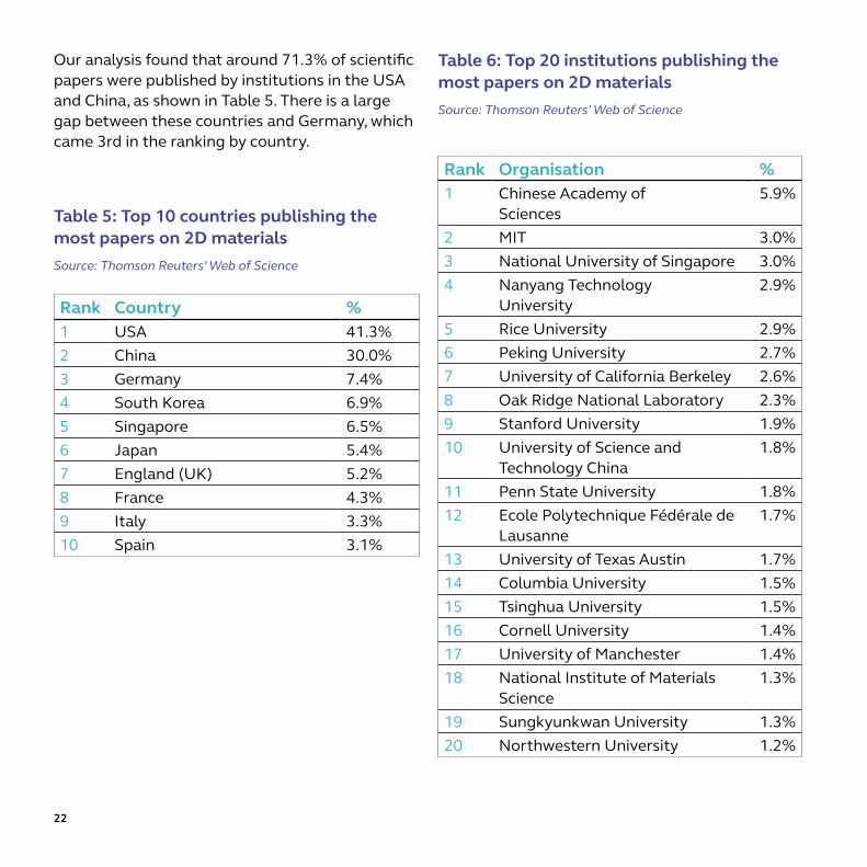
Our analysis found that around 71.3% of scientific papers were published by institutions in the USA and China, as shown in Table 5. There is a large gap between these countries and Germany, which came 3rd in the ranking by country.
Rank Country %1 USA 41.3%2 China 30.0%3 Germany 7.4%4 South Korea 6.9%5 Singapore 6.5%6 Japan 5.4%7 England (UK) 5.2%8 France 4.3%9 Italy 3.3%10 Spain 3.1%
Rank Organisation %1 Chinese Academy of
Sciences 5.9%
2 MIT 3.0%3 National University of Singapore 3.0%4 Nanyang Technology
University 2.9%
5 Rice University 2.9%6 Peking University 2.7%7 University of California Berkeley 2.6%8 Oak Ridge National Laboratory 2.3%9 Stanford University 1.9%10 University of Science and
Technology China1.8%
11 Penn State University 1.8%12 Ecole Polytechnique Fédérale de
Lausanne1.7%
13 University of Texas Austin 1.7%14 Columbia University 1.5%15 Tsinghua University 1.5%16 Cornell University 1.4%17 University of Manchester 1.4%18 National Institute of Materials
Science1.3%
19 Sungkyunkwan University 1.3%20 Northwestern University 1.2%
Table 5: Top 10 countries publishing the most papers on 2D materials Source: Thomson Reuters’ Web of Science
Table 6: Top 20 institutions publishing the most papers on 2D materials Source: Thomson Reuters’ Web of Science
23
The UK is ranked as the 7th country contributor to scientific publications on 2D materials. The University of Manchester leads this ranking in the UK, responsible for 1.4% of the UK’s 5.2% of scientific papers on non-carbon 2D materials produced worldwide. It is worth nothing that although the UK ranks 7th in this category, it has a world class reputation for the quality of its scientific understanding of 2D materials and provides leadership on many international collaborations.
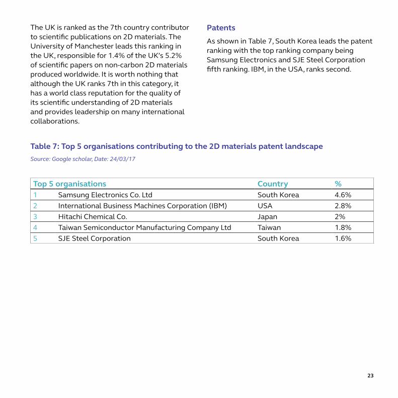
Patents
As shown in Table 7, South Korea leads the patent ranking with the top ranking company being Samsung Electronics and SJE Steel Corporation fifth ranking. IBM, in the USA, ranks second.
Top 5 organisations Country %1 Samsung Electronics Co. Ltd South Korea 4.6%2 International Business Machines Corporation (IBM) USA 2.8%3 Hitachi Chemical Co. Japan 2%4 Taiwan Semiconductor Manufacturing Company Ltd Taiwan 1.8%5 SJE Steel Corporation South Korea 1.6%
Table 7: Top 5 organisations contributing to the 2D materials patent landscapeSource: Google scholar, Date: 24/03/17
24
25
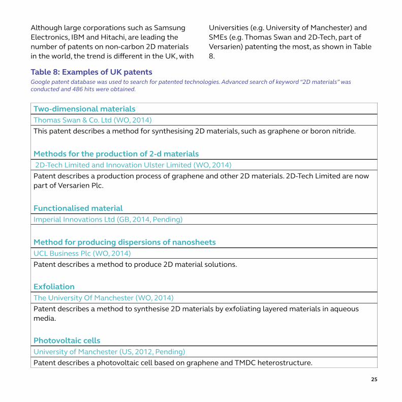
Although large corporations such as Samsung Electronics, IBM and Hitachi, are leading the number of patents on non-carbon 2D materials in the world, the trend is different in the UK, with
Two-dimensional materialsThomas Swan & Co. Ltd (WO, 2014)This patent describes a method for synthesising 2D materials, such as graphene or boron nitride.
Methods for the production of 2-d materials 2D-Tech Limited and Innovation Ulster Limited (WO, 2014)Patent describes a production process of graphene and other 2D materials. 2D-Tech Limited are now part of Versarien Plc.
Functionalised materialImperial Innovations Ltd (GB, 2014, Pending)
Method for producing dispersions of nanosheetsUCL Business Plc (WO, 2014)Patent describes a method to produce 2D material solutions.
ExfoliationThe University Of Manchester (WO, 2014)Patent describes a method to synthesise 2D materials by exfoliating layered materials in aqueous media.
Photovoltaic cellsUniversity of Manchester (US, 2012, Pending)Patent describes a photovoltaic cell based on graphene and TMDC heterostructure.
Table 8: Examples of UK patentsGoogle patent database was used to search for patented technologies. Advanced search of keyword “2D materials” was conducted and 486 hits were obtained.
Universities (e.g. University of Manchester) and SMEs (e.g. Thomas Swan and 2D-Tech, part of Versarien) patenting the most, as shown in Table 8.
26
27
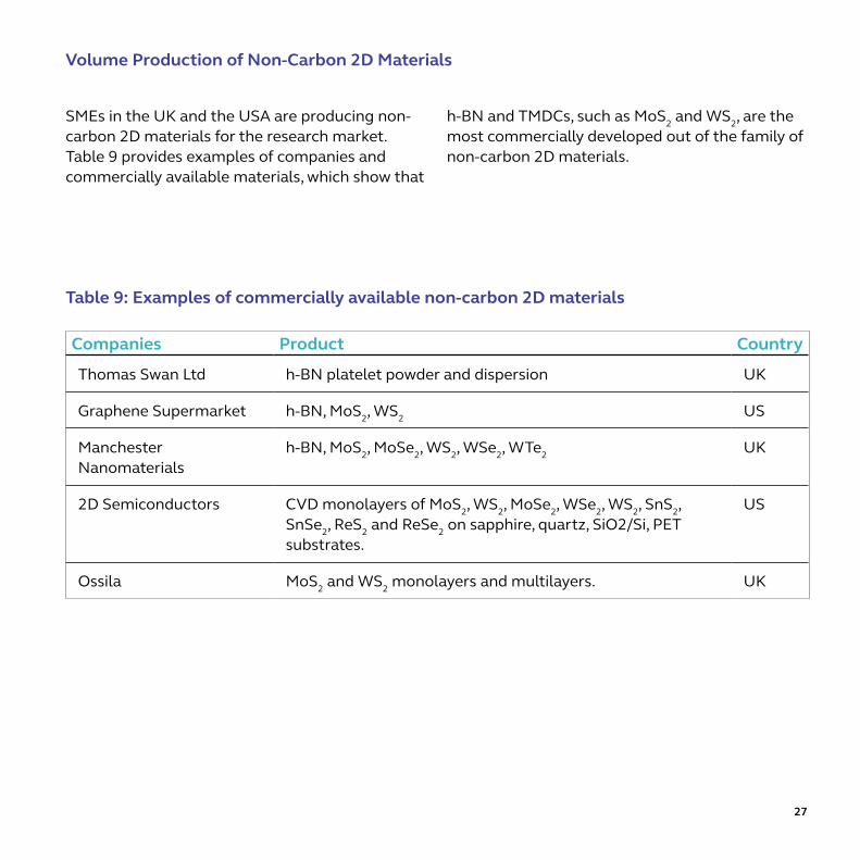
SMEs in the UK and the USA are producing non-carbon 2D materials for the research market. Table 9 provides examples of companies and commercially available materials, which show that
Companies Product Country
Thomas Swan Ltd h-BN platelet powder and dispersion UK
Graphene Supermarket h-BN, MoS2, WS2 US
Manchester Nanomaterials
h-BN, MoS2, MoSe2, WS2, WSe2, WTe2 UK
2D Semiconductors CVD monolayers of MoS2, WS2, MoSe2, WSe2, WS2, SnS2, SnSe2, ReS2 and ReSe2 on sapphire, quartz, SiO2/Si, PET substrates.
US
Ossila MoS2 and WS2 monolayers and multilayers. UK
Table 9: Examples of commercially available non-carbon 2D materials
h-BN and TMDCs, such as MoS2 and WS2, are the most commercially developed out of the family of non-carbon 2D materials.
Volume Production of Non-Carbon 2D Materials
28
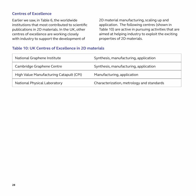
National Graphene Institute Synthesis, manufacturing, application
Cambridge Graphene Centre Synthesis, manufacturing, application
High Value Manufacturing Catapult (CPI) Manufacturing, application
National Physical Laboratory Characterization, metrology and standards
Centres of Excellence
Earlier we saw, in Table 6, the worldwide institutions that most contributed to scientific publications in 2D materials. In the UK, other centres of excellence are working closely with industry to support the development of
Table 10: UK Centres of Excellence in 2D materials
2D material manufacturing, scaling up and application. The following centres (shown in Table 10) are active in pursuing activities that are aimed at helping industry to exploit the exciting properties of 2D materials.
29
Technology roadmaps
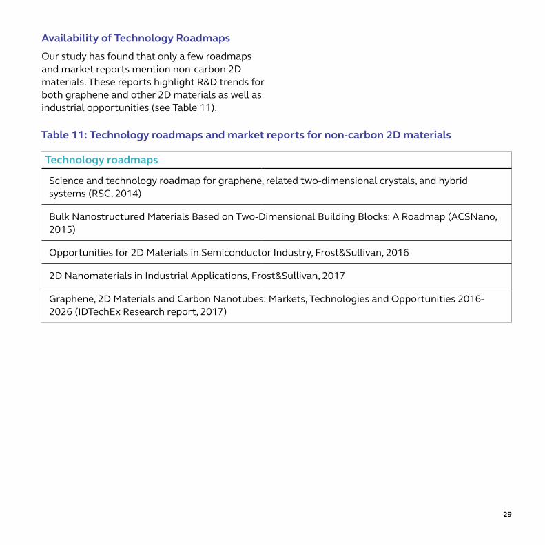
Science and technology roadmap for graphene, related two-dimensional crystals, and hybrid systems (RSC, 2014)
Bulk Nanostructured Materials Based on Two-Dimensional Building Blocks: A Roadmap (ACSNano, 2015)
Opportunities for 2D Materials in Semiconductor Industry, Frost&Sullivan, 2016
2D Nanomaterials in Industrial Applications, Frost&Sullivan, 2017
Graphene, 2D Materials and Carbon Nanotubes: Markets, Technologies and Opportunities 2016-2026 (IDTechEx Research report, 2017)
Availability of Technology Roadmaps
Our study has found that only a few roadmaps and market reports mention non-carbon 2D materials. These reports highlight R&D trends for both graphene and other 2D materials as well as industrial opportunities (see Table 11).
Table 11: Technology roadmaps and market reports for non-carbon 2D materials

30
31
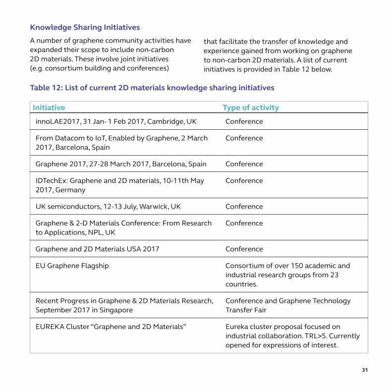
Knowledge Sharing Initiatives
A number of graphene community activities have expanded their scope to include non-carbon 2D materials. These involve joint initiatives (e.g. consortium building and conferences)
Initiative Type of activity
innoLAE2017, 31 Jan- 1 Feb 2017, Cambridge, UK Conference
From Datacom to IoT, Enabled by Graphene, 2 March 2017, Barcelona, Spain
Conference
Graphene 2017, 27-28 March 2017, Barcelona, Spain Conference
IDTechEx: Graphene and 2D materials, 10-11th May 2017, Germany
Conference
UK semiconductors, 12-13 July, Warwick, UK Conference
Graphene & 2-D Materials Conference: From Research to Applications, NPL, UK
Conference
Graphene and 2D Materials USA 2017 Conference
EU Graphene Flagship Consortium of over 150 academic and industrial research groups from 23 countries.
Recent Progress in Graphene & 2D Materials Research, September 2017 in Singapore
Conference and Graphene Technology Transfer Fair
EUREKA Cluster “Graphene and 2D Materials” Eureka cluster proposal focused on industrial collaboration. TRL>5. Currently opened for expressions of interest.
Table 12: List of current 2D materials knowledge sharing initiatives
that facilitate the transfer of knowledge and experience gained from working on graphene to non-carbon 2D materials. A list of current initiatives is provided in Table 12 below.

32
33
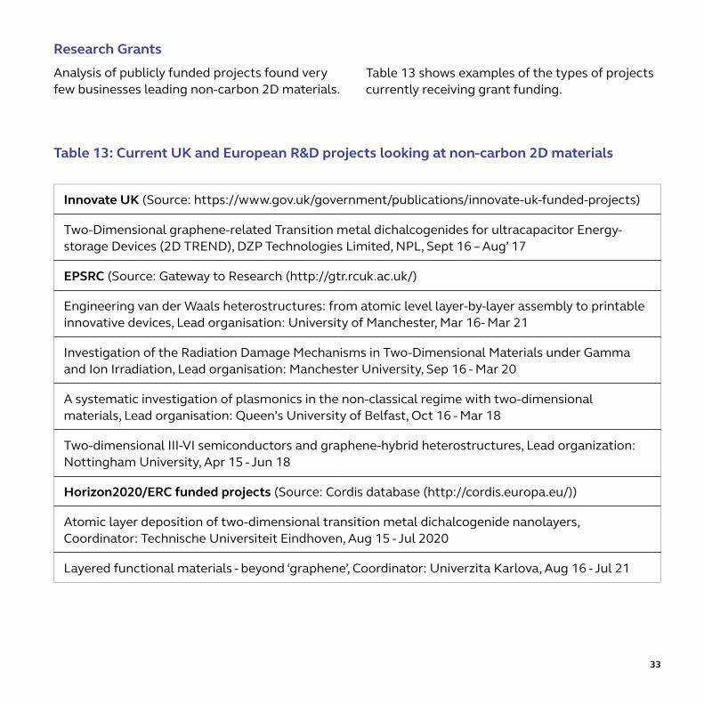
Research Grants
Analysis of publicly funded projects found very few businesses leading non-carbon 2D materials.
Innovate UK (Source: https://www.gov.uk/government/publications/innovate-uk-funded-projects)
Two-Dimensional graphene-related Transition metal dichalcogenides for ultracapacitor Energy-storage Devices (2D TREND), DZP Technologies Limited, NPL, Sept 16 – Aug’ 17
EPSRC (Source: Gateway to Research (http://gtr.rcuk.ac.uk/)
Engineering van der Waals heterostructures: from atomic level layer-by-layer assembly to printable innovative devices, Lead organisation: University of Manchester, Mar 16- Mar 21
Investigation of the Radiation Damage Mechanisms in Two-Dimensional Materials under Gamma and Ion Irradiation, Lead organisation: Manchester University, Sep 16 - Mar 20
A systematic investigation of plasmonics in the non-classical regime with two-dimensional materials, Lead organisation: Queen’s University of Belfast, Oct 16 - Mar 18
Two-dimensional III-VI semiconductors and graphene-hybrid heterostructures, Lead organization: Nottingham University, Apr 15 - Jun 18
Horizon2020/ERC funded projects (Source: Cordis database (http://cordis.europa.eu/))
Atomic layer deposition of two-dimensional transition metal dichalcogenide nanolayers, Coordinator: Technische Universiteit Eindhoven, Aug 15 - Jul 2020
Layered functional materials - beyond ‘graphene’, Coordinator: Univerzita Karlova, Aug 16 - Jul 21
Table 13: Current UK and European R&D projects looking at non-carbon 2D materials
Table 13 shows examples of the types of projects currently receiving grant funding.
34
Toxicity of Non-Carbon 2D Materials
There is ongoing research to assess the toxicological impact of non-carbon 2D materials. It is generally accepted by the scientific community that cytotoxicology of 2D materials is strongly affected not only by the chemical composition and defect density but also by parameters associated with the production process. For example, it has been found that the in-vitro cytotoxicity of exfoliated MoS2 nanosheet depends on the intercalating agent used for the exfoliation; the more layers that are exfoliated the stronger the impact of toxicity. This has been associated with the increase of surface area and the number of active edge sites (Chang, 2014).

35
5. Strategic Insights for the UKTo make sense of the trends in the innovation landscape of non-carbon 2D materials and how these should shape the UK’s industrial approach to this family of 2D materials, KTN consulted with
industry and academia to look at opportunities and challenges. Table 14 sums up a wide range of potential applications with significant export opportunities for the UK.
36
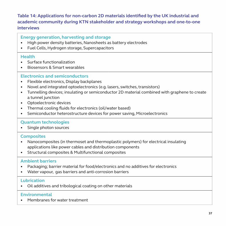
37
Energy generation, harvesting and storage• High power density batteries, Nanosheets as battery electrodes• Fuel Cells, Hydrogen storage, Supercapacitors
Health • Surface functionalization• Biosensors & Smart wearables
Electronics and semiconductors • Flexible electronics, Display backplanes• Novel and integrated optoelectronics (e.g. lasers, switches, transistors) • Tunnelling devices; insulating or semiconductor 2D material combined with graphene to create
a tunnel junction• Optoelectronic devices• Thermal cooling fluids for electronics (oil/water based)• Semiconductor heterostructure devices for power saving, Microelectronics
Quantum technologies• Single photon sources
Composites• Nanocomposites (in thermoset and thermoplastic polymers) for electrical insulating
applications like power cables and distribution components • Structural composites & Multifunctional composites
Ambient barriers• Packaging; barrier material for food/electronics and no additives for electronics• Water vapour, gas barriers and anti-corrosion barriers
Lubrication • Oil additives and tribological coating on other materials
Environmental• Membranes for water treatment
Table 14: Applications for non-carbon 2D materials identified by the UK industrial and academic community during KTN stakeholder and strategy workshops and one-to-one interviews
38
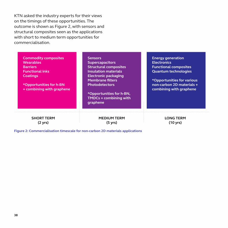
KTN asked the industry experts for their views on the timings of these opportunities. The outcome is shown as Figure 2, with sensors and structural composites seen as the applications with short to medium term opportunities for commercialisation.
SHORT TERM(2 yrs)
MEDIUM TERM(5 yrs)
LONG TERM(10 yrs)
Commodity compositesWearablesBarriersFunctional inksCoatings
*Opportunities for h-BN+ combining with graphene
SensorsSupercapacitorsStructural compositesInsulation materialsElectronic packagingMembrane filtersPhotodetectors
*Opportunities for h-BN, TMDCs + combining with graphene
Energy generationElectronicsFunctional compositesQuantum technologies
*Opportunities for various non-carbon 2D materials +combining with graphene
Figure 2: Commercialisation timescale for non-carbon 2D materials applications
39
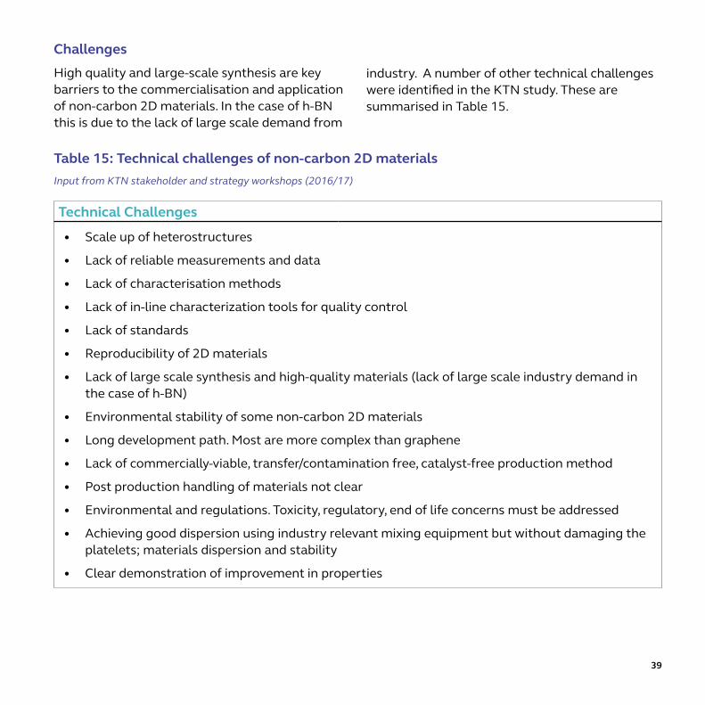
Challenges
High quality and large-scale synthesis are key barriers to the commercialisation and application of non-carbon 2D materials. In the case of h-BN this is due to the lack of large scale demand from
Technical Challenges
• Scale up of heterostructures
• Lack of reliable measurements and data
• Lack of characterisation methods
• Lack of in-line characterization tools for quality control
• Lack of standards
• Reproducibility of 2D materials
• Lack of large scale synthesis and high-quality materials (lack of large scale industry demand in the case of h-BN)
• Environmental stability of some non-carbon 2D materials
• Long development path. Most are more complex than graphene
• Lack of commercially-viable, transfer/contamination free, catalyst-free production method
• Post production handling of materials not clear
• Environmental and regulations. Toxicity, regulatory, end of life concerns must be addressed
• Achieving good dispersion using industry relevant mixing equipment but without damaging the platelets; materials dispersion and stability
• Clear demonstration of improvement in properties
Table 15: Technical challenges of non-carbon 2D materials Input from KTN stakeholder and strategy workshops (2016/17)
industry. A number of other technical challenges were identified in the KTN study. These are summarised in Table 15.
40
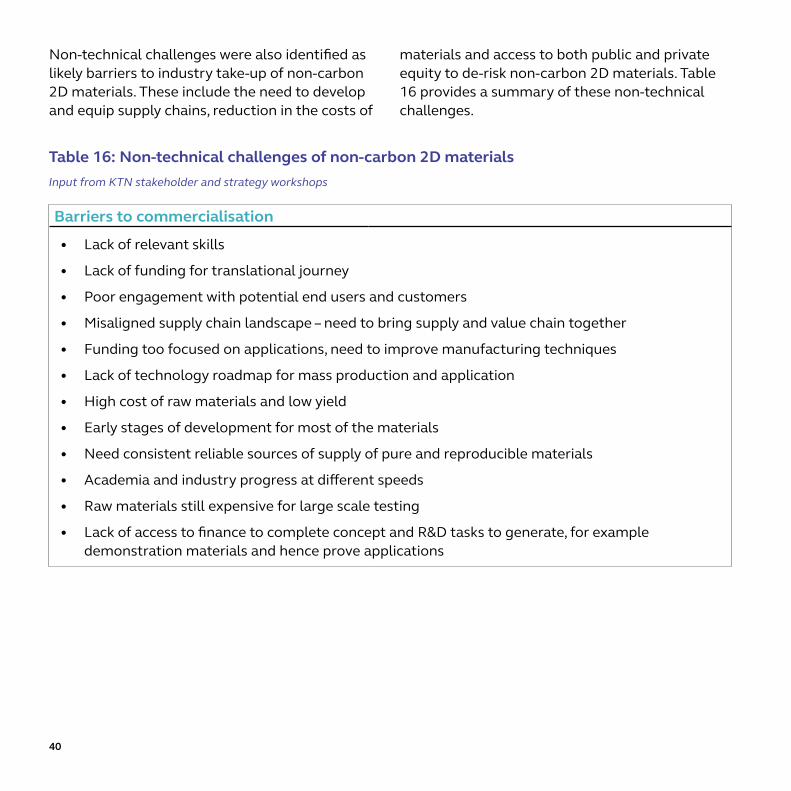
Non-technical challenges were also identified as likely barriers to industry take-up of non-carbon 2D materials. These include the need to develop and equip supply chains, reduction in the costs of
materials and access to both public and private equity to de-risk non-carbon 2D materials. Table 16 provides a summary of these non-technical challenges.
Barriers to commercialisation
• Lack of relevant skills
• Lack of funding for translational journey
• Poor engagement with potential end users and customers
• Misaligned supply chain landscape – need to bring supply and value chain together
• Funding too focused on applications, need to improve manufacturing techniques
• Lack of technology roadmap for mass production and application
• High cost of raw materials and low yield
• Early stages of development for most of the materials
• Need consistent reliable sources of supply of pure and reproducible materials
• Academia and industry progress at different speeds
• Raw materials still expensive for large scale testing
• Lack of access to finance to complete concept and R&D tasks to generate, for example demonstration materials and hence prove applications
Table 16: Non-technical challenges of non-carbon 2D materials Input from KTN stakeholder and strategy workshops
41
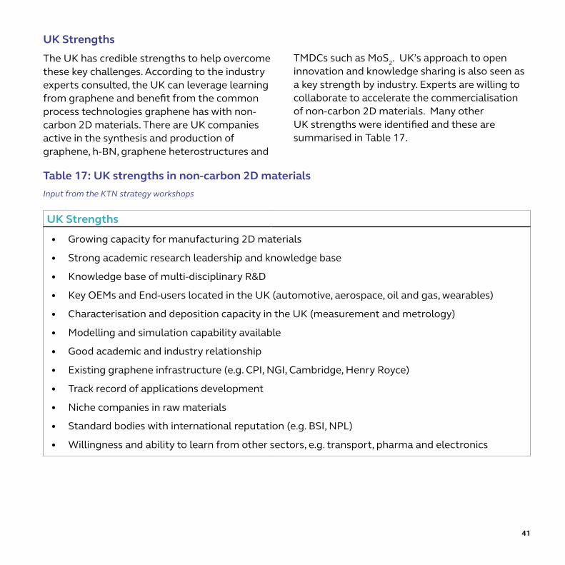
UK Strengths
• Growing capacity for manufacturing 2D materials
• Strong academic research leadership and knowledge base
• Knowledge base of multi-disciplinary R&D
• Key OEMs and End-users located in the UK (automotive, aerospace, oil and gas, wearables)
• Characterisation and deposition capacity in the UK (measurement and metrology)
• Modelling and simulation capability available
• Good academic and industry relationship
• Existing graphene infrastructure (e.g. CPI, NGI, Cambridge, Henry Royce)
• Track record of applications development
• Niche companies in raw materials
• Standard bodies with international reputation (e.g. BSI, NPL)
• Willingness and ability to learn from other sectors, e.g. transport, pharma and electronics
UK Strengths
The UK has credible strengths to help overcome these key challenges. According to the industry experts consulted, the UK can leverage learning from graphene and benefit from the common process technologies graphene has with non-carbon 2D materials. There are UK companies active in the synthesis and production of graphene, h-BN, graphene heterostructures and
TMDCs such as MoS2. UK’s approach to open innovation and knowledge sharing is also seen as a key strength by industry. Experts are willing to collaborate to accelerate the commercialisation of non-carbon 2D materials. Many other UK strengths were identified and these are summarised in Table 17.
Table 17: UK strengths in non-carbon 2D materials Input from the KTN strategy workshops
42
6. Conclusions This KTN study has identified a body of work being undertaken globally to develop non-carbon 2D materials, mainly led by university research groups. Companies such as Samsung and IBM are active in this area and so are UK SMEs such as Thomas Swan and 2D-Tech, part of Versarien Plc. The discussions KTN has had with UK companies suggest that existing businesses developing graphene are the ones most likely to look at exploiting other 2D materials.
Clear progress has been made with the commercial availability of hexagonal Boron Nitride, h-BN. There is a growing industry interest in transition-metal dichalcogenides (TMDCs), in particular semiconductor TMDCs such as MoS2, which have direct band gap and are attractive for optics and optoelectronic devices.
There is also a particular excitement about the ability to custom stack thin layers of non-carbon 2D materials and, in combination with graphene, create hetero-structured devices. These devices have a variety of different electronic and optical properties, which can be finely tuned by careful design of the stack. Ongoing research is showing great promise for new materials with specially designed electrical, magnetic, piezoelectric and optical functionalities.
43
7. Priorities and RecommendationsThe industry experts who engaged with the KTN at the stakeholder and strategy workshops saw the following as priorities for the UK:
• More industry collaboration needed to scale up the manufacturing and use of 2D materials;
• UK industry to work closely with academic researchers to develop technology roadmaps for mass production and application of 2D materials;
• Funding needed to improve manufacturing techniques for 2D materials, including device fabrication and product manufacture.
Following considerable discussions with the industry experts and academics, the following recommendations are made to both government and industry to drive forward the commercialisation of non-carbon 2D materials in the UK:
1. Create an Industry Challenge around h-BN and TMDCs to accelerate the development of supply chain and end user partnerships.
2. Provide 5-10 years long term funding for centres of excellence to carry out more work needed in scale-up of non-carbon 2D material production, device fabrication and end-user applications.
3. Invest in scaled-up demonstrators to show and exploit the game changing properties of non-carbon 2D materials, solely or in combination with graphene.
4. Consider the overall UK landscape and impact of the EU Graphene Flagship project on leveraged funding for development and commercialisation activities.

44
AcknowledgementsKTN would like to express sincere thanks to the many individual experts and organisations that have contributed to this review and analysis. In particular, we would like to thank the many contributors who attended the stakeholder and strategy workshops and also those who spoke to us during visits and completed the online questionnaire.
45
References Britnell L. , R. M. Ribeiro, A. Eckmann, R. Jalil, B. D. Belle, A. Mishchenko, Y.-J. Kim, R. V. Gorbachev, T. Georgiou, S. V. Morozov, A. N. Grigorenko, A. K. Geim, C. Casiraghi, A. H. Castro Neto, K. S. Novoselov, Strong Light-Matter Interactions in Heterostructures of Atomically Thin Films, SCIENCE VOL 3, 1311-1314 (2013)
Chang E. L. K., Soferb Z., Pumer M., MoS2 exhibits stronger toxicity with increased exfoliation, Nanoscale,6(23),14412-8 (2014)
Cullen P., Cox K. M., Subhan M. K. B., Picco L., Payton O.D., Buckley D. J., Miller T. S., Hodge S. A., Skipper N. T., Tileli V., Howard C., Ionic solutions of two-dimensional materials, Nature Chemistry 9, 244–249 (2017)
Sarkar D., Liu W., Xie X., Anselmo A. C., Mitragotri S., Banerjee K., MoS2 Field-Effect Transistor for Next-Generation Label-Free Biosensors, ACS Nano, 8 (4), 3992–4003 (2014)
Zhou J., Liu F., Huang X., Xia J., Zhang B., Zeng Q., Wang H., Zhu C., Niu L., Wang X., Fu W., Yu P., Chang T. R., Hsu C. H., Wu D., Jeng H. T., Huang Y., Lin H., Shen Z., Yang C., Lu L., Suenaga K., Zhou W., Pantelides S. T., Liu G., Liu Z., Large-area and high-quality 2D transition metal telluride, Adv. Mater. 29, 1603471 (2017)
Kalantar-zadeh K., Ou J. Z., Daeneke T., Strano M. S., Pumera M., Gras S. L., Two-Dimensional Transition Metal Dichalcogenides in Biosystems, Advanced Functional Materials, 25, Issue 32, 5086–5099 (2015)
ISO terminology standard – ISO/TS 80004-13:2017: ‘Graphene and related two-dimensional (2D) materials’
2D Nanomaterials in Industrial Applications. TechVision Opportunity Engines. Retrieved from Frost & Sullivan database. (2017). [No authors listed]
Opportunities for 2D Materials in Semiconductor Industry (TechVision). TechVision Analysis. Retrieved from Frost & Sullivan database (2016). [No authors listed]
“2D Boron Nitride Products”, 2016. Retrieved from: http://www.thomas-swan.co.uk/sites/pdf/Boron_Nitride_Products_FINAL_March2016.pdf
46
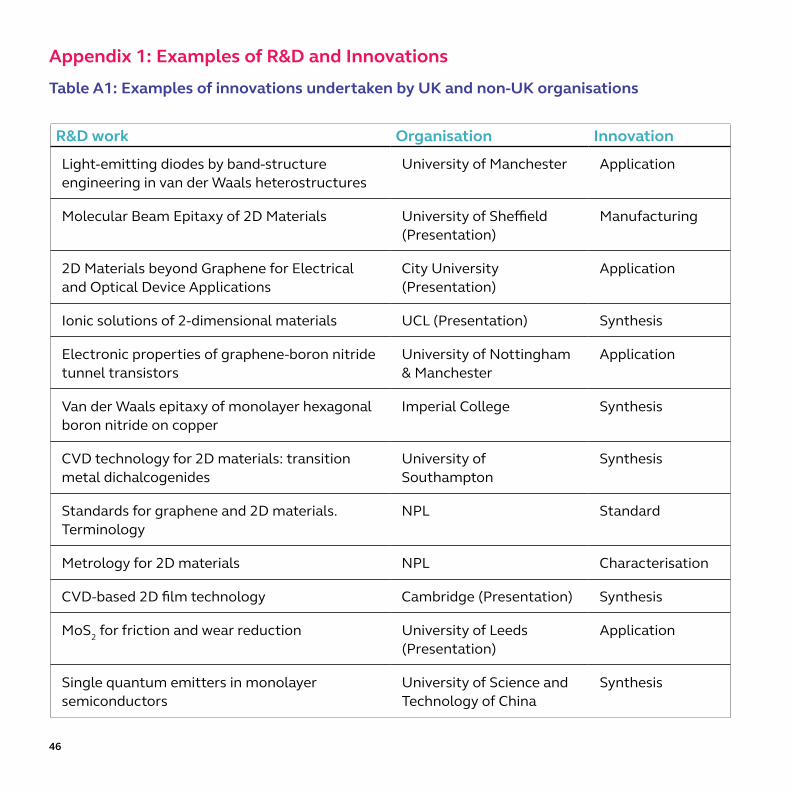
R&D work Organisation Innovation
Light-emitting diodes by band-structure engineering in van der Waals heterostructures
University of Manchester Application
Molecular Beam Epitaxy of 2D Materials University of Sheffield (Presentation)
Manufacturing
2D Materials beyond Graphene for Electrical and Optical Device Applications
City University (Presentation)
Application
Ionic solutions of 2-dimensional materials UCL (Presentation) Synthesis
Electronic properties of graphene-boron nitride tunnel transistors
University of Nottingham & Manchester
Application
Van der Waals epitaxy of monolayer hexagonal boron nitride on copper
Imperial College Synthesis
CVD technology for 2D materials: transition metal dichalcogenides
University of Southampton
Synthesis
Standards for graphene and 2D materials. Terminology
NPL Standard
Metrology for 2D materials NPL Characterisation
CVD-based 2D film technology Cambridge (Presentation) Synthesis
MoS2 for friction and wear reduction University of Leeds (Presentation)
Application
Single quantum emitters in monolayer semiconductors
University of Science and Technology of China
Synthesis
Appendix 1: Examples of R&D and Innovations
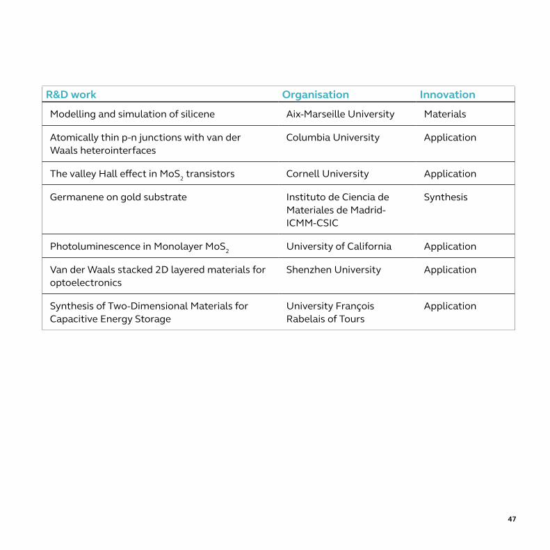
Table A1: Examples of innovations undertaken by UK and non-UK organisations
47
R&D work Organisation Innovation
Modelling and simulation of silicene Aix-Marseille University Materials
Atomically thin p-n junctions with van der Waals heterointerfaces
Columbia University Application
The valley Hall effect in MoS2 transistors Cornell University Application
Germanene on gold substrate Instituto de Ciencia de Materiales de Madrid-ICMM-CSIC
Synthesis
Photoluminescence in Monolayer MoS2 University of California Application
Van der Waals stacked 2D layered materials for optoelectronics
Shenzhen University Application
Synthesis of Two-Dimensional Materials for Capacitive Energy Storage
University François Rabelais of Tours
Application
48
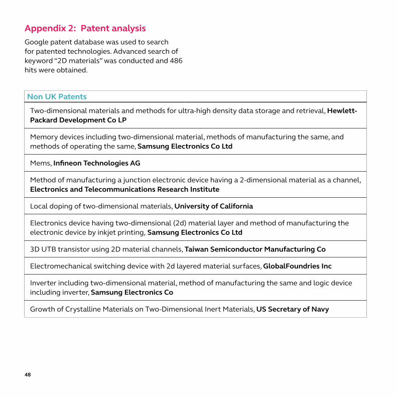
Appendix 2: Patent analysisGoogle patent database was used to search for patented technologies. Advanced search of keyword “2D materials” was conducted and 486 hits were obtained.
Non UK Patents
Two-dimensional materials and methods for ultra-high density data storage and retrieval, Hewlett-Packard Development Co LP
Memory devices including two-dimensional material, methods of manufacturing the same, and methods of operating the same, Samsung Electronics Co Ltd
Mems, Infineon Technologies AG
Method of manufacturing a junction electronic device having a 2-dimensional material as a channel, Electronics and Telecommunications Research Institute
Local doping of two-dimensional materials, University of California
Electronics device having two-dimensional (2d) material layer and method of manufacturing the electronic device by inkjet printing, Samsung Electronics Co Ltd
3D UTB transistor using 2D material channels, Taiwan Semiconductor Manufacturing Co
Electromechanical switching device with 2d layered material surfaces, GlobalFoundries Inc
Inverter including two-dimensional material, method of manufacturing the same and logic device including inverter, Samsung Electronics Co
Growth of Crystalline Materials on Two-Dimensional Inert Materials, US Secretary of Navy

49
Notes

Notes

Head Office
Knowledge Transfer Network Ltd
Suite 218 Business Design Centre
52 Upper Street
Islington
London N1 0QH
Telephone: 03333 403251
Email: [email protected]
ktn-uk.org
@KTNUK


