
CHAPTER 7
Flip-Flops, Registers, Counters, and a Simple Processor

Chapter Objectives
In this chapter you will learn about: Logic circuits that can store information Flip-flops, which store a single bit Registers, which store multiple bits Shift registers, which shift the contents of a
register Counters of various types VHDL constructs used to implement storage
elements Design of small subsystems Timing considerations

Memoryelement Alarm
Sensor
Reset
Set
On Off
Motivation: Control of an Alarm System
Alarm turned on when On/Off = 1 Alarm turned off when On/Off = 0 Once triggered, alarm stays on until
manually reset The circuit requires a memory element

The Basic Latch
Basic latch is a feedback connection of two NOR gates or two NAND gates
It can store one bit of information It can be set to 1 using the S input and
reset to 0 using the R input.

A B
A Simple Memory Element
A feedback loop with even number of inverters
If A = 0, B = 1 or when A = 1, B = 0 This circuit is not useful due to the lack
of a mechanism for changing its state

Reset
Set Q
A Memory Element with NOR Gates

The Gated Latch
Gated latch is a basic latch that includes input gating and a control signal
The latch retains its existing state when the control input is equal to 0
Its state may be changed when the control signal is equal to 1. In our discussion we referred to the control input as the clock
We consider two types of gated latches: Gated SR latch uses the S and R inputs to set the latch
to 1 or reset it to 0, respectively. Gated D latch uses the D input to force the latch into a
state that has the same logic value as the D input.

Gated S/R Latch

Gated D Latch

t su
t h
Clk
D
Q
Setup and Hold Times
Setup Time tsu
The minimum time that the input signal must be stable prior to the edge of the clock signal.
Hold Time th
The minimum time that the input signal must be stable after the edge of the clock signal.

Flip-Flops
A flip-flop is a storage element based on the gated latch principle
It can have its output state changed only on the edge of the controlling clock signal

Flip-Flops
We consider two types: Edge-triggered flip-flop is affected only by
the input values present when the active edge of the clock occurs
Master-slave flip-flop is built with two gated latches The master stage is active during half of the clock
cycle, and the slave stage is active during the other half.
The output value of the flip-flop changes on the edge of the clock that activates the transfer into the slave stage.

D Q
Q
Master Slave
D
Clock
Q
Q
D Q
Q
Q m Q s
D
Clock
Q m
Q Q s =
D Q
Q
(a) Circuit
(b) Timing diagram
(c) Graphical symbol
Clk Clk
Master-Slave D Flip-Flop

D Q
Q
Graphical symbol
Clock
A Positive-Edge-Triggered D Flip-Flop

Comparison of Level-Sensitive and Edge-Triggered D Storage Elements

D Q
Q
Clear
Preset
Master-Slave D Flip-Flop with Clear and Preset

T Flip-Flop
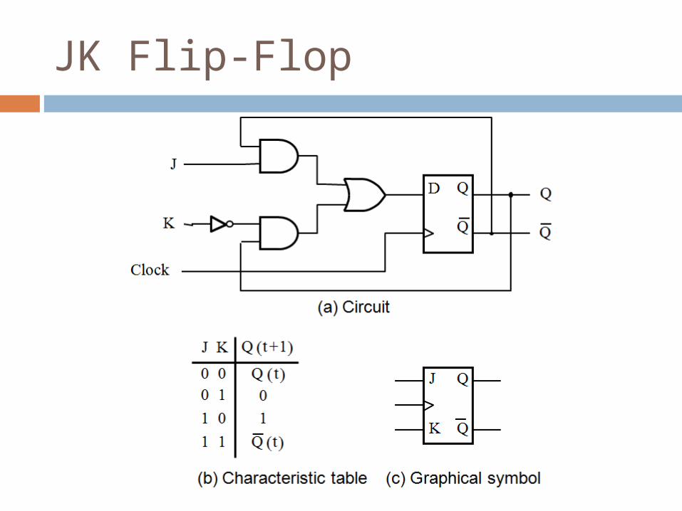
JK Flip-Flop

Registers and Counters
An n-bit register is a cascade of n flip-flops and can store an n-bit binary data
A counter can count occurrences of events and can generate timing intervals for control purposes

A Simple Shift Register

Parallel-Access Shift Register
Performs both as a series-to-parallel and a parallel-to-series converter

A Three-Bit Up-Counter
Q1 is connected to clk, Q2 and Q3 are clocked by Q’ of the preceding stage (hence called asynchronous or ripple counter)

A Three-Bit Down-Counter
Q1 is connected to clk, Q2 and Q3 are clocked by Q of the preceding stage (asynchronous or ripple counter)

0 0 1 1
0 1 0 1
0 1 2 3
0 0 1
0 1 0
4 5 6
1 1 7
0 0 0 0 1 1 1 1
Clock cycle
0 0 8 0
Q 2 Q1 Q0 Q 1 changes
Q 2 changes
Derivation of the Synchronous Up-Counter Q0 changes with clk, Q2 changes when previous state of Q0
was 1, and Q3 changes when previous state of Q1 and Q0 were 1

A Four-Bit Synchronous Up-Counter

T Q
Q Clock
T Q
Q
Enable
Clear
T Q
Q
T Q
Q
Inclusion of Enable and Clear Capability


