
NANOYOU Teachers Training Kit in Nanoscience and Nanotechnologies
Chapter 6 –
Characterisation
Methods Module 1- Fundamental concepts in nanoscience and nanotechnologies
Written by Luisa Filipponi and Duncan Sutherland
Interdisciplinary Nanoscience Centre (iNANO)
Aarhus University, Denmark
January 2010
Creative Commons Attribution ShareAlike 3.0 unless indicated in text or figure captions.
This document has been created in the context of the NANOYOU project (WP4). All information is provided “as is”
and no guarantee or warranty is given that the information is fit for any particular purpose. The user thereof uses
the information at its sole risk and liability. The document reflects solely the views of its authors. The European
Commission is not liable for any use that may be made of the information contained therein.
NANOYOU Teachers Training Kit – Module 1– Chapter 6
Page 2 of 13
The research leading to these results has received funding from the European Community's Seventh Framework Programme
(FP7/2007-2013) under grant agreement n° 233433
Contents
Microscopy ............................................................................................................................................ 3
Scanning tunnelling microscope ...................................................................................................................................... 5
Operational principle of the STM ................................................................................................................................ 5
How are images created? ............................................................................................................................................ 7
Atomic Force Microscope ................................................................................................................................................. 9
Spectroscopy methods ........................................................................................................................ 11
X-ray methods ................................................................................................................................................................. 11
UV-Visible plasmon absorption and emission .............................................................................................................. 12
Plasmon resonance light scattering .............................................................................................................................. 12
Surface-Enhanced Raman Scattering ............................................................................................................................ 13
Non-radiative and non-electron characterisation methods ............................................................ 13
NANOYOU Teachers Training Kit – Module 1– Chapter 6
Page 3 of 13
The research leading to these results has received funding from the European Community's Seventh Framework Programme
(FP7/2007-2013) under grant agreement n° 233433
Chapter 6: Characterisation methods
“Seeing is believing.” Therefore imaging of nanomaterials is an essential part of nanoscience and
nanotechnologies. Imaging in nanoscience does not just mean “to create an image”, but to understand
its meaning. Scientists nowadays have access to a variety of truly amazing instruments that allow them
to see objects at the nanoscale. This was a dream for scientists until just a couple of decades ago, a
dream that came true in the mid 1980s when a revolutionary instrument was invented, the Scanning
Tunnelling Microscope, and shortly after, the Atomic Force Microscope. As a matter of fact it was the
invention of those instruments that truly opened the doors to the nanoworld. Once scientists were able
to see nanoscale objects, they started to be able to analyse them, understand their behaviour, and
imagine ways of manipulating them.
This chapter summarises some of the methods that are used for the imaging and characterisation of
nanomaterials, meaning materials with at least one dimension in the nanoscale regime (1-100nm).
These include nanostructured surfaces, nanoparticles, nanoporous materials, etc. The aim of this
chapter is to answer the questions: how do we image and characterise nanomaterials?
There are many methods to image nanostructured materials (e.g. a nanostructured surface) and to
characterise their physical and chemical properties. Here we provide only a short review and description
of these methods, but the interested teacher can find more resources at the end of the chapter.
In general two fundamental types of characterisation methods exist: imaging by microscopy and analysis
by spectroscopy. The methods employed have been developed specifically to meet the characterisation
needs of nanomaterials.
Microscopy
An optical microscope uses visible light (i.e. an electromagnetic radiation) and a system of lenses to
magnify images of small samples. For this reason it is also called a light microscope. Optical microscopes
are the oldest and simplest of the microscopes. The resolution limit of an optical microscope is imposed
NANOYOU Teachers Training Kit – Module 1– Chapter 6
Page 4 of 13
The research leading to these results has received funding from the European Community's Seventh Framework Programme
(FP7/2007-2013) under grant agreement n° 233433
by the wavelength of the visible light.1 Visible light has wavelengths between 400 and 700 nm. The
resolving power of an optical microscope is around 0.2 µm or 200 nm. Thus for two objects to be
distinguishable, they need to be separated by at least 200 nm. Single objects smaller than this limit are
not distinguishable; they are seen as “fuzzy objects”. This is known as the “diffraction limit” of visible
light.
In order to overcome the limitations set by the diffraction limit of visible light other microscopes have
been designed which use other beams: rather than light they use electron beams to illuminate the
sample. Electron microscopes have much greater resolving power than light microscopes that use
electromagnetic radiation and can obtain much higher magnifications of up to 2 million times, while the
best light microscopes are limited to magnifications of 2000 times. Both electron and light microscopes
have resolution limitations, imposed by the wavelength of the radiation they use. The greater resolution
and magnification of the electron microscope is because the wavelength of an electron (its de Broglie
wavelength) is much smaller than that of a photon of visible light.
There are various types of electron microscopes, such as the scanning electron microscope (SEM), or
the transmission electron microscope (TEM). Conceptually, these microscopes are similar to an optical
microscope in the sense that they use a radiation to visualise a sample: photons in the case of an optical
microscope, and electrons (i.e. particles) in the case of electron microscopes.
In 1981, a totally new concept of imaging was introduced by Binning and his co-workers from IBM. They
used a small metal tip placed at a minute distance from a conducting surface: when the two are placed
very close together, but not actually touching, a bias between the two can allow electrons to tunnel
through the vacuum between them. This creates a tunnelling current,2 which can be measured and
which is a function of the electron density on the surface. Electron density is the probability of finding an
electron in a particular place. There is high electron density around the atoms and bonds in molecules.
This type of microscope is called the scanning tunnelling microscope (STM). Variations in current as the
probe passes over the surface are translated into an image. The STM can create detailed 3D images of a
1 As a general rule of thumb, the resolution is about half the wavelength used in the measurement.
2 For a definition and description of the tunnelling effect see Chapter 4.
NANOYOU Teachers Training Kit – Module 1– Chapter 6
Page 5 of 13
The research leading to these results has received funding from the European Community's Seventh Framework Programme
(FP7/2007-2013) under grant agreement n° 233433
Figure 2. (Left) A 3 mm tip
positioned 0.1 nm above the
surface. (Right) Macroscopic
analogy: a 300 m high Eiffel
Tower located 0.01 mm
above the city.
sample with atomic resolution. This means that the resolution is actually so high that it is possible to see
and distinguish the individual atoms (0.2 nm = 2 * 10-10 m) on the surface. The invention of the STM
earned Binning and his co-worker Heinrich Rohrer (at IBM Zürich) the Nobel Prize in Physics in 1986.
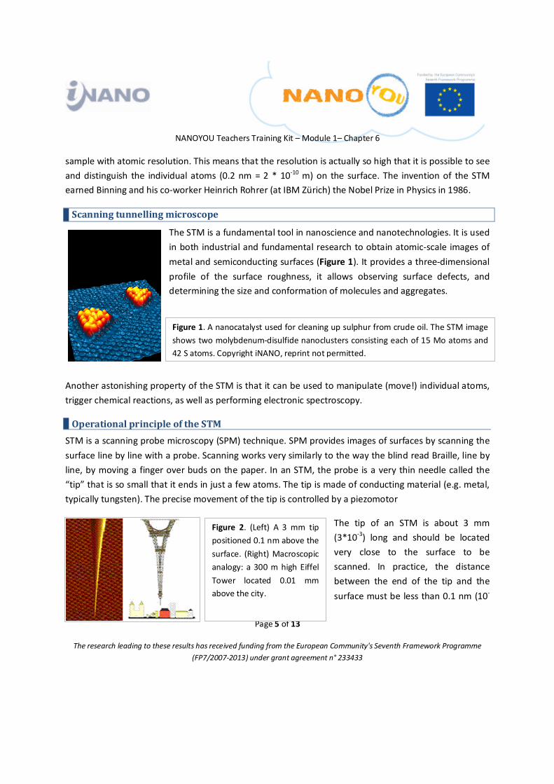
Scanning tunnelling microscope
The STM is a fundamental tool in nanoscience and nanotechnologies. It is used
in both industrial and fundamental research to obtain atomic-scale images of
metal and semiconducting surfaces (Figure 1). It provides a three-dimensional
profile of the surface roughness, it allows observing surface defects, and
determining the size and conformation of molecules and aggregates.
Another astonishing property of the STM is that it can be used to manipulate (move!) individual atoms,
trigger chemical reactions, as well as performing electronic spectroscopy.
Operational principle of the STM
STM is a scanning probe microscopy (SPM) technique. SPM provides images of surfaces by scanning the
surface line by line with a probe. Scanning works very similarly to the way the blind read Braille, line by
line, by moving a finger over buds on the paper. In an STM, the probe is a very thin needle called the
“tip” that is so small that it ends in just a few atoms. The tip is made of conducting material (e.g. metal,
typically tungsten). The precise movement of the tip is controlled by a piezomotor
The tip of an STM is about 3 mm
(3*10-3
) long and should be located
very close to the surface to be
scanned. In practice, the distance
between the end of the tip and the
surface must be less than 0.1 nm (10-
Figure 1. A nanocatalyst used for cleaning up sulphur from crude oil. The STM image
shows two molybdenum-disulfide nanoclusters consisting each of 15 Mo atoms and
42 S atoms. Copyright iNANO, reprint not permitted.
NANOYOU Teachers Training Kit – Module 1– Chapter 6
Page 6 of 13
The research leading to these results has received funding from the European Community's Seventh Framework Programme
(FP7/2007-2013) under grant agreement n° 233433
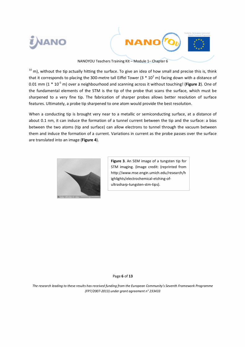
Figure 3. An SEM image of a tungsten tip for
STM imaging. (Image credit: (reprinted from
http://www.mse.engin.umich.edu/research/h
ighlights/electrochemical-etching-of-
ultrasharp-tungsten-stm-tips).
10 m), without the tip actually hitting the surface. To give an idea of how small and precise this is, think
that it corresponds to placing the 300-metre tall Eiffel Tower (3 * 102 m) facing down with a distance of
0.01 mm (1 * 10-5 m) over a neighbourhood and scanning across it without touching! (Figure 2). One of
the fundamental elements of the STM is the tip of the probe that scans the surface, which must be
sharpened to a very fine tip. The fabrication of sharper probes allows better resolution of surface
features. Ultimately, a probe tip sharpened to one atom would provide the best resolution.
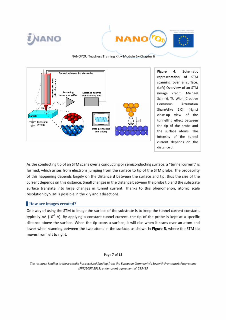
When a conducting tip is brought very near to a metallic or semiconducting surface, at a distance of
about 0.1 nm, it can induce the formation of a tunnel current between the tip and the surface: a bias
between the two atoms (tip and surface) can allow electrons to tunnel through the vacuum between
them and induce the formation of a current. Variations in current as the probe passes over the surface
are translated into an image (Figure 4).
NANOYOU Teachers Training Kit – Module 1– Chapter 6
Page 7 of 13
The research leading to these results has received funding from the European Community's Seventh Framework Programme
(FP7/2007-2013) under grant agreement n° 233433
Figure 4. Schematic
representation of STM
scanning over a surface.
(Left) Overview of an STM
(Image credit: Michael
Schmid, TU Wien, Creative
Commons Attribution
ShareAlike 2.0); (right)
close-up view of the
tunnelling effect between
the tip of the probe and
the surface atoms. The
intensity of the tunnel
current depends on the
distance d.
As the conducting tip of an STM scans over a conducting or semiconducting surface, a “tunnel current” is
formed, which arises from electrons jumping from the surface to tip of the STM probe. The probability
of this happening depends largely on the distance d between the surface and tip, thus the size of the
current depends on this distance. Small changes in the distance between the probe tip and the substrate
surface translate into large changes in tunnel current. Thanks to this phenomenon, atomic scale
resolution by STM is possible in the x, y and z directions.
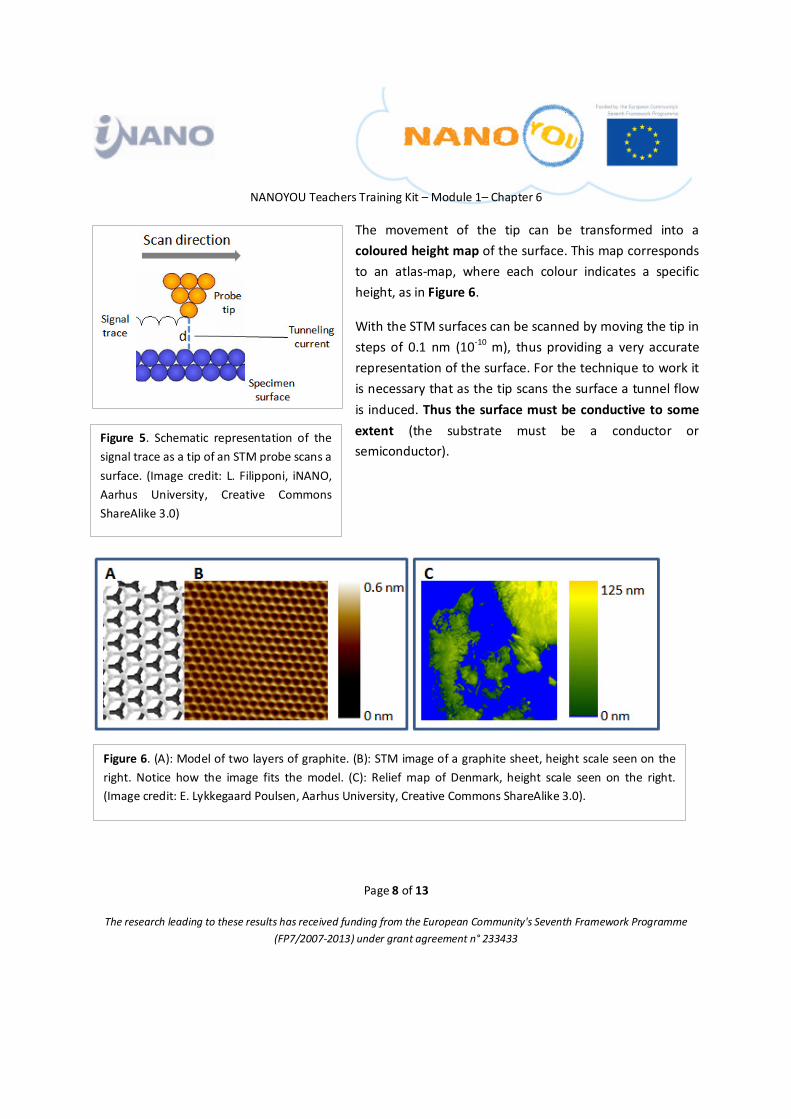
How are images created?
One way of using the STM to image the surface of the substrate is to keep the tunnel current constant,
typically nA (10-9
A). By applying a constant tunnel current, the tip of the probe is kept at a specific
distance above the surface. When the tip scans a surface, it will rise when it scans over an atom and
lower when scanning between the two atoms in the surface, as shown in Figure 5, where the STM tip
moves from left to right.
NANOYOU Teachers Training Kit – Module 1– Chapter 6
Page 8 of 13
The research leading to these results has received funding from the European Community's Seventh Framework Programme
(FP7/2007-2013) under grant agreement n° 233433
Figure 5. Schematic representation of the
signal trace as a tip of an STM probe scans a
surface. (Image credit: L. Filipponi, iNANO,
Aarhus University, Creative Commons
ShareAlike 3.0)
Figure 6. (A): Model of two layers of graphite. (B): STM image of a graphite sheet, height scale seen on the
right. Notice how the image fits the model. (C): Relief map of Denmark, height scale seen on the right.
(Image credit: E. Lykkegaard Poulsen, Aarhus University, Creative Commons ShareAlike 3.0).
The movement of the tip can be transformed into a
coloured height map of the surface. This map corresponds
to an atlas-map, where each colour indicates a specific
height, as in Figure 6.
With the STM surfaces can be scanned by moving the tip in
steps of 0.1 nm (10-10
m), thus providing a very accurate
representation of the surface. For the technique to work it
is necessary that as the tip scans the surface a tunnel flow
is induced. Thus the surface must be conductive to some
extent (the substrate must be a conductor or
semiconductor).
NANOYOU Teachers Training Kit – Module 1– Chapter 6
Page 9 of 13
The research leading to these results has received funding from the European Community's Seventh Framework Programme
(FP7/2007-2013) under grant agreement n° 233433
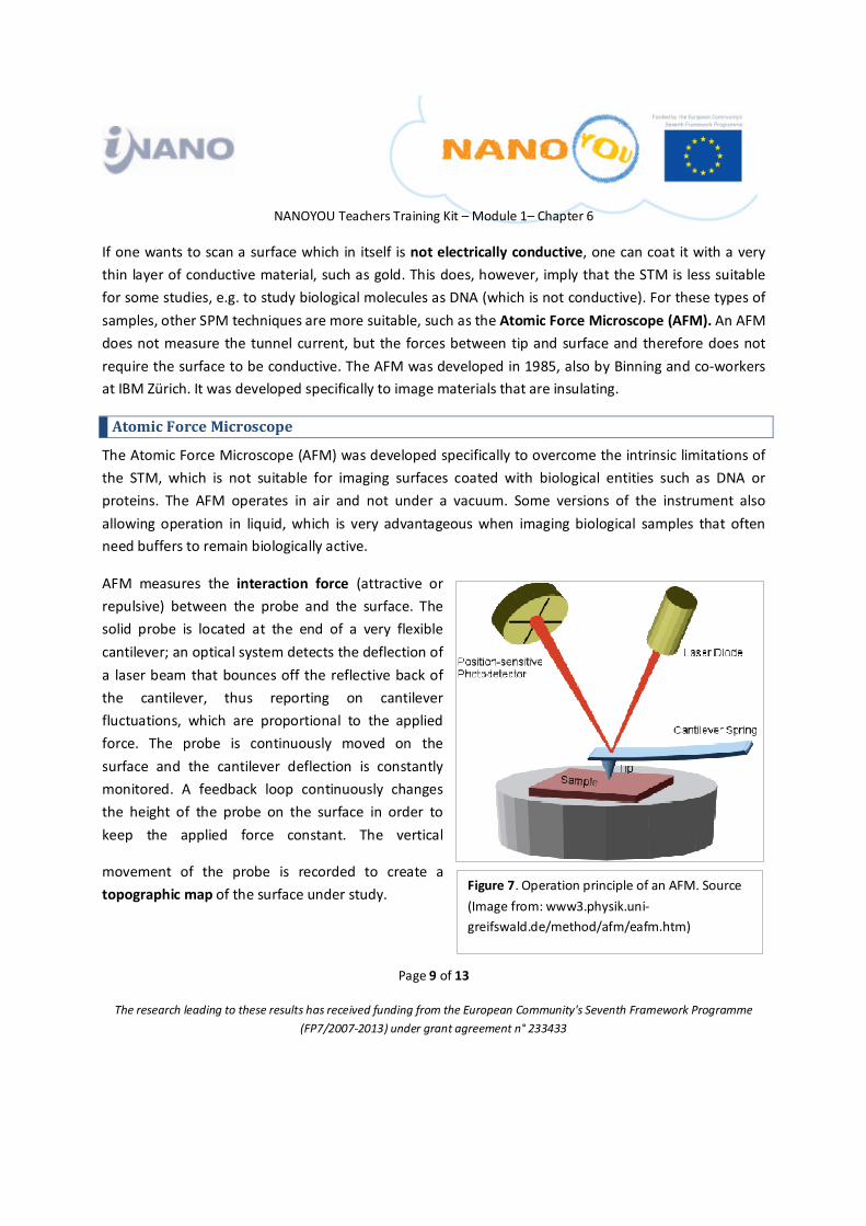
Figure 7. Operation principle of an AFM. Source
(Image from: www3.physik.uni-
greifswald.de/method/afm/eafm.htm)
If one wants to scan a surface which in itself is not electrically conductive, one can coat it with a very
thin layer of conductive material, such as gold. This does, however, imply that the STM is less suitable
for some studies, e.g. to study biological molecules as DNA (which is not conductive). For these types of
samples, other SPM techniques are more suitable, such as the Atomic Force Microscope (AFM). An AFM
does not measure the tunnel current, but the forces between tip and surface and therefore does not
require the surface to be conductive. The AFM was developed in 1985, also by Binning and co-workers
at IBM Zürich. It was developed specifically to image materials that are insulating.
Atomic Force Microscope
The Atomic Force Microscope (AFM) was developed specifically to overcome the intrinsic limitations of
the STM, which is not suitable for imaging surfaces coated with biological entities such as DNA or
proteins. The AFM operates in air and not under a vacuum. Some versions of the instrument also
allowing operation in liquid, which is very advantageous when imaging biological samples that often
need buffers to remain biologically active.
AFM measures the interaction force (attractive or
repulsive) between the probe and the surface. The
solid probe is located at the end of a very flexible
cantilever; an optical system detects the deflection of
a laser beam that bounces off the reflective back of
the cantilever, thus reporting on cantilever
fluctuations, which are proportional to the applied
force. The probe is continuously moved on the
surface and the cantilever deflection is constantly
monitored. A feedback loop continuously changes
the height of the probe on the surface in order to
keep the applied force constant. The vertical
movement of the probe is recorded to create a
topographic map of the surface under study.
NANOYOU Teachers Training Kit – Module 1– Chapter 6
Page 10 of 13
The research leading to these results has received funding from the European Community's Seventh Framework Programme
(FP7/2007-2013) under grant agreement n° 233433
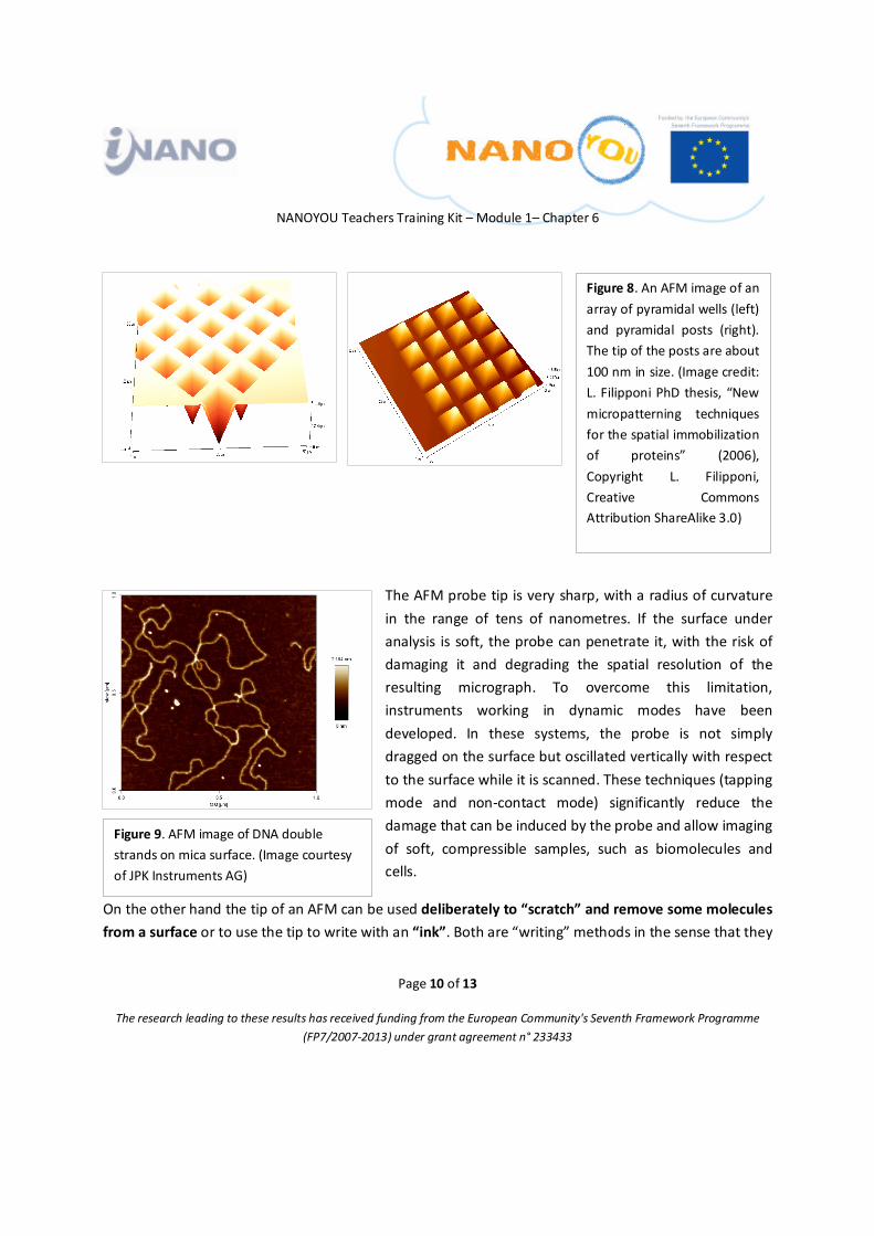
Figure 8. An AFM image of an
array of pyramidal wells (left)
and pyramidal posts (right).
The tip of the posts are about
100 nm in size. (Image credit:
L. Filipponi PhD thesis, “New
micropatterning techniques
for the spatial immobilization
of proteins” (2006),
Copyright L. Filipponi,
Creative Commons
Attribution ShareAlike 3.0)
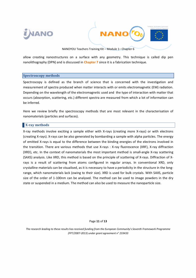
Figure 9. AFM image of DNA double
strands on mica surface. (Image courtesy
of JPK Instruments AG)
The AFM probe tip is very sharp, with a radius of curvature
in the range of tens of nanometres. If the surface under
analysis is soft, the probe can penetrate it, with the risk of
damaging it and degrading the spatial resolution of the
resulting micrograph. To overcome this limitation,
instruments working in dynamic modes have been
developed. In these systems, the probe is not simply
dragged on the surface but oscillated vertically with respect
to the surface while it is scanned. These techniques (tapping
mode and non-contact mode) significantly reduce the
damage that can be induced by the probe and allow imaging
of soft, compressible samples, such as biomolecules and
cells.
On the other hand the tip of an AFM can be used deliberately to “scratch” and remove some molecules
from a surface or to use the tip to write with an “ink”. Both are “writing” methods in the sense that they
NANOYOU Teachers Training Kit – Module 1– Chapter 6
Page 11 of 13
The research leading to these results has received funding from the European Community's Seventh Framework Programme
(FP7/2007-2013) under grant agreement n° 233433
allow creating nanostructures on a surface with any geometry. This technique is called dip pen
nanolithography (DPN) and is discussed in Chapter 7 since it is a fabrication technique.
Spectroscopy methods
Spectroscopy is defined as the branch of science that is concerned with the investigation and
measurement of spectra produced when matter interacts with or emits electromagnetic (EM) radiation.
Depending on the wavelength of the electromagnetic used and the type of interaction with matter that
occurs (absorption, scattering, etc.) different spectra are measured from which a lot of information can
be inferred.
Here we review briefly the spectroscopy methods that are most relevant in the characterisation of
nanomaterials (particles and surfaces).
X-ray methods
X-ray methods involve exciting a sample either with X-rays (creating more X-rays) or with electrons
(creating X-rays). X-rays can be also generated by bombarding a sample with alpha particles. The energy
of emitted X-rays is equal to the difference between the binding energies of the electrons involved in
the transition. There are various methods that use X-rays : X-ray fluorescence (XRF), X-ray diffraction
(XRD), etc. In the context of nanomaterials the most important method is small-angle X-ray scattering
(SAXS) analysis. Like XRD, this method is based on the principle of scattering of X-rays. Diffraction of X-
rays is a result of scattering from atoms configured in regular arrays. In conventional XRD, only
crystalline materials can be visualised, as it is necessary to have a periodicity in the structure in the long-
range, which nanomaterials lack (owing to their size). XRD is used for bulk crystals. With SAXS, particle
size of the order of 1-100nm can be analysed. The method can be used to image powders in the dry
state or suspended in a medium. The method can also be used to measure the nanoparticle size.
NANOYOU Teachers Training Kit – Module 1– Chapter 6
Page 12 of 13
The research leading to these results has received funding from the European Community's Seventh Framework Programme
(FP7/2007-2013) under grant agreement n° 233433
UV-Visible plasmon absorption and emission
Metal nanoparticles, in particular gold and silver, are characterised by a plasmon resonance absorption
that gives rise to intensely coloured solutions.
The fundamentals of the plasmon resonance effect are described in Chapter 4 of Module
1 “Fundamental “nano-effects”.
The absorption band is due to electrons confined at the particle surface that collectively oscillate at a
specific frequency, commonly referred to as the surface plasmon resonance frequency. To give some
examples, the plasmon band of a 20 nm silver (Ag) particle is centred at 395 nm, resulting in a yellow
solution, while a 20 nm gold (Au) particle absorbs at 520 nm resulting in a red solution. The plasmon
absorption effect occurs for particles up to approx. 50 nm in diameter and scales with particle volume.
Absorption can in be in the visible and UV area of the spectrum. Particles can be visualised by
absorbance in solution at nanomolar and picomolar concentrations.
Plasmon resonance light scattering
In larger metal nanoparticles (>30 nm) another effect, light scattering, is observed. When illuminated
with white light, metal nanoparticles in the 50-120 nm diameter size range scatter light of a specific
colour at the surface plasmon resonance frequency. This effect is called plasmon resonance light
scattering. As in the case of plasmon absorbance, light scattering scales with particle volume, but the
scattered light can be detected at much lower concentrations than absorbed light. For example, light
scattered by a solution of 80 nm diameter gold particles is detectable down to 5 fM concentration (fM=
10-15
M). For this reason metal nanoparticles are interesting materials for use in techniques that rely on
labelling (such as microarray technology).
Metal nanoparticles are also described in Chapter 5 “Overview of Nanomaterials” of
Module 1, and their application to the medical sector is described in Chapter 1
“Application of Nanotechnologies: Medicine and Healthcare” of Module 2.
NANOYOU Teachers Training Kit – Module 1– Chapter 6
Page 13 of 13
The research leading to these results has received funding from the European Community's Seventh Framework Programme
(FP7/2007-2013) under grant agreement n° 233433
Surface-Enhanced Raman Scattering
Metal surfaces with nanometre scale roughness have the property of amplifying the Raman scattering
signals of absorbed molecules. In simple words, Raman scattering is the inelastic scattering of photons.
Normally, when light is scattered from an atom or molecule, it has the same energy (frequency) and
wavelength as the incident light (Rayleigh scattering). This is an elastic scattering. However, a small
fraction of the scattered light (approximately 1 in 10 million photons) is scattered by an excitation, with
the scattered photons having energy (frequency) different from the frequency of the incident photons.
Metal surfaces with nanoscale roughness increase the Raman scattering of molecules absorbed on
them. This effect is due to chemical and electromagnetic factors, as well as increased surface area. We
will not go into the details of this effect: what is important is that the SERS effect can induce a signal
enhancement of up to 108 times. In one specific case it has been possible to achieve a Raman
enhancement effect of 1015
times! This means that the SERS effect makes it possible to push the
detection limit of surface detection techniques. The SERS signal depends on the characteristics of the
nano-substrate: the size, shape, orientation and composition of the surface nano-roughness.
Advancement in SERS technology will allow detection at the attomole (10-18 mol) level, and single
molecule detection.
Non-radiative and non-electron characterisation methods
There are numerous methods to characterise nanomaterials which do not rely on the use of an EM
radiation. They include methods to determine particle size, surface area and porosity; thermodynamic
methods (such as thermogravimetric analysis, TGA) to evaluate the temperature dependence of the
nanomaterial (melting, etc.); and mass spectroscopy, to determine the chemical composition of the
nanomaterial. An important surface method is the quartz crystal microbalance (QCM), which can
measure mass changes as small as a few nanograms per square centimetre. This is sensitive enough to
detect monolayers of deposited materials. It can be used to measure the amount of metal deposited on
a surface after sputtering or evaporation, or to measure the amount of protein absorbed on a surface.
Due to this great sensitivity, the QCM is used in the design of biosensors.


