CHAPTER 4
PWM STRATEGIES FOR INVERTERS WITH
FLUCTUATING DC LINK INPUT
4.1 INTRODUCTION
The modified SPWM control schemes (MSPWM-T and MSPWM-S) [59] have
served to achieve the desired fundamental and eliminate lower order hannonic
components caused by the dc voltage source fluctuation. However, these analog based
solutions are effective only at high switching frequencies and resulted in higher
switching losses. besides being indirect in nature.
It is normally assumed that the dc-link is a perfect constant dc voltage.
However. in a practical system. it contains ripple components due to the rectification
process. An analysis of the power conversion process shows that the power at the dc-
link consists of constant active power as well as a pulsating component that fluctuates
at twice the mains frequency. When a VSI is powered by the fluctuating dc-link
voltage. it generates additional subharmonics because of the modulation heween the
inverter switching function and the dc-link ripple [97]. Moreover. the ripple in the
dc-link is the primary contributor for the appearance of harmonics in the inverter output
not present in the PWM switching function 1981 and is responsible for the deterioration
in the quality of the output voltage. Further the harsh loads on the invener power
supply contrihutc to wa\.eform distortion and intmduce abnormal harmonics in the
invener input current. The switching action further creates ripples at the dc-link.
The input voltage distonion in a voltage source PWM controlled invener will
limit the amplitude of the fundamental and i n d u c e unexpected lower order
harmonics 1561. The use of conventional harmonic duction techniques ends up onl!
with the reappearance of the lower order harmonics in the output waveform. It is only
appropriate that the next generation PWM modulators for inverters he inherently capahle
of rejecting the dc-link voltage ripple to offer a higher quality of output voltage.
Therefore. there is a need to innoviur a P'H'M switching strategy. which offers an
enhanced performance compared to existing methods in terms of minimal lower order
harmonics, reduced THD and enhanced fundamental, especially at low switching
frequencies.
4.2 PROBLEM FORMULATION
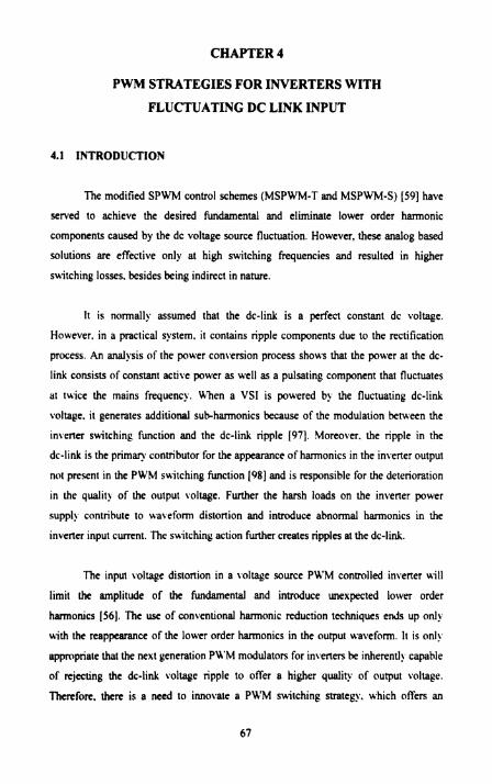
The distoned input due to the improper value of dc-link capacitor in an ac-ac
PWM conversion system introduces lower order harmonics and increases the THD [56],
as seen in Fig.4.1. The objective is to develop a low frequency. PPWM strategy. which
will render an improved performance in terms of minimal lower order harmonics and
reduced THD for inverters with fluctuating dc input. A new P W M technique is
proposed for a single-phase inverter to reduce the lower order harmonics caused by the
fluctuating dc input. The width of the PWM pulses in this approach is determined by
making the area of the PWM signal equal to that under the sampled reference
waveform.
Fig.4.I Ourput voltage and frequency spectrum of SPFB with fluctuating dc input
(V,=230V, C=23.5cF)
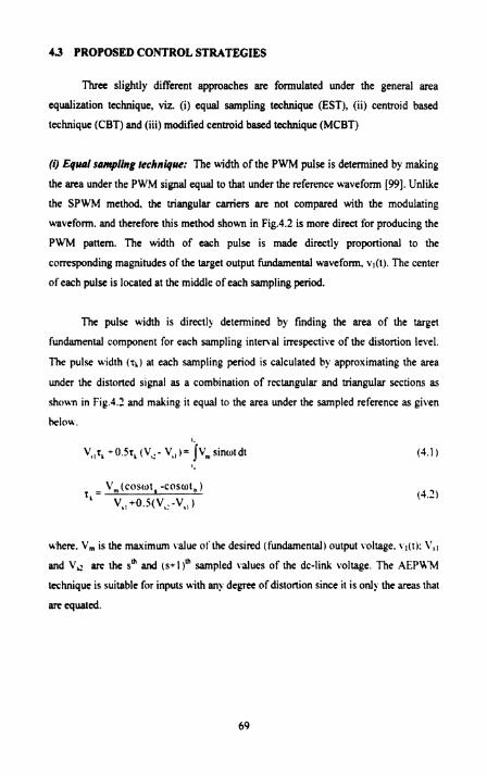
4 3 PROPOSED CONTROL STRATEGIES
Three slightly different approaches are formulated under the general area
equalization technique, viz. (i) equal sampling technique (EST), (ii) centroid based
technique (CBT) and (iii) modified centroid based technique (MCBT)
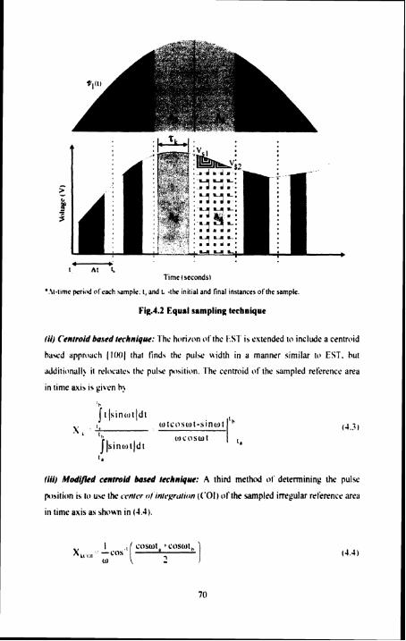
(i) Equd sonrpling technique: The width of the PWM pulse is determined by making
the area under the PWM signal equal to that under the reference waveform 1991. Unlike
the SPWM method. the triangular caniers are not compared with the modulating
waveform. and therefore this method shown in Fig.4.2 is more direct for producing the
PWM pattern. The width of each pulse is made directly proportional to the
corresponding magnitudes of the target output fundamental waveform, vl(t). The center
of each pulse is located at the middle of each sampling period.
The pulse width is direct11 determined by finding the area of the target
fundamental component for each sampling intenal irrespective of the distortion level.
The pulse width (16) at each sampling period is calculated by approximating the area
under the distorted signal as a combination of rectangular and triangular sections as
shoun in Fig.4.2 and making it equal to the area under the sampled reference as given
k l o n .
where, V, is the maximum value ot'the desired (fundamental) output voltage. vl(t): V, ,
and VQ are the sh and ( s + l ) ~ sampled values of the dc-link voltage. The AEPWU
technique is suitable for inputs with any degree of distortion since it is only the areas that
arc equated.
-' I A1 1
Time I seconds)
' 1l.11rnc prsd of each \ample. I, and L -the lnlt~al and linal Instances of the sample
Fig.4.2 Equal sampling technique
(ii) Centroid basedrechnique: 'The horimn of the ItS'1 is extended to include a cmtriiid
bawd appniach I lo()/ that finds the pulw width in u manner similar to EST. hut
additionall) it reltratc* the pulw yosition. I'he centroid of the sampled wfertncc area
in time avir is given h!
Mi) Modl/lcd centroid &mi technique: A third method 01' determining the pulse
position is IO use the n~nrcSr r t t inrc.grurion (('01) nt'the sampled irregular wl'erence area
in time axis as shwvn in (4.4).

4.4 SIMULATION RESULTS
When the inverter is connected to the rectifier, the filtered output is
superimposed with high frequency ripples in addition to the distortions due to
insufficient filtering. The circuit conditions are ac input=230V, capacitor, C=23.5~F and
pulse number per cycle, r4O. The simulation is performed using Matlab. The results
presented are chosen to provide a comparative basis for evaluating the performance of
AEPWM techniques. The switching patterns are generated so as to provide a
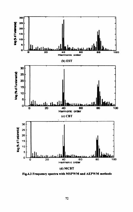
fundamental ac output of 255V. Fig.4.3 shows the frequency spectra with AEPWM
techniques. which substantiates that the lower order harmonic components are almost
less than five percent and hence within acceptable limits. Further it follows that the
PWM panem obtained using AEPWM techniques will enable the invener to generate a
much bener spectra of output compared to the analog based MSPWM.
The SPWM and MSPWM methods are compared uith the AEPWM methods for
the fundamental (V,). lower order harmonics (Vj. V5 and V:) and M D in Table 4.1.
Thew is a considerable increase in the fundamental; the lower order harmonics are
significantly reduced besides a marginal reduction in THD in the AEPWM methods.
m a r l c - (a) MSPWM
30
1: 1 16
'6 C 10 P 2 6
0 0 20 40 80 BO 1 0 0
Harmcnlc mhr
(c) CBT
H a m l c order
(d) MCBT
Fig.4.3 Frequency spectra witb MSPWM and AEP'H'M methods
Table 4.1 Compariwn of SPWM, MSPWM and AEPWM methods
4.5 HARDWARE IMPLEMENTATION
With the availability of low cost DSP chips. characterized by improved
performance, high speed and reduced instruction ser computing (RISC). complicated
control algorithms can be executed in real-time. offering a high sampling rate for
digitally?controlled inverters [I 01. 1021.
The Texas instruments TMS320LF2407 DSP [I031 controller (refirred ro as
LF?JO') is a programmable digital controller with a C2XX DSP cenrral processing
rrnir (CPl.1) as he core processor. The LF2407 contains the DSP core processor and
useful peripherals integrated onto a single piece of silicon. It combines the powerful
CPLI with an on-chip memon and peripherals. I t has a 16 bit fixed point arithmetic
unit. a 40MHz CPLJ clock and several peripherals such as even! manager (EL').
con~roller trrc8u mwork (CAN) interface. serial perbheral inrerface (SPl). .vrrial
communicariunr inr~~tfuce (SCI) and ADC modules. The 240x series of TI DSP
combines this real-time processing capability with controller peripherals to create an
ideal environment for control applications. The peripherals in the LF2107 enable
virtually any application possible in the rdnge from analog to digital conversion to
PWM generation. The LF2407 peripheral set includes two EVs, general purpose timers,
PWM generators, CAN, analog-to-digital converter, SPI port, SCI-asynchronous serial
port, watchdog timer and general-purpose bidirecrio~l digital I/O (GPIO) pins.
The two EVs (EV Am) in the board are identical to one another in terms of
functionality and registerhit definition, but have different register names and addresses.
Each EV has its own local interrupt subsystem, which includes its own intermpt mask
and flag registers. There are two general-purpose (GP) timers in each module. The full
compare units (I, 2 &3) and (4, 5 & 6) in EVA and EVB modules respectively; enable
logging of transitions on capture input pins. The value of the GP timer 1 counter is
continuously compared with that of the compare register. When a match is achieved, a
transition appears on the two outputs of the compare unit according to the bits in the
action ronrral register (ACTRA). The outputs of the compare units in the compare
mode are subject to modification by the output logic, dead band units. and the SVPWM
logic.
The proposed dc-link fluctuation compensation method is tested on a SPFB
inverter system. built using IRF840 MQSFET devices. The uncontrolled rectifier is
realised by 6A4 MIC diodes. The rectified output through a filter capacitance serves as
an input to the in~ener. The LF2407 has the necessary features to a l l o ~ easy
~mplementation of AEPWM techniques in an invener with distorted dc input. The input
is sensed accuratel! and fed to the DSP controller through a hall-effect voltage sensor
I.V25-PI4048 seen in Fig.4.4. The closed loop model of the arrangement is sho~m in
Fig.4.S.

Fig.4.4 LV25-P 14048 voltage sensor
Rect~f~er Inverter
DSP Control -- --
Fig.4.5 Block diagram of a closed loop digitalb controlled ac-ac s?stem
The SPWM is a pulse train generated diictly by comparing a sinusoidal
reference signal with a camer signal of higher frequency. The effectiveness in digital
implementation of SPWM lies in efficient reproducing of look-up-table (LUT) based
natural sampled functions. The flow chart of the algorithm of SPWM generation is
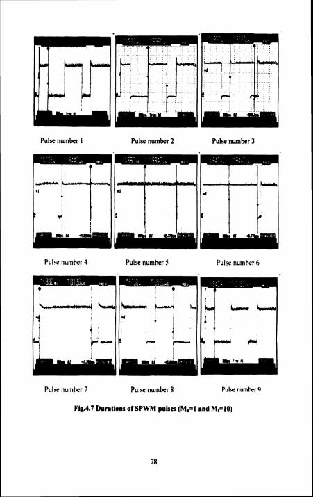
s h o w in Fig.4.6. The effectiveness of the algorithm in generating SPWM pulses for a
typical M. and Mr values are demonstrated in Fig.4.7 and verified in Table 4.2. The
SPWM and EST techniques use the timer continuous up mode while CBT and MCBT
use continuous upldown mode due to the requirement of loading two counts in between
overflow and underflow. The LF2407 registers are initialised in a manner similar to as
that for the SPWM method. The pulse widths and the pulse positions are computed
such that they match the LF2407 timer values and stored in compare unit buffer
register. The timer period (TIPR) for the EST method is loaded with 19200 for z=20
according to the equation (4.5).
TI PR value = Desired PWM period
2 (GP timer prescaled clock period)
The values of TlPR for CBT and MCBT are loaded with 38400 for ~ 2 0 according to
the equalion (4.6).
TI PR value = Desired P b N period
GP timer prescaled clock period
The PWM pulses are generated when a compare match occurs as set by the
ACTRA. l h e PWM channels of the event manager in the LF2407 are used to generate
the pulses. The PWM pins PWMI. PWM?. PWM3 and PWM4 are used to trigger the
inverter switches.
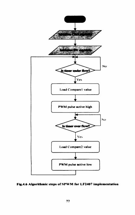
Lxmd Compare l value k PWM pulse active high ?
L I ~ Compare2 value
PWM pulse active low r-l Fig.4.6 Algorithmic steps of SPWM for LF2-7 implementation
77
Pulse number I Pulse number 2 Pulse number 3
Pulw numhc'r 1 Pulse numher ! Pulse number 6
Pulsc number 7 Pulx number 8 Pulw numher 9
Fig.4.7 Durations of SPWM pulses ( M . 4 and M p l O )

Fig.4.8 Experimental arrangement of AEPWM implementation in SPFB
Tablc 4.2 Accuracy of generated SPWM pulse durntions
Pulse number Pulse width
312
3 '7 4!6 942
988 984
I'he espurimental wsults are obtained for an ac input voltage of 23OV using the
arrangement shown in 1:iy.l.X. The dc-link toltage ripple for a capacitor value of
23.SpF i h li~und 11) k tilt! percent as shown in Fig.4.9. The in\erter output voltage
wa\cforms ~ i t h 1:ST Ibr the same capacitor d u e is sho\tn in I:ig.l.lO and the
hquenc ) sprctnl with SPWM and the AEPWM methods are gi\en in Fiy.4.I 1. It is
found that the dc-link voltage is considerably dislurkd in compliance with the
frequent) of the PU'M signal. The voltage spectrum ohtained uith SPWM illustrates
that lower order harmonics are introduced in the output voltage. The frequcnc! spectra
with Alf'U'M techniques suhstantiate the close comparison ol' esperimental and
simulated performances in terms ol'rcduced lower order harmonics. I'ahle 4.3 \.alidates
the efTec~iveness ofthe 1)SP hased implementation ofthe pmpogd strategies.

Fig.4.9 Fluctuation in dc-link voltage
lWA
Z d n
Fig.4.10 Inverter output voltage with EST
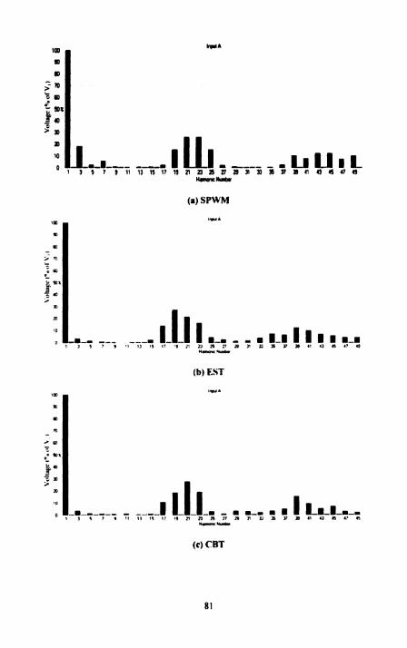
(a) SPWM
(h) EST
(c) CBT
81

(d) MCBT
Fig.4.11 Frequency spectra of experimentally obtained output voltages
Thc invencr output vc~ltage obtained using the AEPWM (EST) method with out
a dc-link capacitor is shown in I:ig.J.I?. Fig.J.l3(a) and t'ig.4.13(h) funher highligh! the
Fact that the s>stern can work even without the capacitor. hesides allowing a saving in
space without an! compmmise on rrliahilit! and life time of the system even at higher
ambien! temperatures. 'lahlc 4.4 depicts comparison of lower order harmonics and THD
ol'SPH'M and 1:s-I fbr without the dc-link capacitor.
Input A 1 ,
Fig.4.12 Inverter output voltage with EST, without dc-link capacitor

Table 4.3 Comparison of AEPWM methods
I...... . ....I.... II .. +..I. II I a,.... .. I 5 9 v n a a n n 1 7 ~ 1 r s r s
(a) SPWM (b) EST
Fig.J.13 Frequency spectra with SPWM and EST without dc-link capacitor
Table 4.4 Comparison of lower order barmonics and THD without dc-link capacitor
I Y3 / VI j I
v7 Techniques I THD
67.93
59.1 I
I ( O h of V,)
SPWM
EST
2.8
1.7
27.2
1.3
11.4
1.2

4.6 SUMMARY
The AEPWM techniques have served to provide compensation for the PWM
inverters working with fluctuating dc input. The lower order harmonic components,
which increase the filter size and Cost, are well reduced by using AEPWM techniques.
The proposed AEPWM methods are a low switching 'equency solution to the dc
voltage fluctuation, thus reducing the switching losses. The simulation results have
revealed the superiority of the proposed strategy over the existing MSPWM. The
experimental solutions that compares closely with the simulated results indicate that this
approach can be implemented in a digital platform even in a fluctuating dc environment.
The implemented srmtegy has brought out the suitability of the schemes for applications
such as aircraft power supplies; UPS in computer system, traction drives, and drives for
communication satellites and launch vehicles.


