Bringing THz communication to the mass market:
no longer an illusion?Piet Wambacq, imec Fellow and professor at VUB, Brussels
with thanks to many imec colleagues
public
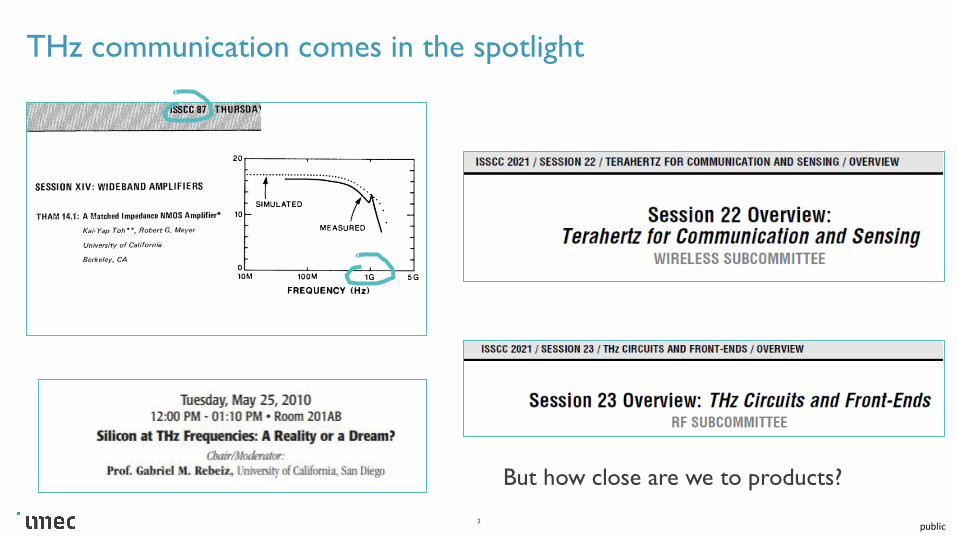
THz communication comes in the spotlight
2
But how close are we to products?

public
D-band integrated circuits coming to maturity
3
Transceiver functionality, efficient power amplifiers, ...
Imec, 140GHz BiCMOS PA, ESSCIRC 2019
34 dB gain, Psat of 17 dBm with 13% PAE
1.76mm
0.6
mm
130nm BiCMOS
Can we make mass markets 6G
systems with these circuits?
2019
6.5mm2 SISO TRx chip
1X4 MIMO module 16 GHz FMCW PLL
imec, 40GHz radar transceiver 28nm CMOS
Nokia, European 5G Conference 2021
public
6G
4
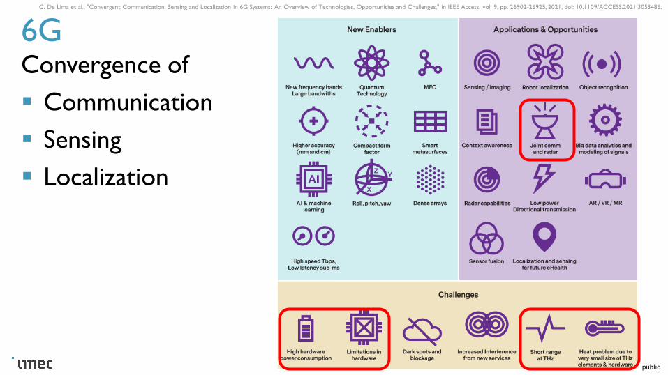
C. De Lima et al., "Convergent Communication, Sensing and Localization in 6G Systems: An Overview of Technologies, Opportunit ies and Challenges," in IEEE Access, vol. 9, pp. 26902-26925, 2021, doi: 10.1109/ACCESS.2021.3053486.
Convergence of
▪ Communication
▪ Sensing
▪ Localization
public
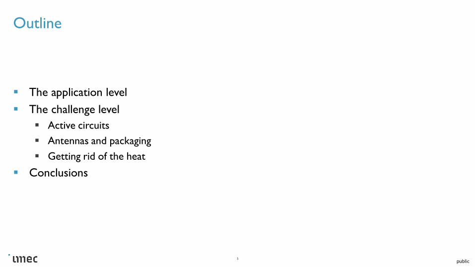
Outline
▪ The application level
▪ The challenge level
▪ Active circuits
▪ Antennas and packaging
▪ Getting rid of the heat
▪ Conclusions
5
public
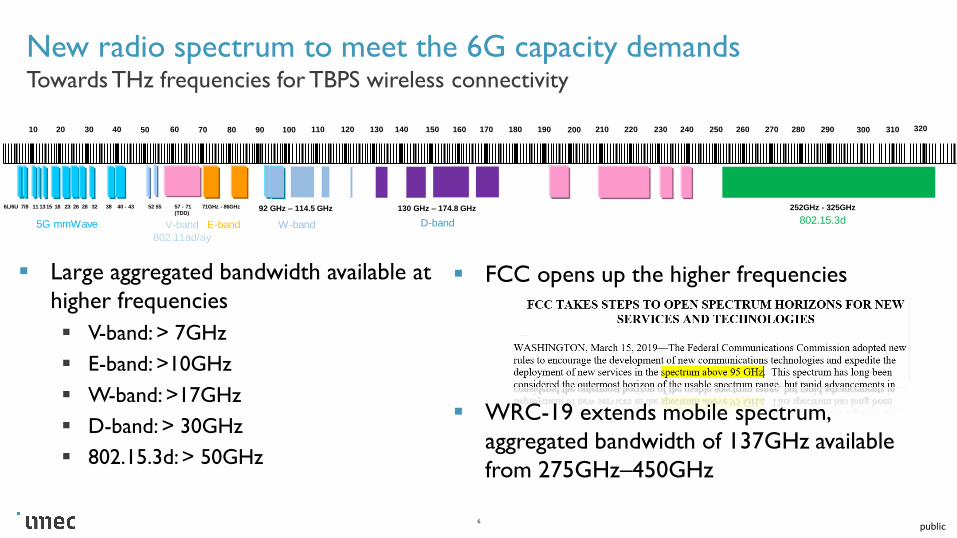
New radio spectrum to meet the 6G capacity demands
▪ Large aggregated bandwidth available at
higher frequencies
▪ V-band: > 7GHz
▪ E-band: >10GHz
▪ W-band: >17GHz
▪ D-band: > 30GHz
▪ 802.15.3d: > 50GHz
6
Towards THz frequencies for TBPS wireless connectivity
6L/6U
10010 20 30 40 50 60 70 80 90
11 13 15 18 23 26 38 71GHz - 86GHz7/8 40 - 43 52 55 57 - 71
(TDD)
28 32
200110 120 130 140 150 160 170 180 190 300210 220 230 240 250 260 270 280 290
252GHz - 325GHz92 GHz – 114.5 GHz 130 GHz – 174.8 GHz
310 320
5G mmWave V-band
802.11ad/ay
E-band W-band D-band 802.15.3d
▪ FCC opens up the higher frequencies
▪ WRC-19 extends mobile spectrum,
aggregated bandwidth of 137GHz available
from 275GHz–450GHz
public
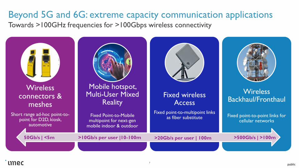
Beyond 5G and 6G: extreme capacity communication applications
7
Towards >100GHz frequencies for >100Gbps wireless connectivity
Wireless connectors &
meshes
Short range ad-hoc point-to-point for D2D, kiosk,
automotive
Mobile hotspot, Multi-User Mixed
Reality
Fixed Point-to-Mobile multipoint for next-gen
mobile indoor & outdoor
Fixed wireless Access
Fixed point-to-multipoint links as fiber substitute
Wireless Backhaul/Fronthaul
Fixed point-to-point links for cellular networks
50Gb/s | <5m >10Gb/s per user |10-100m >20Gb/s per user | 100m >500Gb/s | >100m
public
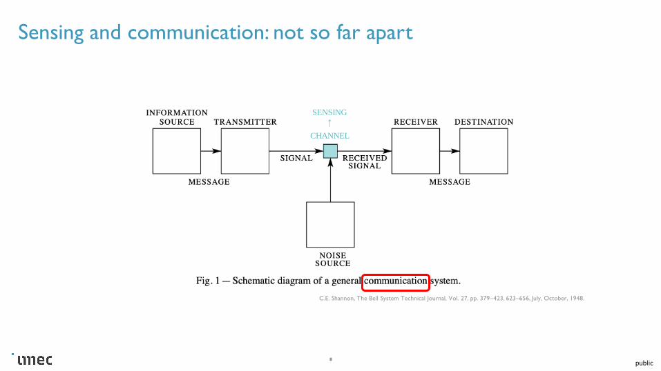
Sensing and communication: not so far apart
8
CHANNEL
SENSING
↑
C.E. Shannon, The Bell System Technical Journal, Vol. 27, pp. 379–423, 623–656, July, October, 1948.

public
In sensing the channel is the message
9
CHANNEL
ENCODER
↑
M. McLuhan, “Understanding Media: The Extensions of Man”, MIT Press, 1994.
sensing
ILLUMINATOR
public
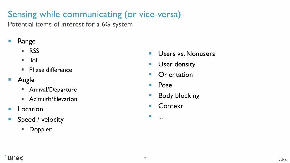
Sensing while communicating (or vice-versa)
▪ Range
▪ RSS
▪ ToF
▪ Phase difference
▪ Angle
▪ Arrival/Departure
▪ Azimuth/Elevation
▪ Location
▪ Speed / velocity
▪ Doppler
10
Potential items of interest for a 6G system
▪ Users vs. Nonusers
▪ User density
▪ Orientation
▪ Pose
▪ Body blocking
▪ Context
▪ ...

public
WiFi-based passive bistatic radars
11
Opportunistic use of known preambles
L. Storrer, H. C. Yildirim, C. Desset, M. Bauduin, A. Bourdoux and F. Horlin, "Clutter removal for Wi-Fi-based passive bistatic radar," 2020 IEEE 91st Vehicular Technology Conference (VTC2020-Spring), Antwerp, Belgium, 2020, pp. 1-5
Need for clutter removal, extensice to 160MHz

public
6G PHY design
▪ Non Uniform Multiband OFDM THz
▪ Combine distance and sensing accuracy, using
multiple OFDM waveforms
▪ Non-uniform subcarrier spacing parameters
▪ long detectable distance from the small
subcarrier spacing
▪ high sensing accuracy from the large subcarrier
spacing.
▪ 100 Gbps and sub-mm ranging
12
Taking into account sensing requirements from the start
▪ SI-DFT-s-OFDM
▪ Sensing integrated joint design allows for mm
scale ranging and x10 better velocity accuracy.
▪ Delay spread of sensing channel >>
communication channel due to beamforming:
different CPs are needed
Yongzhi Wu, Filip Lemic, Chong Han, Zhi Chen, "A Non-Uniform Multi-Wideband OFDM System for Terahertz Joint Communication and Sensing", submitted for publication, 2020
Wu, Y., Lemic, F., Han, C., Chen, Z. "Sensing Integrated DFT-Spread OFDM Waveform and DNN-powered Detector Design for Terahertz Joint Communication and Sensing Systems", submitted for publication, 2021
public
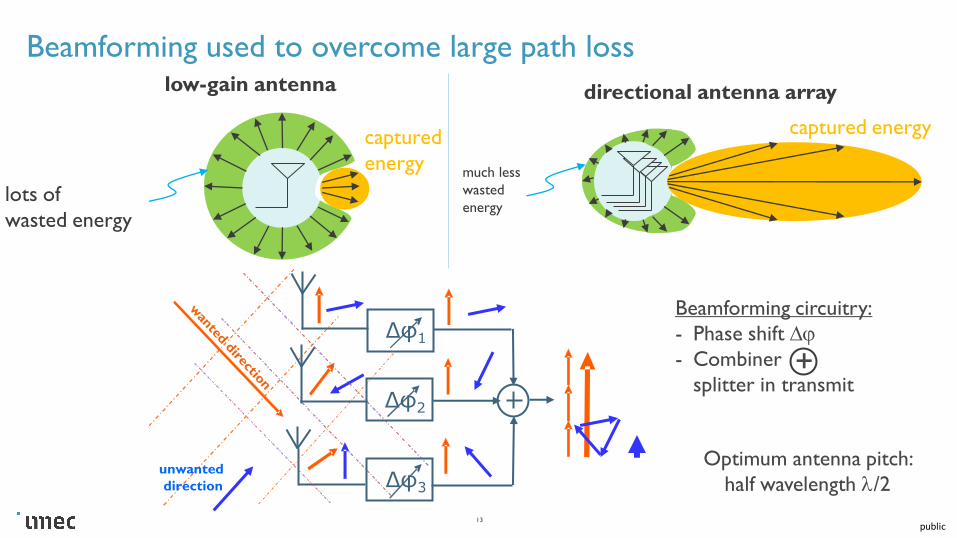
Beamforming used to overcome large path loss
13
low-gain antenna
lots of
wasted energy
captured
energy
directional antenna array
much less
wasted
energy
captured energy
Δφ3
Δφ1
Δφ2
unwanted
direction
Beamforming circuitry:
- Phase shift Dj
- Combiner
splitter in transmit+
Optimum antenna pitch:
half wavelength l/2
public
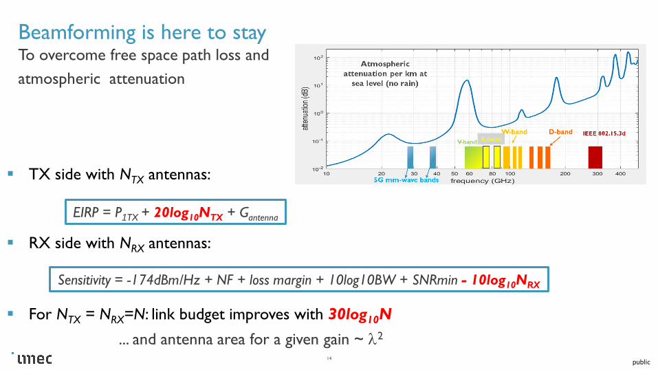
Beamforming is here to stay
▪ TX side with NTX antennas:
▪ RX side with NRX antennas:
▪ For NTX = NRX=N: link budget improves with 30log10N
14
To overcome free space path loss and
atmospheric attenuation
Sensitivity = -174dBm/Hz + NF + loss margin + 10log10BW + SNRmin - 10log10NRX
EIRP = P1TX + 20log10NTX + Gantenna
... and antenna area for a given gain ~ l2

public
Larger the antenna array → less power per power amplifier needed
15
TX power
needed (dBm)
#antennas
array size (l/2 pitch at 140GHz) [mm x mm]35x3511x113.5x3.5
public
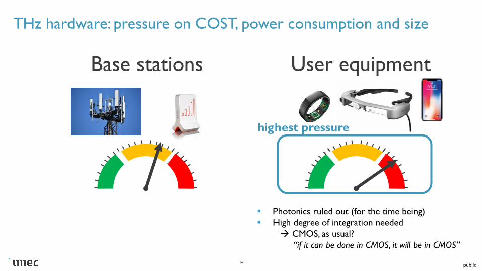
THz hardware: pressure on COST, power consumption and size
16
User equipmentBase stations
highest pressure
▪ Photonics ruled out (for the time being)
▪ High degree of integration needed
→ CMOS, as usual?
“if it can be done in CMOS, it will be in CMOS”
public
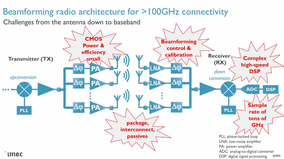
Beamforming radio architecture for >100GHz connectivity Challenges from the antenna down to baseband
Dj
Dj
Dj
upconversion
PLL
Dj
Dj
Dj
down
conversion
PLL
DSPADC
Complex
high-speed
DSP
CMOS
Power &
efficiency
small
Beamforming
control &
calibration
Sample
rate of
tens of
GHzpackage,
interconnect,
passives
Transmitter (TX)Receiver
(RX)
PA
PA
PA LNA
LNA
LNA
PLL: phase-locked loop
LNA: low-noise amplifier
PA: power amplifier
ADC: analog-to-digital converter
DSP: digital signal processing

public
The BIG challenge: power generation above 100 GHz
19
InP PAs: higher power + higher efficiency
<10%<10%
<10% <20..30%
CMOS SiGe
InPGaAs
From H. Wang et al. , “Power Amplifiers Performance Survey 2000-Present," [Online]. Available: https://gems.ece.gatech.edu/PA_survey.html
public
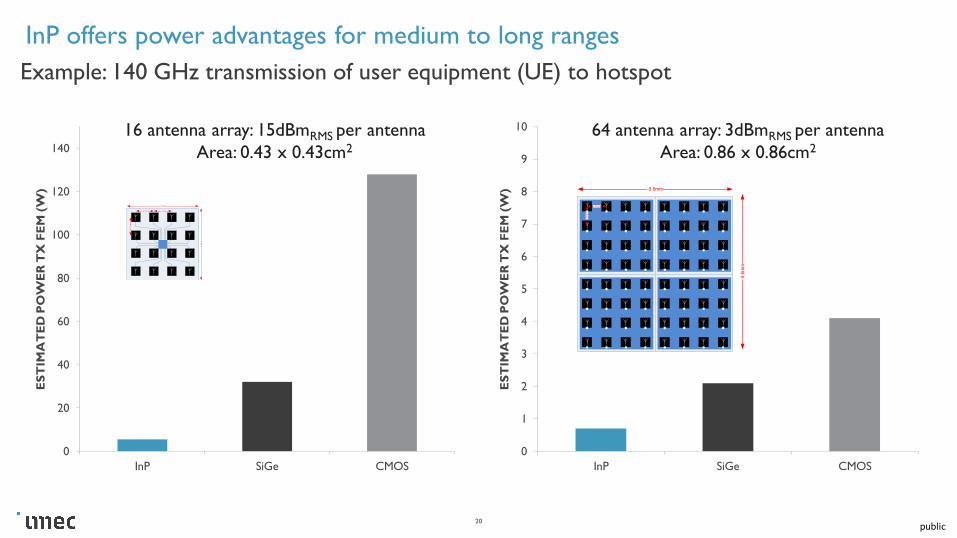
InP offers power advantages for medium to long ranges
0
20
40
60
80
100
120
140
InP SiGe CMOS
ES
TIM
AT
ED
PO
WE
R T
X F
EM
(W
)
20
Example: 140 GHz transmission of user equipment (UE) to hotspot
0
1
2
3
4
5
6
7
8
9
10
InP SiGe CMOS
ES
TIM
AT
ED
PO
WE
R T
X F
EM
(W
) 8.6mm
1.07mm
1.0
7m
m
8.6
mm
4.3mm
4.3
mm
1.07mm
1.0
7m
m
λ/2
16 antenna array: 15dBmRMS per antenna
Area: 0.43 x 0.43cm2
64 antenna array: 3dBmRMS per antenna
Area: 0.86 x 0.86cm2

public
INP ADVANTAGE REMAINS WHEN BASEBAND IS INCLUDED▪ Scenario of transmission from UE to hotspot, 32 antennas in UE (9dBrms)
▪ Power estimates with digital downscaled to 2nm
▪ assuming power reduction of 35% per new logic generation
▪ Total power consumption heavily PA-dominated
21
Link (Tx+Rx) efficiency: factor 2.5 difference between full CMOS and CMOS + InP
Grows with frequency, distance and smaller form factor.
RXTX
CMOS: 0.81 nJ/bit
0
20
5
15
10
Po
wer
[W]
0
20
5
15
10
Po
wer
[W] InP: 0.33 nJ/bit
TX RX

public
GaN: a game changer above 100 GHz?
22
Mobility similar to Si but much wider bandgap...
Cwiklinski et al., T-MTT 2019
4-stage PA, 107-148 GHz
100nm GaN on SiC,
fT/fMAX = 100/300 GHz
VDD = 15V, Gain > 25 dB
Pout = 26.4 dBm, PAEmax = 16.5%

public
Is InP ready for the mass market?
23
Today it is a niche process...
silicon
III-V
public
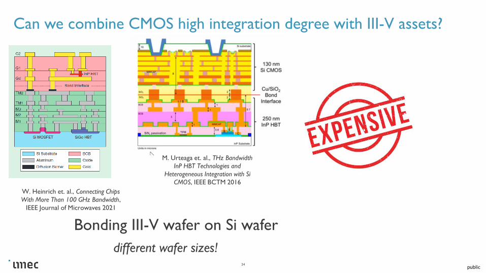
Can we combine CMOS high integration degree with III-V assets?
24
M. Urteaga et. al., THz Bandwidth
InP HBT Technologies and
Heterogeneous Integration with Si
CMOS, IEEE BCTM 2016
W. Heinrich et. al., Connecting Chips
With More Than 100 GHz Bandwidth,
IEEE Journal of Microwaves 2021
Bonding III-V wafer on Si wafer
different wafer sizes!
public
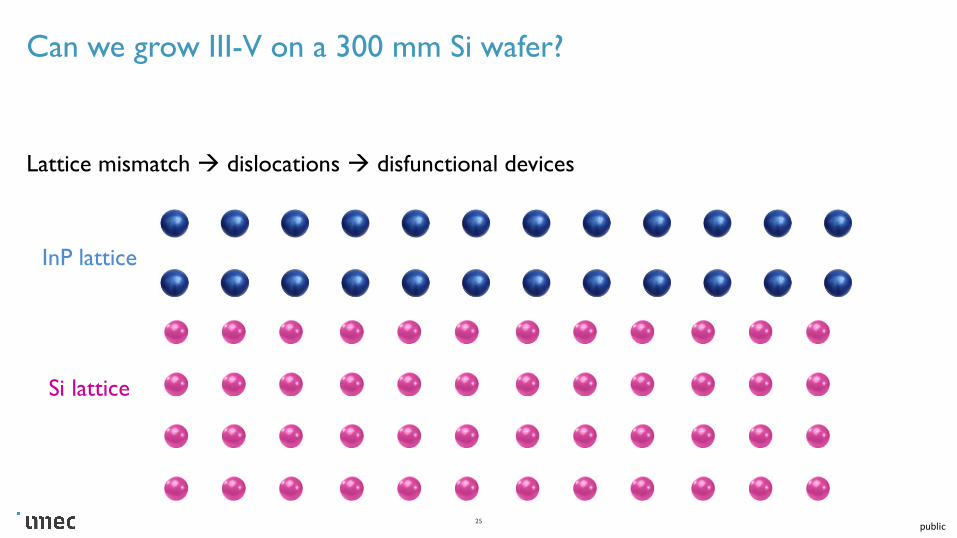
Can we grow III-V on a 300 mm Si wafer?
Lattice mismatch → dislocations → disfunctional devices
25
Si lattice
InP lattice
public
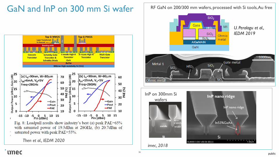
GaN and InP on 300 mm Si wafer
26
Then et al., IEDM 2020
U. Peralagu et al.,
IEDM 2019
RF GaN on 200/300 mm wafers, processed with Si tools, Au free
Si
imec, 2018
InP on 300mm Si
wafers
public
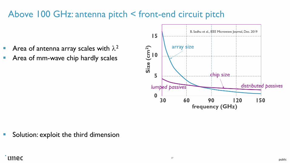
Above 100 GHz: antenna pitch < front-end circuit pitch
▪ Area of antenna array scales with l2
▪ Area of mm-wave chip hardly scales
▪ Solution: exploit the third dimension
27
public
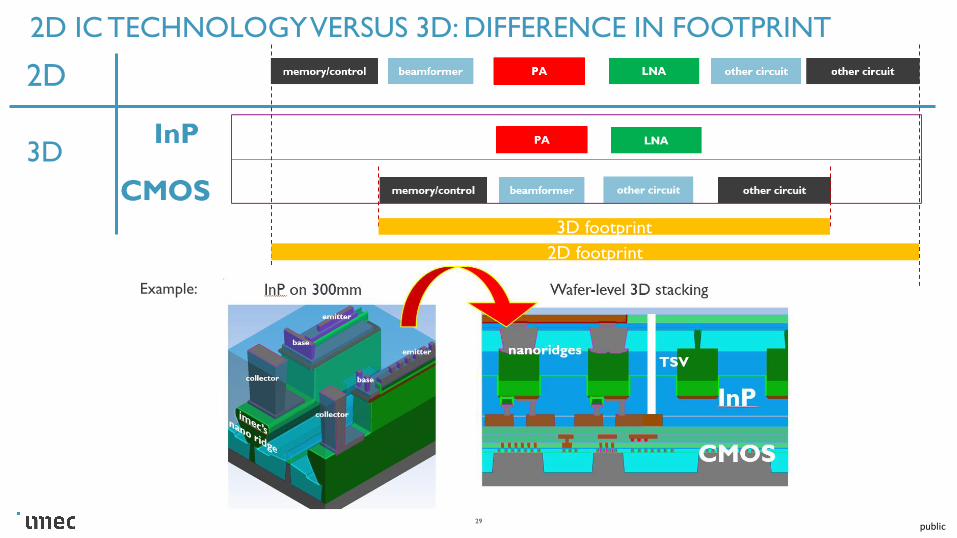
2D
29
3D
2D IC TECHNOLOGY VERSUS 3D: DIFFERENCE IN FOOTPRINT
3D footprint
2D footprint
Example:
public
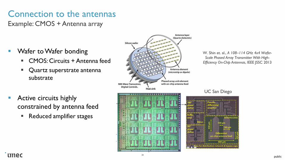
Connection to the antennas
▪ Wafer to Wafer bonding
▪ CMOS: Circuits + Antenna feed
▪ Quartz superstrate antenna
substrate
▪ Active circuits highly
constrained by antenna feed
▪ Reduced amplifier stages
30
Example: CMOS + Antenna array
W. Shin et. al., A 108–114 GHz 4x4 Wafer-
Scale Phased Array Transmitter With High-
Efficiency On-Chip Antennas, IEEE JSSC 2013
UC San Diego

public
Packaging design with heat sinks
▪ Metal Embedded Chip Assembly (MECA)
▪ Embedding different chips in a copper carrier▪ Wirebond interconnects between different chips
▪ Bandwidth issues: wirebonds
31
J. A. Estrada et. al., Metal-Embedded Chip
Assembly Processing for Enhanced RF
Circuit Performance, IEEE TMTT 2019
HRL LABORATORIES, USA
K. Nosaeva et. al., Multifinger Indium Phosphide Double-Heterostructure
Transistor Circuit Technology With Integrated Diamond Heat Sink Layer,
IEEE Trans. El. Devices 2016
▪ Thin-film Amorphous diamond heat sink layer connected to HBT device using vias▪ Best thermal material
▪ Cost may be high
▪ Power amplifier at 90 GHz▪ Pout: 20 dBm, PAE: 22 %
Ferdinand Braun Institute, Berlin

public
Conclusions
▪ The lower part of the THz gap can be filled with a full electronic approach▪ IC technologies provide a cheaper path to products than optical approaches
▪ 6G convergence of communication and sensing▪ sensing with communication hardware is feasible
▪ Low-cost D-band transceivers for user equipment: CMOS + III-V most energy efficient▪ Cost effective processing technologies being explored
▪ Packaging strategy challenged by half-wavelength antenna pitch and by heat removal strategy
▪ Non-addressed challenges: testability, EDA tools for co-design of electrical, thermal, package, IC, antenna
32


![Phase-matched scalable THz generation in two-color ... THz 10 THz 100 THz 1 PHz 10 PHz 300 m 30 m ... Kim presentation at Argonne 2012_no backup.ppt [Compatibility Mode] Author:](https://cdn.vdocuments.us/doc/165x107/5ac2b9eb7f8b9aca388e95a7/phase-matched-scalable-thz-generation-in-two-color-thz-10-thz-100-thz-1-phz.jpg)


