
Architectural choices & design-implementation methodologies for exploiting extended FD-SOI DVFS & body-bias capabilities
David JACQUET
Senior Principal Engineer CPU & GPU subsystems Technology R&D STMicroelectronics

2
2
Outline
• How to increase the energy efficiency of SOCs & CPUs ?
• UTBB FD-SOI
• Total power and body biasing
• FD-SOI and multiprocessing
• Conclusion

How to increase the energy efficiency of SOCs & CPUs ?

4
4
Dynamic power reduction : from clock switching to DVFS
DVFS
Hw component
Power Gating
Hw component
Bias
Retention mode
f=0 Hz
static power reduction :
Switch
A) Clock Switching
B) Frequency Scaling
HW Component
HW Component
HW Component
Optional Monitor
HW Component
HW Component
C) Dynamic Voltage Frequency Scaling DVFS
Operating Point
Operating Point
Idle

5 Increasing the Energy Efficiency of a SOC Architecture
Energy efficiency & Complexity
Single & fixed voltage domain SOC
Full DVFS SOC (V,F) points based on use cases
- Design can remain synchronous - Split array/periphery memories
might be needed for wide DVFS voltage range
Power domain split based on use cases
- Design can remain synchronous between power domains - Low power description flow
Single DVFS domain + power domains
Several DVFS domains + power domains
- Design can remain synchronous between power domains - Low power description flow
- Design can remain synchronous between power domains
- Design must be asynchronous between the voltage domains
- Low power description flow
3 voltage domains
9 power domains
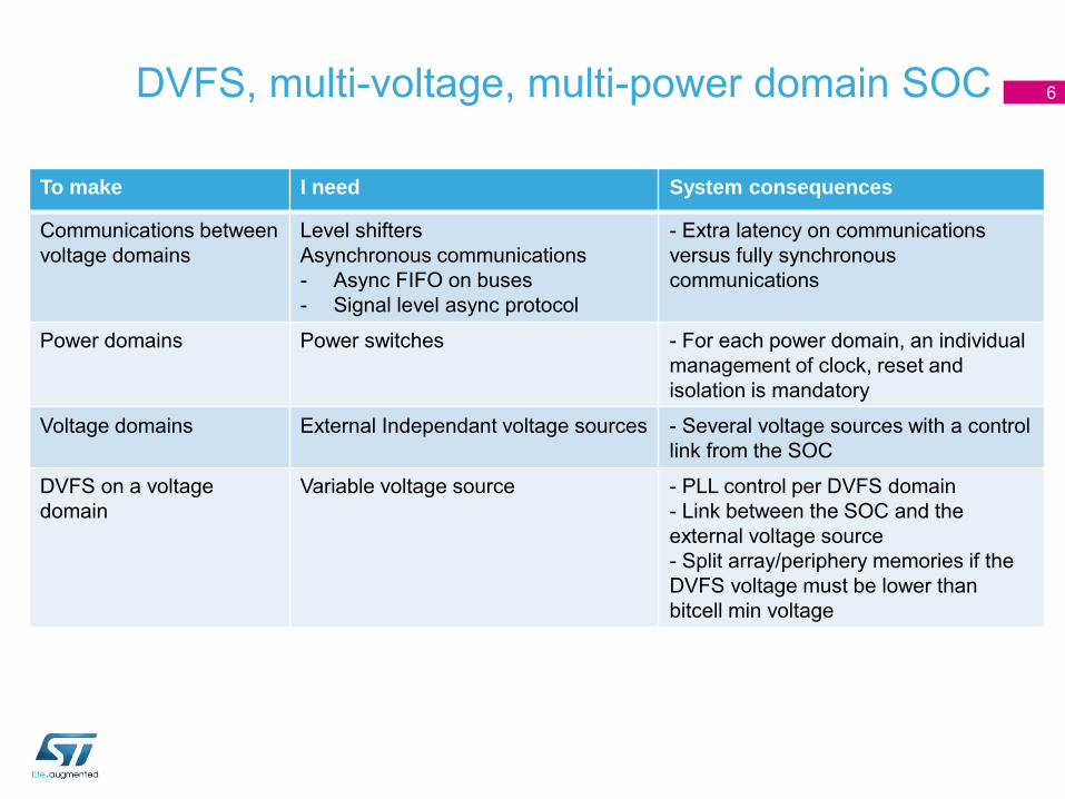
6 DVFS, multi-voltage, multi-power domain SOC
To make I need System consequences
Communications between voltage domains
Level shifters Asynchronous communications - Async FIFO on buses - Signal level async protocol
- Extra latency on communications versus fully synchronous communications
Power domains Power switches - For each power domain, an individual management of clock, reset and isolation is mandatory
Voltage domains External Independant voltage sources - Several voltage sources with a control link from the SOC
DVFS on a voltage domain
Variable voltage source - PLL control per DVFS domain - Link between the SOC and the external voltage source - Split array/periphery memories if the DVFS voltage must be lower than bitcell min voltage

7
How to increase the energy efficiency of computing systems ?
• Several techniques exists but bulk process limits their efficiency at advanced process nodes (28/14 nm)
• A new process & design techniques are needed
Technique Limitations in Bulk
Increasing the # of processing
cores
• leakage current for a given performance • see “Wide range DVFS limitations”
Poly biasing of the transistors • limited gate length modulation range
Wide range DVFS
• [Vmin, Vmax] range is limited by variability • Huge performance degradation when supply V reduces • dual rail memories limited Array/periphery voltage gap • Memory Array minimum voltage
Dynamic transistor Vt control • limited body bias range (-300 mV, +300 mV) • limited benefit in 28 nm & almost no benefit in 20/14 nm
D.Jacquet et al., VLSI Symposium 2013

UTBB FD-SOI

9 28nm Planar UTBB FD-SOI: Advantages
• Ultra-thin body
• Better SCE immunity
• Ultra-thin BOX
• Extended body biasing
• Total dielectric isolation
• Latch up immunity
• No channel doping
• Improved variability
Body-Bias
Hybrid zone
24nm
UTBB FD-SOI enables
shorter channel length
D.Jacquet et al., VLSI Symposium 2013

10
-3V
UTBB FD-SOI: Extended Body Voltage Range
• Flip Well for full forward body-bias operation
n-Well p-Well
NMOS PMOS VBN VBP noBB
FBB RBB
3V
-300mV
Unique feature for dynamic speed/leakage optimization
D.Jacquet et al., VLSI Symposium 2013

The total power & body biasing

12 Energy Efficiency and Leakage • In any technology node, a tradeoff must be made between speed and leakage
• At a given voltage • The maximum speed can be increased at the expense of higher leakage
• Or for a given maximum speed • The minimum voltage to reach this performance can be reduced at the
expense of higher leakage • The lower the supply voltage, the lower the dynamic power (in ~V2)
• At the end, what counts is the “total power”=leakage+dynamic power
• In FD-SOI, the wide Body-Bias range allows this tradeoff to be dynamically optimized to the conditions
• Process conditions • Temperature conditions

Total power graph example – 28nm FD-SOI 13
“Total power” vs performance (body biasing & DVFS)

Dual ARM A9 in 28nm FD-SOI

15 Dual ARM A9 subsystem architecture
Soc supply
Vana
AXI FIFO AXI FIFO
misc i/f misc i/f
ls
ctrl regs
AXI
SCU/L2 cache logic
cache memories periphery
L2 cache + L2 tag memories array
CPU Core #0 logic
CPU Core #1 logic
6T ram arrays
L1 ram periph
6T ram arrays
L1 ram periph
body biased region under Varm
vbbn/ vbbp
Body-Bias generator
DVFS ctrl
Process Monitors
Varm
on-die decap
Vmem
clamp
on/off switch
on/off switch
power switch
power switch
power switch
PLL
D.Jacquet et al., VLSI Symposium 2013

Body-Bias voltage generation • How to generate programmable body voltages ?
16
gnds grid
PW
P
W
NM
O
S
PM
O
S
D-N
W
P-S
UB
NW
vdds grid
FBB : positive V 0V
t
FBB : negative V 0V
t
DAC
0 -1.3V
Neg. Charge Pump
1V8
GND
-1V8
DAC
0 1.3V
D.Jacquet et al., VLSI Symposium 2013

Fully digital testing of the BBgen 17
Body Bias Gen
vbbn
vbbp
Process monitor
Process monitor
Process monitor frequency (MHz)
Volt
age (
V)
Slide 17
Tester digital interface
• The BBgen is generating 2 independent voltages • For the Nmos [0 to 1.3V] & Pmos [-1.3V to 0V] bodies • With a resolution of 100 mV • The embedded process monitors allow a full digital test of the BBGen in
production test • No need for body nodes external access • Full access via a digital interface
D.Jacquet et al., VLSI Symposium 2013

Only few mV
1ms
Fast dynamic body-bias management
• Low Zout amplifiers allow ms settling time of the body nodes
• E.g. 3 body domains connected to the same generator • Each body domain can be activated
• In less than 1ms • Activating any body domain does not disturb the voltage of the others
18
BB Domain#2 voltage
BB Domain#1 voltage
BB Domain#0 voltage
Slide 18 D.Jacquet et al., VLSI Symposium 2013

Body-Bias voltage grid 19
• A very thin [X,Y] grid is routed over the body-biased region
• No static current has to be provided • The current is limited to “C.dV/dt” during the body-bias transitions
gnds vdds
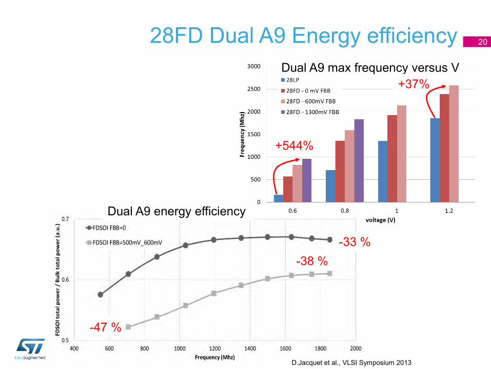
28FD Dual A9 Energy efficiency 20
Slide 20
Dual A9 max frequency versus V
Dual A9 energy efficiency
+544%
+37%
-33 % -38 %
-47 %
D.Jacquet et al., VLSI Symposium 2013

Continuous & wide DVFS • 0.5V to 1.4V DVFS range
• Continuous functionality in this voltage range
21
Slide 21
3.0 GHz at 1.37V
2.3 GHz at 1.0V
1000 MHz at 0.61V
300 MHz at 0.5V
CP
U fr
eque
ncy
(MH
z)
CPU supply (V) 0.5 0.6 0.7 0.8 0.9 1.0 1.1 1.2 1.3 1.4
3000 MHz
2000 MHz
1000 MHz
D.Jacquet et al., VLSI Symposium 2013

FD-SOI & multiprocessing

23
23
Multicore Delivers more MIPS/mW • No doubt multicore can deliver more MIPS per mW
• Core should be implemented for best power efficiency/peak frequency trade-off
• SoC should host as many cores as possible at every technology node • scalability achieved through core number increase • no more by frequency scaling
• Major issues • Amdahl’s law • Memory hierarchy efficiency
D.Jacquet et al., VLSI Symposium 2013

24
24
Multiprocessing and wide DVFS - 1 • FD-SOI provides more performance at same voltage as bulk
• Also a much lower performance degradation when lowering the supply voltage (dperf/dV)
• And, as consequence, a very good efficiency on multiprocessing applications
D.Jacquet et al., VLSI Symposium 2013

25 Multiprocessing and wide DVFS - 2
• 2 cores vs 4 cores • Ideal speed up factor • 2 cores@F=4 cores@F/2
Dyn power gain ~41%
Dyn power gain ~64%
‘4 cores’ frequency
‘2 cores’ frequency
28FD-SOI relative performance vs V
28LP bulk relative performance vs V
fbb=0
fbb=0.5
fbb=1.2 fbb=0.8
fbb=0.2
D.Jacquet et al., VLSI Symposium 2013
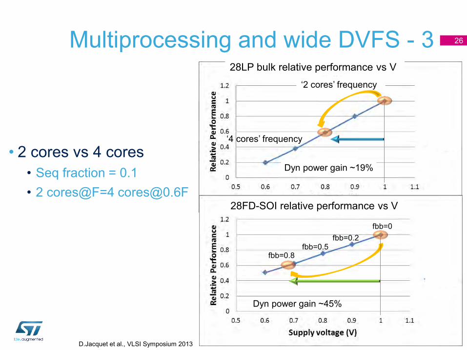
26 Multiprocessing and wide DVFS - 3
• 2 cores vs 4 cores • Seq fraction = 0.1 • 2 cores@F=4 [email protected]
Dyn power gain ~19%
Dyn power gain ~45%
‘4 cores’ frequency
‘2 cores’ frequency
28FD-SOI relative performance vs V
28LP bulk relative performance vs V
fbb=0
fbb=0.5 fbb=0.8
fbb=0.2
D.Jacquet et al., VLSI Symposium 2013

27
27
Conclusion
• We have demonstrated that FD-SOI enables dynamic management of the leakage/dynamic-power tradeoff
• The Energy Efficiency of Multiprocessing systems can be perfectly exploited thanks to FD-SOI high performance at low voltage & wide DVFS range
• A first-time silicon success Dual ARM A9 in 28nm UTBB FD-SOI demonstrates
• CPUs running from 300 [email protected] to 3000 Mhz in continuous DVFS • Fully integrated
• Body-Bias generator • Advanced IPs for power management

Thank You
28


