AN INDUCTION MOTOR DRIVE USING A RESONANT DC LINK INVERTER
Thesis
Submitted To
Graduate Engineering & Research School of Engineering
UNIVERSITY OF DAYTON
In Partial Fulfillment of the Requirements for
The Degree
Master of Science in Electrical Engineering
by
Gregory Louis Fronista
UNIVERSITY OF DAYTON
Dayton, Ohio
December 1995
U N IVER SITY OF DAYTON ROESCH LIBRARY

9S 07 8 7 3
AN INDUCTION MOTOR DRIVE USING A RESONANT DC LINK INVERTER
Approved by:
Malcolm W. Daniels, Ph.D. Assistant Professor Electrical Engineering Committee Chairperson
Richard J. Kee, D.E. Assistant Professor Electrical Engineering Committee Member
Tomip^ L. Williamson^ Ph.D.Associate Professor Electrical Engineering Committee Member
Donald L. Moon, Ph.D.Associate DeanGraduate Engineering Programs & Research School of Engineering
-------?-----r '—7— ----Joseph Lestingi, D.Eng.. P.E. DeanSchool of Engineering
it

ABSTRACT
AN INDUCTION MOTOR DRIVE USING A RESONANT DC LINK INVERTER
Fronista, Gregory LouisUniversity of Dayton, 1995
Advisor: Dr. Malcolm W. Daniels
New initiatives to increase the use of electrical power, such as the electric vehicle and
the More Electric Airplane, have created a need for improved motor drives. The use of
adjustable speed drives has recently received more attention in these applications because
new circuit topologies and power components have been developed that have enabled
improvements in efficiency, power density, and response times. This thesis reports the
design and simulation of an actively clamped resonant dc link inverter that will drive an
induction motor based blower. The objective of this thesis is to design, build and test a
resonant dc link (RDCL) inverter and compare the performance of a six-step control strategy
with a pulse density modulation strategy in an adjustable speed drive. Comparisons are made
between a hard switched pulse width modulation converter and an RDCL inverter.
Theoretical and experimental power loss calculations of the RDCL inverter are compared and
discussed. The performance of constant voltage/frequency adjustable speed control is
presented.
iii

TABLE OF CONTENTS
Chapter Page
1. INTRODUCTION 1
2. RESONANT DC LINK INVERTER DESIGN 7
THEORETICAL ANALYSIS OF RDCL INVERTER 7
Resonant Link Voltage and Current AnalysisLimiting the RDCL Voltage OvershootPower Loss Analysis and RDCL Design Equations
DESIGN SPECIFICATION AND PARAMETER SELECTION 16
SELECTION OF RESONANT AND CLAMP SWITCHES 17
CONTROL OF RESONANT AND CLAMP SWITCHES 19
CONTROL OF MAIN SWITCHES 21
Six-step ControlPulse Density Modulation Control
3. FABRICATION OF RDCL MOTOR DRIVE 25
DIGITAL CONTROL CIRCUITRY 25
RESONANT LINK INDUCTOR DESIGN 28
4. EXPERIMENTAL RESULTS OF RDCL MOTOR DRIVE 33
RDCL VOLTAGE AND CURRENT WAVEFORMS 33
NO-LOAD MOTOR DRIVE RESULTS 36
FULL-LOAD RDCL MOTOR DRIVE RESULTS 39
5. CONCLUSIONS 44
IV

References 47
Appendices
APPENDIX A Digital Signal Processor Programs 48
APPENDIX B Node Equations for Saber Simulations 55
APPENDIX C Resonant Inductor Characterization Curves 59
V

DEFINITIONS OF ABBREVIATIONS
HHoQCOO0AcAPBT>
CcCrFfifrf s
fs,
IIId
IIImIoklgLrMmfMLTNnsn sl
PzP cu
PDMPfeP„
Neper frequencyPermeability of magnetic corePermeability of airResistance correction factorFrequency (rad/sec)Resonant frequency (rad/sec)Area of magnetic coreArea productFlux densityMaximum flux densityClamp capacitorResonant capacitorFringing flux factorSwitching frequency of sine wave for PDM Resonant frequency (Hz)Switching frequency of triangle wave for PDMSlip frequencyInverter bus reversal currentInverter currentResonant inductor currentInitial resonant inductor currentOutput currentClamp voltage constantAir gap of magnetic coreResonant inductorSpeed control constantFrequency modulation ratioMean length turnNumber of turnsSynchronous speedSlip speedTotal power loss of magnetic coreCopper power loss of magnetic core Pulse density modulation Ferrite power loss of magnetic core Gap power loss of magnetic core
vi

PcPWMQRDCLRwSTtfTHDV/fVdV*,VLVsA
Output powerPulse width modulation Quality factor Resonant dc link Linear resistance of wire Apparent power TorqueFall-time for power switch Total harmonic distortion Voltage over frequency ratio Resonant voltage Forward drop of power switch Inductor voltage Source voltageImpedance of resonant tank circuit
vii
CHAPTER 1
INTRODUCTION
Power conversion is required to effectively and efficiently control motors of all kind.
Performance of the overall system is greatly dependent on the appropriate conversion and
control of power to the motor. For example, a system could utilize the most efficient motor
and still operate very inefficiently if the motor is not driven properly. Significant
improvements can be made in the efficiency, power density and reliability of present motor
drives by using new topologies that take advantage of the new switching devices available.
These topologies operate at higher switching speeds and employ new control strategies that
lead to their increase in performance. These motor drives are required for a new initiative
within the Air Force titled the More-Electric Aircraft (MEA).
The MEA's goal is to reduce or eliminate all non-electrical lines such as hydraulic,
pneumatic and bleed air and replace them with electrical lines. Therefore, the power
electronics must be reduced in size and weight and have better fault tolerant performance.
One place that a high efficiency, quick responding motor drive will be needed is in the area
of actuator drives. These devices could range from fractional horsepower to 100s of
horsepower. New motor drives are required to make the MEA feasible.

2
Conventional motor drives (Fig 1.1) operate in a hard-switched mode that increases
losses and generates tremendous device stresses. The stresses placed on these devices also
reduce the reliability of these motor drives. The majority of these motor drives require large
snubber circuits for the switching devices to limit the voltage and current transients that
could destroy the devices. These snubber circuits slow down the switching speed of these
power devices, increase losses in the circuit, and add size and weight to the motor drive. The
switching devices heat up due to the switching losses and operate less efficiently affecting
the efficiency of the entire motor drive. These factors limit the switching frequency of the
motor drive causing less than optimal efficiency.
Another desirable feature is to go to higher switching frequencies to reduce
electromagnetic interference (EMI), harmonic distortion, and greatly reduce the size and
weight of the magnetic components and capacitors. In order for higher switching frequencies
to be attainable, a great deal of time and money has been spent by various organizations to
improve the power switching devices, leading to the advent of the insulated-gate bipolar

3
transistor (IGBT) and the MOS-controlled thyristor (MCT). These devices have higher
switching speeds leading to reduced switching losses, reduced on voltage and improved safe
operating areas (SOA), however, the switching frequencies are still limited. In order to attain
higher switching frequencies, a new topology must be implemented. The concept of a soft-
switching, resonant DC link (RDCL) converter was introduced by D.M. Divan [1] to increase
the switching frequency. Efficiency is increased because switching losses are nearly
eliminated which are a large portion of the losses in a PWM inverter. Snubbers are
eliminated which increases power density. The inverter bridge devices require minimal
cooling and no longer have large voltage stresses, both contributing to improved reliability.
New control strategies also can be implemented that will allow faster response, and
yield improvements in EMI and harmonic distortion. One of the latest control strategies
implemented in power conversion is called pulse density modulation (PDM). This is similar
to pulse width modulation where a sine wave is emulated using a series of pulses. When a
reference sine wave is at its maximum, the density of pulses is high, and when the sine wave
is at its minimum, there are few pulses. This strategy is shown in Fig. 1.2.
Figure 1.2 - Pulse density modulation waveforms

4
A resonant DC link (RDCL) inverter is illustrated in Fig. 1.3. This topology involves
placing a simple L-C resonant circuit between the DC bus and a conventional inverter. The
RDCL operates in the following manner. A DC voltage (Vs) is applied to a parallel L-C
Resonant Voltage Output
Figure 1.3 - Basic resonant DC link circuit
resonant circuit with a switch Sr across the capacitor. By closing Sr , the inductor L r is
charged. When Lr is charged to a sufficient level, Sr is opened and the resonant bus voltage
oscillates and returns to zero. A Saber™ simulation of this operation is shown in Fig. 1.4
where Vd is the RDCL bus voltage and I L is the resonant inductor current. The resonant
Figure 1.4 - Resonant voltage and current waveforms
5
switch is closed every time the resonant bus voltage returns to zero. At this time, the power
switching devices in the inverter bridge are turned on or off ensuring a zero voltage
transition. The idea is simple, however, until recently, technological restrictions limited the
practical realization of the topology. The topology is subject to three main limitations;
voltage overshoots, zero crossing failure and resonant circuit losses.
Ideally the RDCL bus voltage will ring up to approximately 2 Vs and then return to
zero. When the motor is loaded, the voltage could overshoot as high as 3 Vs when the load
current goes from its maximum to minimum current. This large voltage overshoot problem
can be solved with passive or active clamping [2]. When using passive or active clamping,
zero crossing failures can be eliminated by appropriate control of the resonant switch. The
most recent control strategy proposed involves sensing the RDCL inductor current, and using
a current initialization scheme to set the inductor current to the appropriate value depending
on the inverter current [Bose, 3], By accomplishing this both link voltage overshoot and zero
crossing failures are avoided. If this voltage is not assured to return to zero, possibly from
high parasitic resistances in the resonant inductor and capacitor, Sr will draw a large current
from the capacitor that could destroy the switching device.
Combining soft-switching with PDM yields a motor drive that has improved
performance when compared with conventional motor drives. These advantages are attained
because all switching occurs at either zero voltage or zero current, thus making switching
losses in the power conversion hardware negligible and allowing the switching devices to
operate at the extreme (Fig. 1.5) of their safe operating areas (SOA).
6
Figure 1.5 - Comparison of safe operating area for a power device in RDCL and PWM inverter
In practice only parts with a high Q-factor (low equivalent series resistance) may be
used. These components must operate at a resonant frequency in the range of 20-200 kHz
for power circuits, and have very high quality factors. The resonant inductor is the
significant component because if there is a large equivalent series resistance involved, then
the DC bus will not return to zero while keeping the peak voltage at a reasonable level. A
quality factor of 100+ is typically required for the inductor to keep losses low.
This thesis reports the design and simulation of an actively clamped resonant dc link
(ACRDCL) inverter that will drive an induction motor - blower. The objective of this thesis
is to design, build and test an RDCL inverter and compare the performance of a six-step
control strategy with a PDM strategy in an adjustable speed drive. Comparisons will be
made between a hard switched PWM converter and an RDCL inverter. Theoretical and
experimental power loss calculations of the RDCL inverter will be compared and discussed.
The performance of constant voltage/frequency ratio adjustable open-loop speed control will
also be presented.

CHAPTER 2
RESONANT DC LINK INVERTER DESIGN
This chapter presents the theoretical analysis and simulation modeling of the resonant
DC link inverter design. The design synthesizes information from both theoretical and
numerical analysis to obtain component values for experimental implementation of the
circuit.
2.1 THEORETICAL ANALYSIS OF RDCL INVERTER
A theoretical analysis of the RDCL inverter enables the selection of critical
components and prediction of the power losses of each component. This reveals where
improvements in components can bring about the biggest performance gains. The theoretical
analysis will be compared with the experimental results and if any large discrepancies exist,
action can be taken to optimize the circuit and eliminate as many parasitic losses as possible.
The theoretical analysis also provides information pertaining to heat sink requirements if they
are necessary for the various power components.
2.1.1 RESONANT LINK VOLTAGE AND CURRENT ANALYSIS
The equivalent circuit of the RDCL during each resonant cycle can be seen in Fig.
2.1. Throughout the remainder of this text, the IGBT and associated free-wheeling diode will
be shown schematically as an ideal switch for simplicity. To simplify the analysis for this
7
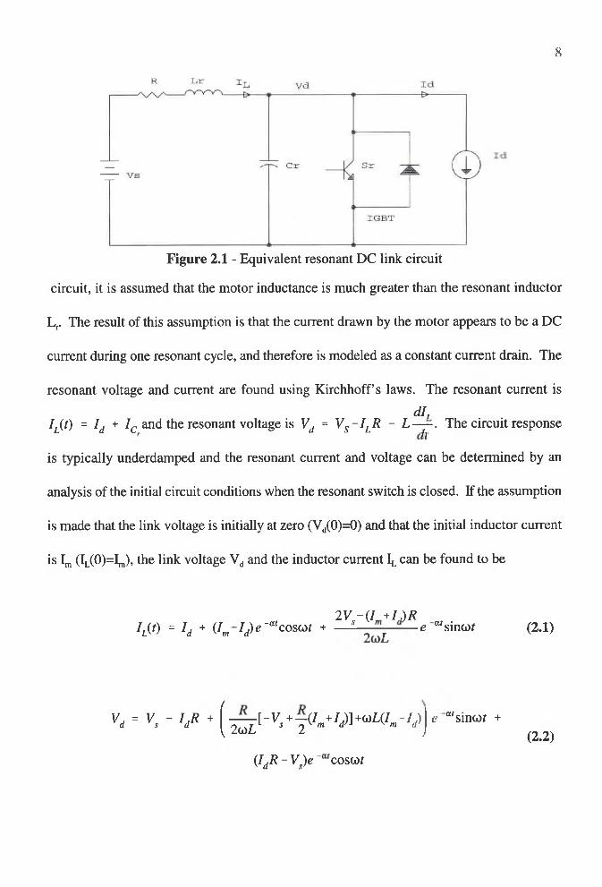
s
Figure 2.1 - Equivalent resonant DC link circuit
circuit, it is assumed that the motor inductance is much greater than the resonant inductor
Lr. The result of this assumption is that the current drawn by the motor appears to be a DC
current during one resonant cycle, and therefore is modeled as a constant current drain. The
resonant voltage and current are found using Kirchhoff’s laws. The resonant current is
di,IL(t) = Id + Ic and the resonant voltage is Vd = VS~ILR - L —j~- The circuit response
is typically underdamped and the resonant current and voltage can be determined by an
analysis of the initial circuit conditions when the resonant switch is closed. If the assumption
is made that the link voltage is initially at zero (Vd(0)=0) and that the initial inductor current
is Ih, (IL(O)=Im), the link voltage Vd and the inductor current IL can be found to be
2 V - ( / + / . ) / ?4,(0 = 4 + ( 4 - 4 ) e ' “' coswr + \ r e “'sincof (2.1)
V' = V - I .R + f — [ - V + - ( / + / . ) ] + o L ( / - Z J I f r a's in o t + d s d { 2 a L 5 2 m d m d ) (2.2)
(IdR - Vs)e cosot

9
where the constants a , to and to0 ar given by
a2L (2.3)
M e
L -> o = \ to - aA o
(2.5)
(2.4)
These equations are valid until Vd returns to zero, when the free-wheeling diode in the switch
conducts and clamps Vd to zero. At this time, the switch S ris turned on again and the current
in the inductor is reinitialized to the value, 1̂ ,.
If the parasitic inductor resistance R, is required to be as small as possible to
maximize efficiency, we can assume that R « toL. Using these assumptions, equations 2.1
and 2.2 reduce to
“'sintot (2.6)
V /0 = v s + wL(/m- / d) e “'sintor - Vse “'costof (2.7)
It can be seen in equation 2.7 that the link voltage Vd is dependent on the term (!„, - 1,,). If
this term is monitored, the link voltage can be regulated to guarantee that its peak voltage is
approximately 2VS This also ensures that the link voltage returns to zero. This enables all
of the inverter switches to be turned on or off with no switching losses.
2.1.2 LIMITING THE RDCL VOLTAGE OVERSHOOT
The RDCL inductor current can be initialized to the proper level only when Id does
not change much or when it increases. This is accomplished by keeping the switch closed
10
long enough so the current increases to the appropriate level. When Id experiences a sudden
decrease however, the current through the inductor must be reduced. This cannot be
accomplished with the basic RDCL circuit. If this current is not decreased, the link voltage
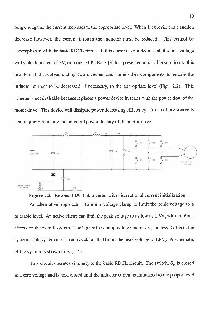
will spike to a level of 3VS or more. B.K. Bose [3] has presented a possible solution to this
problem that involves adding two switches and some other components to enable the
inductor current to be decreased, if necessary, to the appropriate level (Fig. 2.2). This
scheme is not desirable because it places a power device in series with the power flow of the
motor drive. This device will dissipate power decreasing efficiency. An auxiliary source is
also required reducing the potential power density of the motor drive.
Figure 2.2 - Resonant DC link inverter with bidirectional current initialization
An alternative approach is to use a voltage clamp to limit the peak voltage to a
tolerable level. An active clamp can limit the peak voltage to as low as 1.3VS with minimal
effects on the overall system. The higher the clamp voltage increases, the less it affects the
system. This system uses an active clamp that limits the peak voltage to 1.8VS. A schematic
of the system is shown in Fig. 2.3.
This circuit operates similarly to the basic RDCL circuit. The switch, Sr, is closed
at a zero voltage and is held closed until the inductor current is initialized to the proper level

11
Figure 2.3 - Actively clamped resonant DC link inverter
to assure that the link voltage returns to zero with a minimum peak voltage. When the link
voltage reaches the proscribed clamp voltage, kVs = 1.8VS in this case, the clamping switch
Sc, will turn on to limit the link voltage. The clamp switch will remain closed until the net
charge transferred into the clamp capacitor is zero, which will maintain the clamp voltage
at kVs. The clamp switch is opened at the appropriate time and the link voltage returns to
zero whence the process repeats itself. Typical resonant voltage and resonant and clamp
Figure 2.4 - Resonant voltage and timing diagrams for gate signals
12
switch gate controls are shown in Fig. 2.4.
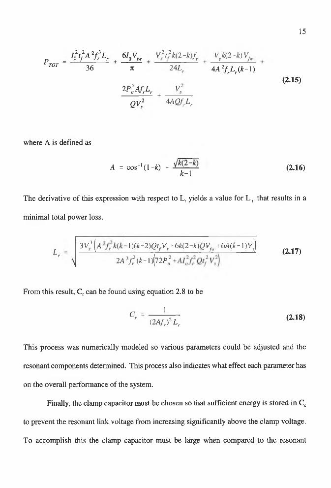
To simplify the analysis of the circuit, the equivalent circuit in Fig. 2.5 is used,
similar to the approach used earlier to determine the inductor current IL and link voltage Vd.
The resonant frequency (fr) of the system has been shown [4] to be
fr =1
/------------'I2JL~Cr cos’l l - Jfc) + vfc(2 ~ ®
V r r { k - 1 )(2.8)
Figure 2.5 - Equivalent actively clamped resonant DC link inverter
2.1.3 POWER LOSS ANALYSIS AND RDCL DESIGN EQUATIONS
In order to select an inductor and capacitor for the resonant link, the power loss of
each component is found, and the inductor chosen to minimize the power loss. Three types
of power losses are considered in this assessment; switching losses in the RDCL and inverter
switches, conduction losses in both the RDCL and inverter switches, and i2R losses in the

13
resonant link inductor. Since all the switching will be performed very close to zero volts, the
switching losses should be small. The following power loss equations were derived by T.M.
Jahns, et al. [4]. Assuming that a pulse density modulation (PDM) strategy is adopted, the
switching loss in the main inverter switches is,
Psm
I 2 t 2j o144 C
(2.9)A
Assuming that all of the devices have equal forward drops (Vfw) for all the main
inverter switches, the corresponding conduction losses can be shown to be
Pcm 7t(2.10)
To determine the switching losses of the clamp device a linear current fall turn-off
model is used. It is assumed that the switch is turned off when the inductor current reaches
the minimal level necessary to ensure that the link voltage returns to zero. The switching
losses in this case are characterized as,
V 2 2 ,k(2 - k)P ------------ f
sc 24 L(2.11)
The conduction loss of the clamp device is expressed assuming that the forward drop of the
switch is and the conduction losses are the same in the switch and the antiparallel diode
P =Vsk{2 - k)VfwC
L f r (2.12)k - 1

14
The losses in the resonant components depend greatly on the quality of the components used
to implement the resonant link. There are many high quality capacitors available “off the
shelf’ made of polypropylene, polystyrene or even ceramics, that offer low equivalent series
resistance (ESR) ratings. Therefore, the losses of the resonant circuit are dominated by the
resonant inductor. The inductor must handle not only the DC current that is being drawn by
the motor but also the high frequency resonant current generated by the resonant link itself.
Assuming a constant quality factor Q for the resonant inductor, the losses in the resonant
circuit can be approximated by
P = —r ESR q 2QZr(2.13)
where
(2.14)
and Po is the output power.
By summing all of the above power losses, the total power loss can be found.
Substituting equation 2.14 into the total power loss equation and eliminating Cr using
equation 2.8, the resulting equation for the total power loss is expressed as a function of Lr
and other known system variables.
15
n _ l ^ A ^ r Lr 6IoVfiv V 2t 2k (2 -k )fr ‘ tot 36 Tl 24L
v sM - V v fw
4 A 2f rL r(k - l)
where A is defined as
2P2oAfrLr + v; GV2 + ^ Q fP r
(2.15)
A = c o s - '( l - t ) *k - i
(2.16)
The derivative of this expression with respect to Lr yields a value for L r that results in a
minimal total power loss.
L rN
3 V3 (a l)(^-2)gzz.vr + 6 ^ ( 2 - ^ ^ , + 6/1^ - l ) v j
2A y r2( ^ - 1 )(72P,7(2.17)
From this result, Cr can be found using equation 2.8 to be
1( 2 < ) % (2.18)
This process was numerically modeled so various parameters could be adjusted and the
resonant components determined. This process also indicates what effect each parameter has
on the overall performance of the system.
Finally, the clamp capacitor must be chosen so that sufficient energy is stored in Cc
to prevent the resonant link voltage from increasing significantly above the clamp voltage.
To accomplish this the clamp capacitor must be large when compared to the resonant

16
capacitor. To size this capacitor, Cc must be selected to limit AVc1, the excess clamp voltage,
to prevent damage to the inverter switches. The clamp capacitor voltage increase is
expressed [4] as,
/
(£ -l)V ?2 +C
(2.19)
\
where I , is the inverter bus reversal current.
2.2 DESIGN SPECIFICATION AND PARAMETER SELECTION
The following design parameters are adopted for the analysis:
Vs Source voltage 270 vdctf Fall-time for main switch 1 psIo Output current 18.5 Ak Clamp voltage constant 1.8Q Quality factor of resonant components 200f, Resonant frequency 45 kHz
For these parameters, the resonant inductor Lr is found using equation 2.17 to be 39.8 pH,
and the resonant capacitor is found to be 309 nF using equation 2.18. The capacitor chosen
was a 330 nF capacitor made by Philips with an esr of 10 mQ. The required inductor is
custom fabricated. The switches are selected more easily after the circuit is simulated to
determine maximum voltage and current levels required for the design.
The value for the clamp capacitor is found using the results above and inserting
them into equation 2.19. Further parameters need to be defined to make this determination.
Assuming that i, = 75 A and that AVcl should be limited to less than 50 V, a capacitor value
of 10 pF is sufficient. The maximum voltage in this case is 536 V, sufficiently less than the

17
inverter switch voltage rating of 600 V.
The selected RDCL components are simulated in Saber™ to verify the circuit’s
performance. These simulations also aid in the selection of the switching devices in the
RDCL and the inverter.
2.3 SELECTION OF RESONANT AND CLAMP SWITCHES
Although the resonant components were designed to handle a 5 kW load, the circuit
simulation is based on the induction motor-based blower motor that will be used in the
Figure 2.6 - Resonant switch current when Vd is switched at 30 V
experimental portion of this thesis. This motor is a three-phase Y-connected induction motor
with a nameplate rating of 220 V, 1.8 A. The load is modeled as a constant current sink for
the simulation with a peak amplitude of 2.5 A. The schematic for the equivalent circuit is
shown in Fig. 2.5. The simulation showed a peak resonant switch current of 10.5 A. This
current can vary tremendously because Sr shorts out the resonant capacitor. Since the current
through a capacitor is approximately i = C — , it is evident that even if the voltage is dt
slightly positive or negative a significant amount of current can be pulled from the capacitor.
18
r -4
1 I
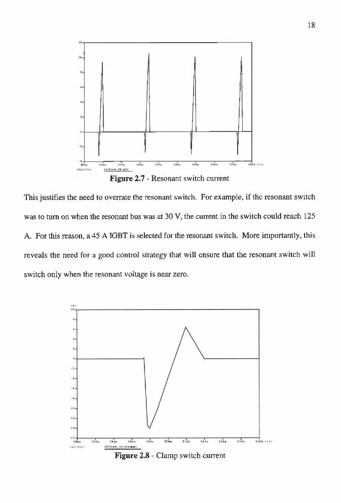
Figure 2.7 - Resonant switch current
This justifies the need to overrate the resonant switch. For example, if the resonant switch
was to turn on when the resonant bus was at 30 V, the current in the switch could reach 125
A. For this reason, a 45 AIGBT is selected for the resonant switch. More importantly, this
reveals the need for a good control strategy that will ensure that the resonant switch will
switch only when the resonant voltage is near zero.
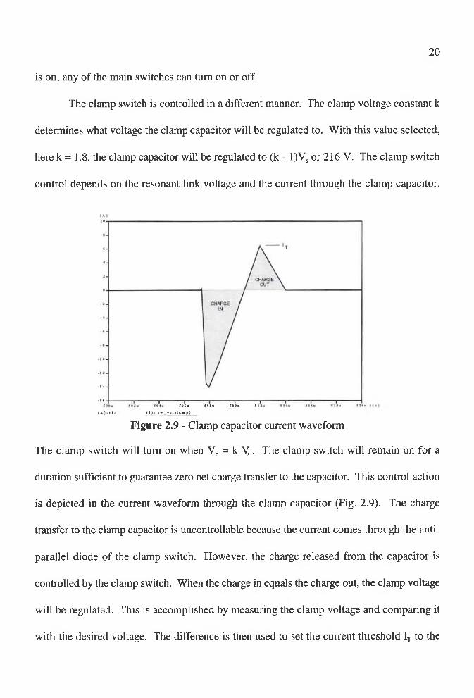
Figure 2.8 - Clamp switch current

19
The selection of the clamp switch is more straight forward than that of the resonant
switch. Because there is a greater impedance in the current path when the clamp switch is
turned on, there is a reduced likelihood that a large current will be drawn. Using the same
simulation as for the resonant switch, the maximum clamp switch current was found to be
14 A. For this switch a device with a 30 A rating would be sufficient, however, for
convenience another 45 AIGBT was selected.
2.4 CONTROL OF RESONANT AND CLAMP SWITCHES
In an ideal circuit, the resonant link would resonate continuously with no added
energy necessary. However, since the inductor and capacitor have some resistance associated
with them, there must be a way to add energy to these resonant components. If energy is not
added to the resonant link, it will eventually lose resonance and become a dc voltage. Such
an event would be damaging to the inverter. The inverter is designed so that it will switch
only when the resonant link is at zero volts. This prohibits the occurrence of a “shoot
through”. A shoot through occurs when both a lower and upper switch in an inverter are
turned on simultaneously, which effectively short circuits the power source. This is another
advantage of an RDCL compared to a PWM inverter.
The resonant switch control depends on two signals, the resonant link voltage and the
inductor current. The control signal will turn on the switch when the link voltage reaches
zero volts. This creates a zero switching loss situation. The device will stay on until the
inductor current reaches a value that equals the current drawn by the load (Id), plus some
minimum value (In,). By increasing the inductor current to In,, the link voltage will increase
to the proper value and resonance will be sustained. During the time that the resonant switch
20
is on, any of the main switches can turn on or off.
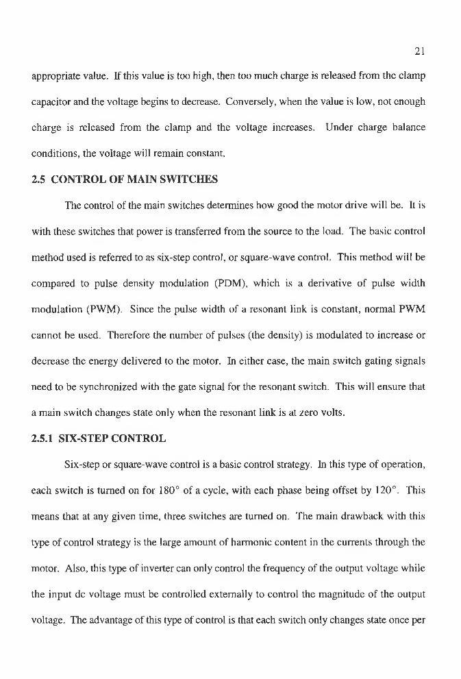
The clamp switch is controlled in a different manner. The clamp voltage constant k
determines what voltage the clamp capacitor will be regulated to. With this value selected,
here k = 1.8, the clamp capacitor will be regulated to (k - 1)VS or 216 V. The clamp switch
control depends on the resonant link voltage and the current through the clamp capacitor.
Figure 2.9 - Clamp capacitor current waveform
The clamp switch will turn on when Vd = k Vs . The clamp switch will remain on for a
duration sufficient to guarantee zero net charge transfer to the capacitor. This control action
is depicted in the current waveform through the clamp capacitor (Fig. 2.9). The charge
transfer to the clamp capacitor is uncontrollable because the current comes through the anti
parallel diode of the clamp switch. However, the charge released from the capacitor is
controlled by the clamp switch. When the charge in equals the charge out, the clamp voltage
will be regulated. This is accomplished by measuring the clamp voltage and comparing it
with the desired voltage. The difference is then used to set the current threshold IT to the
21
appropriate value. If this value is too high, then too much charge is released from the clamp
capacitor and the voltage begins to decrease. Conversely, when the value is low, not enough
charge is released from the clamp and the voltage increases. Under charge balance
conditions, the voltage will remain constant.
2.5 CONTROL OF MAIN SWITCHES
The control of the main switches determines how good the motor drive will be. It is
with these switches that power is transferred from the source to the load. The basic control
method used is referred to as six-step control, or square-wave control. This method will be
compared to pulse density modulation (PDM), which is a derivative of pulse width
modulation (PWM). Since the pulse width of a resonant link is constant, normal PWM
cannot be used. Therefore the number of pulses (the density) is modulated to increase or
decrease the energy delivered to the motor. In either case, the main switch gating signals
need to be synchronized with the gate signal for the resonant switch. This will ensure that
a main switch changes state only when the resonant link is at zero volts.
2.5.1 SIX-STEP CONTROL
Six-step or square-wave control is a basic control strategy. In this type of operation,
each switch is turned on for 180° of a cycle, with each phase being offset by 120°. This
means that at any given time, three switches are turned on. The main drawback with this
type of control strategy is the large amount of harmonic content in the currents through the
motor. Also, this type of inverter can only control the frequency of the output voltage while
the input dc voltage must be controlled externally to control the magnitude of the output
voltage. The advantage of this type of control is that each switch only changes state once per

22
cycle. When output power increases, larger switches require longer times to turn on and off.
If the inverter is used in a hard switched mode (non resonant), there can be large switching
losses and large voltage spikes due to the high current derivative rates. This creates the need
to add snubber circuits across the power devices so voltage limits are not exceeded. By using
a resonant link, switching losses nearly go to zero and the voltage stress across the power
devices is based on the resonant voltage. This gives the designer the ability to go to higher
switching speeds and take advantage of other control strategies.
2.5.2 PULSE DENSITY MODULATION CONTROL
Pulse density modulation is used in this thesis to reduce the harmonic content in the
output of the drive. As mentioned earlier, PDM is the combination of PWM and a resonant
link. Therefore, for the purpose of this discussion, the control will be referred to as PWM.
There is little penalty to using this control method because of the lack of switching losses in
the circuit. The advantage of PWM is that both the voltage and frequency of the output
voltage can be adjusted with this type of control. Sinusoidal-PWM is used in this effort and
will be discussed in detail.
Because the desired inverter output is sinusoidal, a sinusoidal control voltage is
compared with a triangular waveform to generate the necessary gate signals as shown in Fig.
2.10. When the control voltage is greater than the triangle wave, the output is tied to the
positive dc bus. The output is tied to the negative dc bus when the control voltage is less
than the triangle wave. The frequency of the triangle wave establishes the inverter switching
frequency and varies with the control voltage in frequency. The peak voltage of the triangle
wave is a constant. The ratio of the triangle wave frequency, f x, and the control voltage

23
frequency,/), is known as the frequency-modulation ratio zn^and is defined as
f smf = T (2.20)
Ji
Therefore, the maximum inverter switching frequency is For the purposes of this
thesis, mf will be varied to determine the effect on the output harmonics of the inverter. If
mf = 24 (the maximum ratio for this thesis) and the fundamental frequency is 60 Hz, f s would
then be 1440 Hz. This switching frequency is substantially low for the power devices being
used. The output frequency is controlled by changing the frequency of the control voltage
and the switching frequency changes automatically to keep a constant mf.
Figure 2.10 - Sine and triangle waveforms for PWM generation
The output voltage is controlled by varying the magnitude of the control voltage. A
typical PDM waveform is shown in Fig. 2.11. A decrease is magnitude will create a
situation where the triangle wave is greater than the control voltage for a longer period of
time. This lowers the total on-time for the upper power devices which lowers the average

24
Figure 2.11 - Pulse width modulation waveform for mf = 12
voltage per cycle. The control voltage is changed by varying a speed control constant, M.
This constant controls not only the control voltage amplitude, but the frequency of the
control voltage and the switching frequency of the inverter. Using this type of control the
speed can be easily changed by varying one value, while keeping a constant V/f ratio. This
ratio must remain constant to keep the air-gap flux constant so the motor is able to supply
its rated torque and losses are kept within their rated values.

CHAPTER 3
FABRICATION OF RDCL MOTOR DRIVE
The motor drive consists of three separate parts; the source, the resonant dc link and
the inverter. A 270 Vdc source is used to be compatible with advanced aircraft power
systems. The inverter is a standard full bridge design based on IGBTs. The drive is
controlled by a digital controller implemented with a digital signal processor (DSP). The
drive will control an induction motor based blower motor which is used as the load.
Figure 3.1 - Three parts of motor drive
3.1 DIGITAL CONTROL CIRCUITRY
The digital controller, shown schematically in Fig. 3.2, serves three purposes; 1) it
creates the gate signal for the resonant switch, 2) it synchronizes the inverter gate signals
25

26
< < CD m o0) CD CD d ) CD a © S> CD (DCO Q . «£ 5 co ■ CL 2 £(0 O . ro o co Q . 2 o B CL 2 o
JZ 23 x z b _ c 3 . c — x : 3 _c —CL 0l CL CL CL CL
o |o a |o o |o
23 5 3 2o t
A As
A A
Figu
re 3
.2 -
Sche
mat
ic o
f dig
ital c
ontro
ller
TIM
ER
m
coS <
CO <u__ coo co- b - ccQ.oO
coS e n
<S) CD__ coo coC CLOO
coS o
CO CD — </> o coc Q .oo

27
with the resonant gate signal and 3) it amplifies all the gate signals to an appropriate level
for the power devices. The resonant switch gate signal is generated with a 555 timer. The
timer outputs a square wave at a frequency of 42 kHz and a duty cycle of 12%. This signal
is then synchronized with all the inverter gate signals through a D flip-flop to ensure that the
inverter switches change state only when the resonant link voltage is zero. All of the gate
signals are then amplified using driver chips to control the power devices.
The control circuitry consists of two parts. A DSP system generates the necessary
inverter gate controls for all three phases. A TTL based controller generates the resonant
switch gate control and amplifies all the control signals to the appropriate values for the gate
signals for the power devices. The inverter gate signals, for pulse density modulation, are
generated by comparing sine waves with a triangle wave. The sine waves are generated
using a speed control constant, M. These signals are generated as follows,
sin(a) = Af sin(2Mit/11) (3,1)
This generates a control signal that will have a constant V/f ratio for any value of M. The
other two phases are offset ±120° from phase A. The signals are compared with a triangle
wave to generate the appropriate gate controls. This is accomplished by generating a triangle
wave at a frequency f s, a multiple of the fundamental frequency/;. The ratio o f / , t o / ; is
known as the frequency-modulation ratio mf, and will be varied from 12 to 24 for this thesis.
The triangle wave is generated in three parts, based upon a modified time scale multiplied
by mf. Each part is a simple linear equation, all with slopes that are equal in magnitude. The
modified time scale is then reset after each cycle of the triangle waveform for continuous
operation. The sine wave is compared with the triangle wave, and if greater, a logic 1 is

28
Figure 3.3 - Three sections of the triangle waveform
output. Three outputs, one for each phase, are then output through the digital I/O board.
These signals are sent to the controller board through fiber optic cables, where they will be
conditioned to generate the inverter gate signals .
3.2 RESONANT LINK INDUCTOR DESIGN
The resonant inductor plays an important role in the overall efficiency of the RDCL
converter. The resonant inductor accounts for approximately one-third of all losses in this
motor drive, therefore it is important to keep the equivalent series resistance (esr) as low as
possible to minimize the inductor losses. There are two basic equations used to determine
the range for an acceptable number of turns in an inductor. The first one deals with limiting
the volt-second product across the inductor so the core does not enter saturation. This
equation is expressed [9] as
4.44/ABJ 1(3.2)
29
The second limiting equation is derived on the basis of the maximum flux density being
generated by the peak current. Since this inductor uses a cut core, the effective cross
sectional area of the core will be larger due to the fringing flux in the gap. This is
accommodated by adding the gap width to all sides of the core and recalculating the cross
sectional area. Therefore, if the gap is small compared with the size of the core, it can be
assumed that there is no change in the cross sectional area of the core. The maximum
number of turns permitted on a core is found [9] to be
B IN < (3.3)
K, t
for any given core with maximum flux density Bmax.
In this design of a resonant inductor, the pertinent parameters are:
(1) Core constructed of two E cores made of 3C85 ferrite material
(2) Average applied voltage is 190 V
(3) Resonant frequency is 45 kHz
(4) Average current is 17 A
(5) Gap will be 50 mils (0.127 cm)
(6) L = 40pH
From these parameters the apparent power is
S = VA = 3230 VA (3.4)

30
The area product is [9]
A =1 VAxlO4 X1 14
4.44B fK KtnJ u j
= 1.09 cm' (3.5)
A Philips E75 core was selected that has an area product of 1.25 cm4. A range can be
determined for the number of turns permitted using equations 3.2 and 3.3.
N > 4.89 turns (3.6)
N < 29.8 turns (3.7)
Knowing the limitations for the number of turns on the inductor, the appropriate number is
found to obtain the desired inductance. This becomes an iterative process in which core size,
gap size and the number of turns are varied until the number of turns falls within its range.
There are other considerations that must be taken into account as well, for example whether
the number of turns for the necessary wire size can fit into the core's window. All these
factors must be considered when designing an inductor. The number of turns needed is [9]
N =0.4rcA .xl0 8
= 10.9 turns (3.8)
The effect of the fringing flux is found, called the Fringing Flux Factor [9].
F = 1 + A ... 2 0In — = 1.2 (3.9)
We recalculate the number of turns.
lgL 9.98 turns0.4itA FxlO"
(3.10)
Since this number falls within the range found previously, the present design is acceptable
N =
31
up to this point. The next step is to determine the appropriate wire size. This is done by
looking at the current density and then determining the bare wire size AW(B).
J - k. ApQA1 = 793.7 —cm
(3.11)
IA W(B) - — - 0.021 cm 2 = 4225 cmils (3.12)J
From this number, it is determined that three strands of 60/36 gauge litz wire can be used
with a bare wire size of 4500 cmils. Now that the wire size and number of turns are known,
some calculations can be done to estimate the resistance of the winding and determine the
power loss of the inductor. The resistance of the winding is [9]:
R = M L T x N x Rwx q x 10'6 (3.13)
where MLT is the mean length turn, Rw is the linear resistance of the wire at 20°C and is
the resistance correction factor for wire resistance at temperatures between -50° and 100°C.
From this expression the resistance is
R = 29.9 mfl (3.14)
The losses in the copper are now found to be
Pcu = I 2R = 8.65 W (3.15)
The ferrite loss Pfe and the gap loss Pg are then found [9] as shown below
Pf ~ core lossKvolume = 4.5 Wfe
P = K iD l fB „ = 19.03 Wg g J m
(3.16)
(3.17)
where K, is the gap loss coefficient and D is the ferrite width. These three power losses are
combined to find the total power loss for the inductor.
PY = P + Pf + P = 32.18 W22 cu fe g (3.18)

32
Using this design data, an inductor was fabricated in the laboratory and the measured
inductance was 40.8 gH with a resistance of 37 mfl. The resistance was higher in the
experimental inductor because it was wound by hand and therefore was loose in several
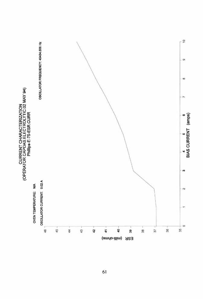
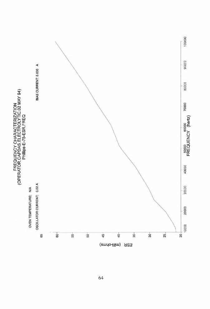
places. The measured data for the resonant inductor can be found in Appendix C.
CHAPTER 4
EXPERIMENTAL RESULTS OF RDCL MOTOR DRIVE
This chapter describes the experimental results of the RDCL motor drive.
Experimental results are shown for six-step and pulse density modulation control, with the
motor under no-load and load conditions. During the experimental portion of the
investigation, the active clamp was not implemented due to its complexitiy and the fact that
it is not needed to accomplish the objective of this thesis. The clamp’s sole purpose is to
limit the peak voltage of the resonant link so lower voltage parts can be used. This was
compensated for by using 1200 V components in the inverter.
4.1 RDCL VOLTAGE AND CURRENT WAVEFORMS
The input to the RDCL is 270 Vdc. A Sorenson DCR300-9B 300 V, 9 A, power
supply was used as the source. The resonant link created an ac disturbance with a peak to
peak amplitude of about 60 volts on the dc source. This would be a problem on larger motor
drives, however, it could be reduced by using a dc filter capacitor on the input. The source
current is the same as the inductor current, and is a sine wave with almost no harmonic
content due to the resonance between the inductor and the capacitor. The fundamental
frequency is 40.5 kHz, with an rms rating of 16 amps. The source voltage and current can
be seen in Fig. 4.1.
33

34
Figure 4.1 - Source voltage and current waveforms
The control of the resonant switch is important to the efficient operation of the
circuit. The resonant period changes from cycle to cycle because the energy stored in the
resonant inductor changes. This creates a situation where the resonant switch will frequently
short the resonant link when there is a voltage present, causing current spikes through the
switch. It was difficult to see the resonant link being shorted by looking at the voltage
waveform in Fig. 4.2. This waveform compared nicely to the simulated waveform of Fig.
2.7. The amplitude and shape were very similar except for the negative pulse in the
simulation. A small resistance was added in this path to reduce the amplitude of these
pulses. The average power lost across this device was estimated to be 30 watts.
Theoretically this loss should be nearly zero. This loss was considerably higher than
expected due to the shorting of the resonant link capacitor. A more sophisticated analog
control circuit is needed to more efficiently perform this function.

35
tune (jia)
Figure 4.2 - Resonant switch current
The resonant DC link voltage and current waveforms are shown in Fig. 4.3. These
waveforms are similar to the simulated waveforms in Fig. 1.4. The obvious difference is the
lack of clamping in the experimental waveforms. It is easy to determine when the resonant
switch was turned on by the increase in the voltage derivative near zero. All inverter
switching is accomplished at this time, so to ensure zero voltage switching, the resonant
switch must be turned on when the resonant bus is at zero volts.
time (pi)Figure 4.3 - Resonant DC link current and voltage waveforms
36
4.2 NO-LOAD MOTOR DRIVE RESULTS
This section describes the results of the motor drive obtained under no-load
conditions. The performance of the RDCL and the different inverter control strategies will
be discussed. The motor drive was tested with four different inverter control strategies:
1. ) Six-step control2. ) Pulse density modulation with modulation frequency ratio = 123. ) Pulse density modulation with modulation frequency ratio = 184. ) Pulse density modulation with modulation frequency ratio = 24
No-load test results indicated that none of these control strategies demonstrate
superior performance with respect to harmonic content in the motor currents. The pulse
density modulation (PDM) strategies did reduce the lower order harmonics when compared
to the six-step control. The current spectra of the six-step and PDM-24 control strategies is
Figure 4.4 - No-load current spectra for a) six-step and b) PDM-24 controls
shown in Fig. 4.4. Note that the PDM-24 has more harmonic “noise” than that of the six-
step, but the peak magnitudes are significantly smaller. This is also evident in the current
waveforms, where the peak current was greater than 3 amps for the six-step control and less
than 2 amps for all the PDM waveforms. Overall, all of the PDM control strategies

37
demonstrated similar behavior. One advantage noticed was that as the modulation frequency,
mf, increases, the motor requires less input power to spin at the same speed. There was a 3%
Percent of full speed
Figure 4.5 - Average source current for various control strategies under no-load
improvement in this area in each step as ^ in c reased from 12, to 18, to 24. In the case of
six-step control, the source current was 10% higher than when PDM was used. The average
source current is shown in Fig. 4.5. In the case of the six-step control, the source voltage was
lowered proportionally to the speed, which accounts for the observed decrease in the source
currents. The data for the PDM control is fairly linear except for the PDM-18 case.
The measured efficiencies of the drive for the various control strategies are shown
in Fig. 4.6. The results indicate that as the modulation frequency goes up, the efficiency
decreases. The efficiency decreases at lower speeds because the output power decreases, and
the input power remains nearly the same. This occurs because a constant amount of energy
is needed to ensure the voltage bus continues to resonate. This is a disadvantage of the
RDCL topology. At low output power, the motor drive becomes inefficient due to the
“overhead” power needed to keep the voltage bus in resonance. Overall, the efficiencies are
38
Motor speed (rpm)
Figure 4.6 - Efficiencies for various control strategies under no-load
considerably lower than expected. The theoretical losses were found to be 30 watts using
equation 2.15. This results in an efficiency of 95%. The six-step control strategy efficiency
improves at lower speeds because the source voltage is lowered to maintain a constant V/f
ratio. This creates a smaller resonant link current and therefore lower losses. A dc/dc
converter would have to be inserted between the source voltage and RDCL inverter to make
a proper comparison between the six-step and PDM control strategies.
The motor drive was tested over a 5:1 speed range. This section discusses the
performance of the motor drive in terms of its ability to control the speed of the machine and
maintain a constant V/f ratio. The no-load full speed of the machine was measured to be
3600 rpm, which is also the synchronous speed of the machine. Under no-load conditions,
the slip should be nearly zero, which it is in this case. The speed of the machine can be
predicted by multiplying the speed factor cspeed (ratio to full speed) times 3600 rpm because
the slip is near zero. All of the control strategies generated accurate speed results. The
results also showed that the voltage to frequency ratio was kept constant (Fig. 4.7). The

39
Percent o f full speed
Figure 4.7 - V/f ratio for various control strategies under no-load
PDM control did not create a high mean voltage however, only around 160 V, compared to
200 V for the six-step control. This is because there is more dead time with PDM control
compared with six-step control, therefore, the theoretical maximum output voltage is lower
with PDM control.
4.3 FULL-LOAD RDCL MOTOR DRIVE RESULTS
The various control strategies had a more significant impact on the performance of
the motor drive under full-load. The results show that PDM control has advantages over six-
step control. Also, as the modulation frequency is increased improved performance is
realized. The current spectra for the output current are shown in Fig. 4.8. The results show
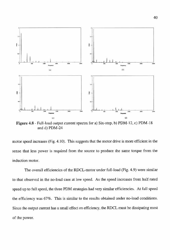
that PDM reduces the lower order harmonic components in the range to 500 Hz and
improves the total harmonic distortion (THD). The THD at full speed for six-step control
is 38%, while for PDM-24 it is 13%. As my is increased, the lowest harmonic is shifted to
higher frequencies and the magnitude of the higher harmonic frequencies also decreases.
The measured average source current decreases as mf increases. It was also observed that the
40
(c) (d)Figure 4.8 - Full-load output current spectra for a) Six-step, b) PDM-12, c) PDM-18
and d) PDM-24
motor speed increases (Fig. 4.10). This suggests that the motor drive is more efficient in the
sense that less power is required from the source to produce the same torque from the
induction motor.
The overall efficiencies of the RDCL-motor under full-load (Fig. 4.9) were similar
to that observed in the no-load case at low speed. As the speed increases from half rated
speed up to full speed, the three PDM strategies had very similar efficiencies. At full speed
the efficiency was 67%. This is similar to the results obtained under no-load conditions.
Since the output current has a small effect on efficiency, the RDCL must be dissipating most
of the power.

41
Motor speed (rpm)
Figure 4.9 - Efficiencies for various control strategies under full-load
Similar to the no-load case, the performance of the motor drive is evaluated in terms
of its ability to control the speed of the machine. The expected speed of the machine can be
estimated by noting that the synchronous speed is 3600 rpm and the rated speed is 3400 rpm.
This gives the slip to be 5.6% and the slip frequency (fsl) is found to be 3.3 Hz. The equation
[8] T = k (speed.)2 is used to calculate the speed of the machine at any other point. For
120example at half speed, f sl = 0.83 Hz. The slip speed (nsl), is nsl = ------- x / z = 50 rpm .poles
The expected speed is found to be n = ns - nsl = 1750 rpm. This is proven to be accurate
based on the experimental data. In the case of the six-step control, the half speed was
experimentally found to be 1740 rpm. The speed of the machine for the various control
strategies is seen in Fig. 4.10. Recall that when PDM control was used, the output voltage
was lower than necessary. Consequently, the full-load speed of the machine when PDM
control was used was lower than it should have been. This could be corrected by increasing
the source voltage to the appropriate level.
42
Percent of full speed
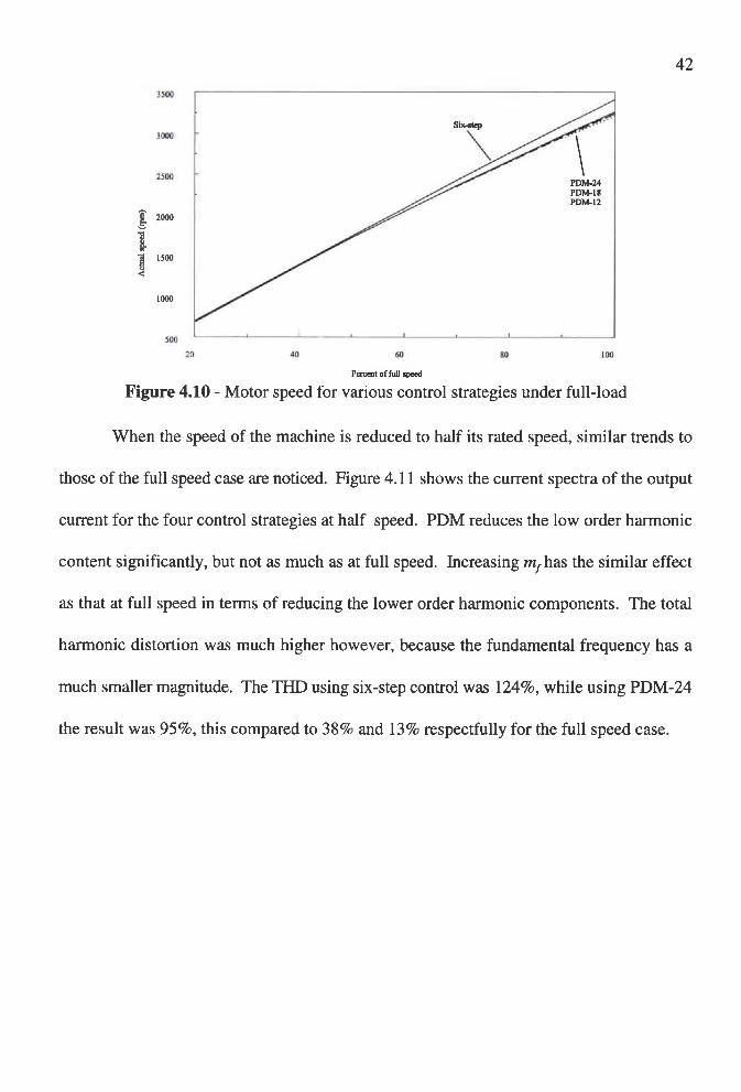
Figure 4.10 - Motor speed for various control strategies under full-load
When the speed of the machine is reduced to half its rated speed, similar trends to
those of the full speed case are noticed. Figure 4.11 shows the current spectra of the output
current for the four control strategies at half speed. PDM reduces the low order harmonic
content significantly, but not as much as at full speed. Increasing mf has the similar effect
as that at full speed in terms of reducing the lower order harmonic components. The total
harmonic distortion was much higher however, because the fundamental frequency has a
much smaller magnitude. The THD using six-step control was 124%, while using PDM-24
the result was 95%, this compared to 38% and 13% respectfully for the full speed case.

43
Figure 4.11 - Full-load spectra for a) six-step, b) PDM-12, c) PDM-18 and PDM-24 operating at half speed
CHAPTER 5
CONCLUSIONS
An actively clamped resonant dc link inverter was designed and simulated to control
an induction motor - blower in an adjustable speed application. The objective of this thesis
was to build and test an RDCL inverter and compare the performance of a six-step control
strategy with a PDM strategy using constant V/f open-loop speed control. The use of PDM
showed advantages over six-step control by reducing the lower order harmonic content in the
output current of the motor drive. This improvement was also observed as the PDM
modulation ratio increased. The performance gains were more evident under full-load, but
were also seen at no-load. As motor speed increased, the performance of the drive improved
in both efficiency and total harmonic distortion.
The control of the RDCL presents a significant challenge. One of the keys to
efficient operation of the RDCL is the proper control of the resonant link switch. Although
performance gains were evident with the simple control method used for the resonant switch,
more substantial improvements would occur if an adaptive controller were employed to
ensure the resonant switch is tumed-on only when the resonant voltage bus is zero. This
control deficiency of the resonant switch resulted in significant losses in the RDCL circuit.
This impacted the overall efficiencies of the motor drive which were lower than expected.
44

45
This shows that the majority of the losses were in the RDCL and that a small percentage was
due to conduction losses. It was also found that as mf increased, the efficiency lowered. This
also shows that switching losses were more prominent than expected.
Another challenge is to produce resonant components with high quality factors. If
these components have high equivalent series resistances then more energy must be delivered
to them so the link voltage will resonate and return to zero. As more energy is delivered to
the resonant components, the peak voltage increases to more than the minimum 2VS. When
this technology is applied to advanced aircraft power systems, with a nominal source voltage
of 270 vdc, the peak voltage could exceed 600 V. This creates a situation where 1200 V
power switches must be used.
Various techniques can be used to limit the peak voltage, including passive and active
clamping. Active clamping can limit the peak voltage to as low as 1.3VS, while passive
clamping can limit to 2VS. Placing an active clamp across the resonant circuit presents
significant difficulties. Essentially, active clamping attempts to maintain a net energy
balance in the clamp capacitor, thereby regulating the clamp capacitor voltage.
The open-loop variable speed control is accomplished by maintaining the air gap flux
constant which is done by ensuring that the voltage/frequency ratio constant. It has been
shown that the control circuitry accomplished this task. In the case of PDM control the
average output voltage was low which caused the motor to spin at a slower speed under load.
This could be corrected by increasing the source voltage to account for this shortfall.
This investigation has shown that the use of PDM with a resonant link has
benefits compared to a standard six-step control. These benefits include improved total

46
harmonic distortion and efficiency. The PDM modulation ratio can be increased to improve
this advantage without significant penalty. An induction motor was effectively controlled
by keeping the voltage/frequency ratio constant. The performance benefits may also be
realized in applications with more rigorous motor control performance specifications. RDCL
inverters coupled with flux vector or variable structure motor control strategies may have
some performance advantages over current power electronics/motor control topologies.

REFERENCES
[1] D.M. Divan, "The Resonant DC Link Converter-A New concept in Static Power Conversion," Conf. Rec. IEEE IAS Annual Meeting, 1986, pp. 648-656.
[2] D.M. Divan and G. Skibinski, "Zero Switching Loss Inverters for High Power Applications," Conf. Rec. IEEE IAS Annual Meeting, 1987, pp. 627-634.
[3] J.S. Lai and B.K. Bose, "An Improved Resonant DC Link Inverter for Induction Motor Drives," Conf. Rec. IEEE IAS Annual Meeting, 1988, pp. 742-748.
[4] T.M. Jahns, R.W. De Doncker, A.V. Radun, P.M. Szczesny, and F.G. Turnbull, "System Design Considerations for a High-Power Aerospace Resonant Link Converter," Applied Power Electronics Conf, 1992, pp. 665-673
[5] Analogy®, Inc, “Saber Reference Manual, Release 3.1a,” 1987.
[6] Phillips Components, “Ferrite Materials and Components Catalog.”
[7] M.H. Rashid, “Power Electronics: Circuits, Devices, and Applications,” Prentice- Hall: Englewood Cliffs, NJ, 1988.
[8] N. Mohan, T.M. Undeland, W.P. Robbins, “Power Electronics: Converters, Applications, and Design,” John Wiley and Sons, New York, NY, 1989.
[9] W.T. McLyman, “Transformer and Inductor Design Handbook,” Dekker, New York, NY, 1988.
47

APPENDIX A
DIGITAL SIGNAL PROCESSOR PROGRAMS
48

PWM2.C
in c lu d e "ilic30.h"#include" c :\dsp2\ti\include\math.h"
void main(void);float OurMaxf float numl, float num2 ); void Ini tDSP( void);
void SendCommand(CommandType command);
float OurMaxf float numl, float num2);
/************************************************************************/
typedef struct {MixedType * buf_start; MixedType * buf_end;
} Buffer;
MixedType *pc_data, *pc_data_end;
int k=l;
unsigned long dummy;
bool running = FALSE, logging = TRUE; float timeLimit = -1;
float loghits=0.0,adchits=0.0,controlhits=0.0,DMAhits=0,0;
float OurMaxf float numl, float num2 ){if (numl>num2)
return numl;else return num2;}
void InitDSP(void){
/ * * * * * * * * * * * * * * * * * TNTTT AT .I7.F. C30 DSP BOARD **********************/ *PRIMCTL = PRIMWD;*EXPCTL = EXPWD;
/*********** INITIALIZE 32 CHANNEL DIGITAL I/O BOARD *************/ dummy = *DIG32_RESET;*DIG32 CONTROL = DIG32_CONTROL_CONFIG;
49

PWM2.C
*DIG32_PORT_CONFIG = DIG32_ALL_PORTS_SINGLE_BUFFERED;
y***************** j f i jm AT .T7F. TIMERS *****************************/ *TIMER_CONTROL_0 = 0x200; /* CLKSRC = 1/2 H l (internal) */*TIMER_PERIOD_0 = 0xee2elefc;*TTMER_CONTROL_01= OxOcO; /* reset & start timer */
}
float time=0.00;float inADC[32], encO, oldtime, newtime;int count = 0;unsigned int digitalOut=0;unsigned long digital_out;
float sin_a, sin_b, sin_c;float M = 1.0;float sample, tmod, tri;/************************4t***********#*#***********************’f'**#**4t**4y /***£********************************************************************y
void main(){
long command;int i, index;int tempCount;
InitDSP();
*((ulong *) DSP_COMMAND) = 0;
pc_data = (MixedType *) DATA;
(pc_data)->fp=1.0; /* initialize M to 1.0 */
/* let the PC know we’re up and running */
*((ulong *) PC_PARAMS) = XFER_ITEM_SIZE;
index =0;
while(l){M = (pc_data)->fp;
time = *TIMER_COUNTER_0 / 8.325e6;
sin_a = M*sin(M*2.0*PI*60.0*time);
50

PWM2.C
sin_b = M*sin(M*2.0*PI*60.0*time - 2.0*PI/3.0);sin_c = M*sin(M*2.0*PI*60.0*time + 2.0*PI/3.0);
sample = time*12.0*M*60.0;tmod = (sample - (ceil(sample) -1 .0)) / (12.0*M*60.0);
if ( (O.Octmod) & & ( tmod<=(1.0/(48.0*M*60.0))) ){tri = -48.0*M*60.0*tmod;}
else if ( ((1.0/(48.0*M*60.0))<tmod) && (tmod<=(1.0/(16.0*M*60.0)))){tri = 48.0*M*60.0*tmod - 2.0;}
else if ( ((1.0/(16.0*M*60.0))<tmod) && (tmod<=(1.0/(12.0*M*60.0)))) {tri = -48.0*M*60.0*tmod + 4.0;}
if (sin_a > tri)digital_out = 0x00010000;
else digital_out = 0x00000000;
if (sin_b > tri)digital_out = digital_out 10x00020000;
if (sin_c > tri)digital_out = digital_out 10x00040000;
*DIG32_PORT_A = digital_out;}
51

6STEP.C
#include "ilic30.h"#include "c:\dsp2\ti\include\math.h"
void main(void);float OurMax( float num l, float num 2);void InitDSP(void);
void SendConunand(CommandType command);
float OurMax( float num l, float num2);
/************************************************************************/
typedef struct {MixedType * buf_start; MixedType * buf_end;
} Buffer;
MixedType *pc_data, *pc_data_end;
int k= l;
unsigned long dummy;
bool running = FALSE, logging = TRUE; float timeLimit = -1;
float loghits=0.0,adchits=0.0,controlhits=0.0,DMAhits=0.0;
float OurMax( float num l, float num2 ){if (numl>num2)
return num l;else return num2;}
void InitDSP(void){
y***************** INITIALIZE C30 DSP BOARD **********************/ ♦PRIMCTL = PRIMWD;♦EXPCTL = EXPWD;
/****♦**♦**♦ INITIALIZE 32 CHANNEL DIGITAL I/O BOARD *************/ dummy = *DIG32_RESET;*DIG32_CONTROL = DIG32_CONTROL_CONFIG;
52

6STEP.C
*DIG32_PORT_CONFIG = DIG32_ALL_PORTS_SINGLE_BUFFERED;
/***************** initialize TIMERS *****************************/ *TIMER_CONTROL_0 = 0x200; /* CLKSRC = 1/2 Hl (internal) */*TIMER_PERIOD_0 = 0xee2elefc;*TIMER_CONTROL_0 1= OxOcO; /* reset & start timer */
float time=0.00;float inADC[32], encO, oldtime, newtime;int count = 0;unsigned int digitalOut=0; unsigned long digital_out;
float sin_a, sin_b, sin_c;float M - 1.0;
void main(){
long command;int i, index;int tempCount;
InitDSP();
*((ulong *) DSP_COMMAND) = 0;
pc_data = (MixedType *) DATA;
(pc_data)->fp=1.0; /* initialize M to 1.0 */
/* let the PC know we're up and running */
*((ulong *) PC_PARAMS) = XFER_ITEM_SIZE;
index =0;
while(l){M = (pc_data)->fp;
time = *TIMER_COUNTER_0 / 8.325e6;
sin_a = sin(M*2.0*PI*60.0*time);sin_b = sin(M*2.0*PI*60.0*time - 2.0*PI/3.0);
53

6STEP.C
sin_c = sin(M*2.0*PI*60.0*time + 2.0*PI/3.0);
if (sin_a > 0.0)digital_out = 0x00010000;
else digital_out = 0x00000000;
if (sin_b > 0.0)digital_out = digital_out I 0x00020000;
if (sin_c > 0.0)digital_out = digital_out I 0x00040000;
*DIG32_PORT_A = digital_out;}
54

APPENDIX B
NODE EQUATIONS FOR SABER SIMULATION
55

# A CTIV ELY C LA M PED R E SO N A N T D C LIN K - Equivalent C ircuit - acrdcl_eq.sinI -------------------------------------------------- ------------ ---- ----------------------------------------------------# R E SO N A N T CIRC U IT# - ---------- ------------------------- ---------------- ---------v.vin in 0 =270l.lr in vd =40.8u, r=50m , ic=4c.cr vd 0 =333n, esr= l lm , ic=0d .d l 0 vdsw _vc.res vd 0 vd 0 = m odel= (vt= l,vh= .5 ,ron=10m eg,roff= .l)
# C L A M P C IR C U IT
sw _vc. clam p vcl vd vd 0 = model=(vt=486, vh=1.25, ro n = .l, roff=10m eg), icc.cc in vcl =10u, esr=50m , ic=-216#-----------------------------------
LO A D=tfc
i.load vd 0 = dc=7.5
56

# R ESO N A N T CIRC U IT# . . . . ..
v.vin in 0 =270l.lr in vd =40.8u,r=50m , ic=7c.cr vd 0 = 3 3 3 n ,e s r= llm , ic=0d .d l 0 vdsw_14.ql vd 0 gate = roff=10m eg, ron=.01, tr=300n, tf= luclock_14.gate gate = freq=39.6k, duty=.2a __ ______________ _________________
# IN V ER TER C IR C U IT
sw_14.q 11 vd va gate_ap = roff=10m eg, ron=.2, tr=300n, tf=3usw _14.ql2 VC 0 gate_cm = roff=10m eg, ron=.2, tr=300n, tf=3usw _14.ql3 vd vb gate_bp = roff=10m eg, ron=.2, tr=300n, tf=3usw _14.ql4 va 0 gate_am = roff=10m eg, ron=.2, tr=300n, tf=3usw _14.ql5 vd vc gate_cp = roff=10m eg, ron=.2, tr=300n, tf=3usw _14.q!6 vb 0 gate_bm = roff=10m eg, ron=.2, tr=300n, tf=3uclock_14.gate_ap gate_ap = freq=60, duty==.5clock_14.gate_.am gate_am ■= freq=60, duty=.5, td = l/ l 20clock_14.gate_bp gate^bp = freq=60, duty==.5, td= l/180clock_14.gate_bm gate_bm = freq=60, duty=.5, v l= _ l , v2=_0, t d = l / l80clock_14.gate_cp gate_cp = freq=60, duty==.5, v l= _ l , v2=_0, td= l/360clock_14.gate_.cm gate_cm ■■= freq=60, duty=.5, td= l/3 6 0d .d l l va vdd .d l2 0 vcd .d l3 vb vdd .d l4 0 vad .d l5 vc vdd .d l6i t . _ ___
0 vb
# M O TO R LO A D
r.a va val = lur.b vb vbl = lur.c vc v c l = lur.rea v a l va2 =4Ilea va2 va3 =29mr.r2a va3 ntrl =8r.rea v a l ntrl =550l.lma v a l ntrl = 522mr.reb v b l vb2 =4l.leb vb2 vb3 =29mr.r2b vb3 ntrl =8r.reb v b l ntrl =550l.lm b vbl ntrl =522mr.rec v c l vc2 =4l.lec vc2 vc3 =29mr.r2c vc3 ntrl =8r.rcc v c l ntrl =550l.lmc v c l ntrl =522mr.rn ntrl 0 =100g
57

#------------------------------------------------------------------------------------------------------- ---------------------------# A C TIV ELY C LA M PED R E SO N A N T D C LIN K IN V ER TER - acrdcl_6step.sin# ------------------------------------------------------------------------------------------------------ -------------------------------------# R E SO N A N T C IR C U IT# ----------------------------------------------------------------v.vin in 0 =270l.lr in vd = 40 .8u, r=50m , ic=4c.cr vd 0 =333n, esr= l lm . ic=0d .d l 0 vdsw_14.q 1 vd 0 gate = roff=10m eg, ron=. 1, tr=300n, tf= 1 uclock_14.gate gate = freq=35k, duty=. 15#---------------------------------— --------------------------# C L A M P C IR C U IT# ------------------------------------------------------------sw_14.clamp vcl vd clm p = roff=10m eg, ro n = .l, tr=3OOn, tf= luclock_14.clmp clm p = freq=35k, duty=.25, td= 11 uc.cc in vcl =10u, esr=50m , ic=-216# ----------------------------------------------------------------# IN V ER TER C IR C U IT#-------------------sw_14.ql 1 vd va gate_ap = roff=10m eg, ron=.2, tr=300n, tf=3usw _14.ql2 VC 0 gate_cm = roff=10m eg, ron=.2, tr=300n, tf=3usw _14.ql3 vd vb gate_bp = roff=10m eg, ron=.2, tr=300n, tf=3usw _14.ql4 va 0 gate_am = roff=10m eg, ron=.2, tr=300n, tf=3usw _l4 .q l5 vd VC gate_cp = roff=10m eg, ron=.2, tr=300n, tf=3usw _14.ql6 vb 0 gate_bm = roff=10m eg, ron=.2, tr=300n, tf=3uclock_14.gate_ap gate_ap = freq=60, duty=.5clock_14.gate_am gate_am = freq=60, duty=.5, td= 1/120c lo ck J4 .g a te_ b p gate_bp = freq=60, duty=.5, td = l / l 80clock_14.gate_bm gate_bm = freq=60, duty=.5, v l= _ l , v2=_0, td= 1/180 clock_14.gate_cp gate_cp = freq=60, duty=.5, v l= _ l , v2=_0, td= l/360 clock_14.gate_cm gate_cm = freq=60, duty=.5, td= 1/360d .d l l va vdd .d l 2 0 VCd .d l3 vb vdd .d l4 0 vad .d l5 VC vdd .d !6 0 vb# ----------------------------------------------------------------# M O TO R L O A D#----------------------------------------------------------------r.a va val = lur.b vb vbl = lur.c vc vcl = lur.rea v a l va2 =4l.lea va2 va3 =29mr.r2a va3 ntrl =200kr.rea v a l ntrl =550Lima v al ntrl =522m, ic= -l .25r.reb vbl vb2 =4l.leb vb2 vb3 =29mr.r2b vb3 ntrl =200kr.reb v b l ntrl =550Limb v b l ntrl =522m , ic=0r.rec v c l vc2 =4l.lec vc2 vc3 =29mr.r2c vc3 ntrl =200kr.rcc v c l ntrl =550l.lmc v c l ntrl =522m, ic=1.25r.m ntrl 0 = 100g
58

APPENDIX C
RESONANT INDUCTOR CHARACTERIZATION CURVES
59

CU
RR
EN
T C
HA
RA
CTE
RIZ
ATI
ON
(O
PE
RA
TOR
.CA
PD
AS
.ELE
CTR
OLY
TIC
.02
MA
Y 94
) P
hilli
ps-E
-75-
IND
.CU
RR
o
BIA
S C
UR
RE
NT
(am
ps)
(sAjuaq-ojoiw) 30NVJL0nC]NI
60
CU
RR
ENT
CH
AR
AC
TER
IZA
TIO
N
(OPE
RA
TOR
.CA
PDA
S.EL
ECTR
OLY
TIC
.02
MAY
94)
Ph
illip
s-E-
75-E
SR.C
URR
BIAS
CU
RR
ENT
(am
ps)
61

a
<
"T"OC'Jco
ao io vd A in v n o
BIAS
CU
RR
ENT
(am
ps)
62

§ooo
(sAiueq-aioiw) aONVlOAONI
FREQ
UEN
CY
(Hz)
63
FREQ
UEN
CY
CH
AR
AC
TER
IZA
TIO
N
(OPE
RA
TOR
.CA
PDA
S.EL
ECTR
OLY
TIC
.02
MAY
94)
Ph
illip
s-E-
75-E
SR.F
REQ
1000
0 20
000
3000
0 40
000
5000
0 60
000
7000
0 80
000
9000
0 10
0000
FREQ
UEN
CY
(her
tz)
64

<
o5
aoiovd Ainvno
FREQ
UEN
CY
(her
tz)
65


