
Turk J Elec Eng & Comp Sci
(2016) 24: 2267 – 2273
c⃝ TUBITAK
doi:10.3906/elk-1312-258
Turkish Journal of Electrical Engineering & Computer Sciences
http :// journa l s . tub i tak .gov . t r/e lektr ik/
Research Article
An implantable microstrip antenna design for MICS-band biomedical applications
Adnan SONDAS∗, Mustafa Hikmet Bilgehan UCAR
Department of Information Systems Engineering, Faculty of Technology, Kocaeli University, Izmit, Kocaeli, Turkey
Received: 30.12.2013 • Accepted/Published Online: 08.07.2014 • Final Version: 15.04.2016
Abstract: In this paper, an implantable microstrip antenna design is introduced to cover the Medical Implant Com-
munications Service (MICS, 402−405 MHz) band for biomedical telemetry systems. The radiating layer of the antenna
comprises two concentric square split-ring elements and a metallic pad placed between them. A shorting pin is also used
for miniaturization purposes, directly connecting the outer ring element to the ground plane. It is numerically demon-
strated that the proposed antenna offers approximately 7% impedance bandwidth and gains of 1.9 dBi at the designated
frequency band. In addition, effects of some critical design parameters on the antenna performance are numerically
examined in the paper, noting that the full-wave analysis of the implant antenna is carried out using CST Microwave
Studio.
Key words: Biomedical telemetry, MICS band, implantable antenna, split-ring elements
1. Introduction
In recent years, considerable progress has been made to develop implantable sensors that can continually monitor
the physiological therapies of patients. The implanted sensors must be able to communicate with external
devices, thus requiring integrated compact antennas. Designing antennas that would operate in a tissue is an
extremely demanding task. Factors such as tissue conductivity, impedance matching, antenna size, low power
requirements, and biocompatibility play significant roles in the design [1–8]. For a realistic antenna simulation,
the dielectric properties and geometry of the tissue should be taken into consideration. Microstrip patch designs
are currently receiving considerable attention for implantable antennas because they are highly flexible in shape
and conformability. Meander-shaped dipole elements [1–3], split-ring elements [4], and different types of slot
elements [5,6] are used in such designs. A detailed review of the implant antenna designs can be found in [7,8].
Implantable antennas are designed to operate at specific frequency bands, namely the Medical Implant
Communications Service (MICS, 402–405 MHz) and/or the Industrial Scientific and Medical (ISM, 2.4–2.48
GHz) [9,10] bands. In this study, we introduce a novel split-ring resonator (SRR)-shaped microstrip antenna
design for biomedical telemetry applications in the MICS band. Due to their compact size and inherent prop-
erties, SRRs have been preferred in microstrip antenna and filter applications [11–14]. Considering implantable
antenna designs in the literature [1–8], the proposed low-loss and low-cost antenna has a compact size of 14 ×14 × 2.54 mm3 (∼0.02 λ0× 0.02 λ0) at 403 MHz, and thus the proposed design can be a good candidate for
MICS-band biomedical applications.
The full-wave analysis of the proposed design has been carried out using CST Microwave Studio, utilizing
∗Correspondence: [email protected]
2267

SONDAS and UCAR/Turk J Elec Eng & Comp Sci
the time-domain finite-integration technique. In this paper, the simulated antenna performance (S11 , radiation
pattern, electric field distribution, and SAR) is presented. Note that this paper is an extended version of [15],
which was previously presented at the ICECCO’2013 conference.
2. Numerical design of the implant antenna
The proposed antenna configuration is depicted in Figure 1. As seen, the radiating layer of the antenna is
composed of a pair of concentric square split-ring elements. A metallic pad with a size of 1 × 1 mm is placed
between the rings near the outer gap. The separation between the outer and inner ring elements is 1 mm
and a coaxial feed is used for excitation. All the metallic elements are sandwiched with substrate/superstrate
structure (Rogers RO3210) with a total thickness of 2h = 2.55 mm, and εr = 10.2 (tanδ = 0.003). A shorting
pin directly connects the outer ring element to the ground plane (GP), allowing for miniaturization. In practical
implementations, the implantable antenna must be operated in a skin, and thus we modeled the antennas at a
depth of 3 mm of a skin (εr = 31.29).
The input reflection coefficient (S11) characteristic of the implant antenna is displayed in Figure 2. As can
be seen, the proposed antenna provides an approximately 7% impedance bandwidth (389−416 MHz) covering
the designated MICS band. Note that the |S11| ≤ −10 dB criterion with 50 Ω system impedance is considered.
Superstrate
Substrateεr
Skin
2h
d
L0
L0
Feeding
Shorting
Pin
L1
L2
W1
g
S
F
GP Pin Coax-feed300 320 340 360 380 400 420 440 460 480 500
-25
-20
-15
-10
-5
0
Frequency (MHz)
S11( dB)
7%
389 MHz 416 MHz
Figure 1. The proposed implantable antenna design: L0
= 14, L1 = 12, W1 = 1.7, g = 1, S = 2.8, F = 11.2, h
= 1.27, d = 3 (all in mm), εr = 10.2.
Figure 2. The simulated return loss characteristics of the
implantable antenna design.
In designing, the size of the loops, the placement of the metallic pad, and the position of the shorting pin
were determined to be critical parameters for achieving the preferred antenna performance in the frequency
band of interest. The design steps depicted in Figure 3 have been employed to reach the optimum S11
2268
SONDAS and UCAR/Turk J Elec Eng & Comp Sci
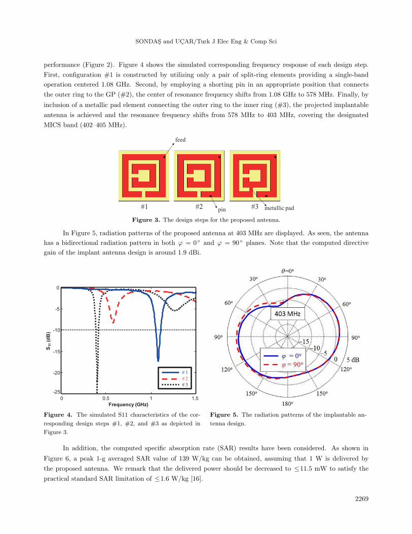
performance (Figure 2). Figure 4 shows the simulated corresponding frequency response of each design step.
First, configuration #1 is constructed by utilizing only a pair of split-ring elements providing a single-band
operation centered 1.08 GHz. Second, by employing a shorting pin in an appropriate position that connects
the outer ring to the GP (#2), the center of resonance frequency shifts from 1.08 GHz to 578 MHz. Finally, by
inclusion of a metallic pad element connecting the outer ring to the inner ring (#3), the projected implantable
antenna is achieved and the resonance frequency shifts from 578 MHz to 403 MHz, covering the designated
MICS band (402–405 MHz).
#1 #2 #3
feed
pin metallic pad
Figure 3. The design steps for the proposed antenna.
In Figure 5, radiation patterns of the proposed antenna at 403 MHz are displayed. As seen, the antenna
has a bidirectional radiation pattern in both φ = 0 and φ = 90 planes. Note that the computed directive
gain of the implant antenna design is around 1.9 dBi.
0 0.5 1 1.5
-25
-20
-15
-10
-5
0
# 1
# 2
# 3
Frequency (GHz)
S11(dB)
Figure 4. The simulated S11 characteristics of the cor-
responding design steps #1, #2, and #3 as depicted in
Figure 3.
Figure 5. The radiation patterns of the implantable an-
tenna design.
In addition, the computed specific absorption rate (SAR) results have been considered. As shown in
Figure 6, a peak 1-g averaged SAR value of 139 W/kg can be obtained, assuming that 1 W is delivered by
the proposed antenna. We remark that the delivered power should be decreased to ≤11.5 mW to satisfy the
practical standard SAR limitation of ≤1.6 W/kg [16].
2269

SONDAS and UCAR/Turk J Elec Eng & Comp Sci
Moreover, the electric field distribution of the proposed implanted antenna at 403 MHz is depicted in
Figure 7, where it is observed that the field distribution is mainly concentrated along the ring elements and the
metallic pad connecting them, proving the critical role of those elements in the proposed antenna’s performance.
Figure 6. The computed specific absorption rate (SAR)
of the implantable antenna design embedded in a simu-
lated part of skin tissue at 403 MHz.
Figure 7. The electric field distribution at 403 MHz.
3. Parametric studies
In order to evaluate the performance of the implantable antenna, a series of parametric studies have been carried
out to display the effects of the critical antenna parameters, namely the feed location, the shorting pin location,
the metallic pad location, and the inner gap location. Below, we briefly discuss these studies.
3.1. Feed location
The proposed antenna is excited by a standard coaxial probe feed and the location of the feed is expected to
change mainly the antenna impedance matching. As can be seen from Figure 8, S11 levels change by changing
the feed location without any shift in the resonance frequency.
3.2. Shorting pin location
A shorting pin can act as a GP and can reduce the electrical size of the antenna [1] for a given frequency. Hence,
by including a shorting pin in the proposed design, the resonance frequency is observed to shift from 738 MHz
to 403 MHz (see Figure 9). It is also observed that the pin location not only affects resonance frequency but
also affects the antenna matching.
3.3. Metallic pad location
The concentric split-ring elements are connected by a 1 × 1 mm metallic pad and the location of the pad
changes the performance of the antenna. To demonstrate the effects of the pad location, we carried out a series
of simulations based on the different pad locations depicted in Figure 10. As can be seen from Figure 11, the
pad location affects both the impedance matching and the resonance frequency of the proposed antenna over
2270

SONDAS and UCAR/Turk J Elec Eng & Comp Sci
the band of 400–580 MHz. For the optimum S11 level and maximum miniaturization effect, the #0 location
for the metallic pad is selected in the ultimate antenna configuration.
300 320 340 360 380 400 420 440 460 480 500–25
–20
–15
–10
–5
0
Frequency (MHz)
S11
(dB
)
0 (Opt.) 2.65.27.810.4
Shi" in - y direction
–2.5 mm 0 (Opt.)2.5 mm
Shi" in x direction
300 350 400 450 500–30
–20
–10
0
Frequency (MHz)
S 11
(dB
)Figure 8. The effects of feed point location on the S11
performance.
Figure 9. The effects of shorting pin location on the S11
performance.
0
1
2
3
4
5
# 0 (Opt .) # 1# 2# 3# 4# 5
Pad Locations
300 400 500 600–25
–20
–15
–10
–5
0
700Frequency (MHz)
S11
( dB
)
Figure 10. Different metallic pad locations. Figure 11. S11 performance of the proposed antenna
design with respect to different pad locations depicted in
Figure 10.
3.4. Inner gap location
The inner square ring element has a size of a 1.7 × 1 mm gap, and the location of this gap may affect the
frequency response of the antenna. The S11 performances of the proposed antenna design with respect to the
different inner gap locations (Figure 12) are depicted in Figure 13. As seen, the inner gap location slightly affects
the resonance frequency (max. 10 MHz). Because of the maximum miniaturization effect, the #0 location is
2271

SONDAS and UCAR/Turk J Elec Eng & Comp Sci
selected in the final antenna configuration. It has also been determined that the inner gap size has a slight
effect on the resonance frequency. The optimum design is achieved where the gap size is 1 mm.
0
1
2
3
300 320 340 360 380 400 420 440 460 480 500–25
–20
–15
–10
–5
0
Frequency (MHz)S
11( d
B)
# 0 (Opt.) # 1# 2# 3
Inner Gap Location
Figure 12. Different inner gap locations. Figure 13. S11 performance of the proposed antenna de-
sign with respect to different inner gap locations as shown
in Figure 12.
4. Conclusions
In this paper, we have introduced a novel implantable antenna design for biomedical telemetry applications in
the MICS (402–405 MHz) band. The proposed compact antenna design (∼0.02 λ0 × 0.02 λ0 @ 403 MHz)
has a pair of concentric square split-ring elements, a metallic pad, and a shorting pin configuration and is
excited by a standard coaxial feed structure. As the shorting pin and the metallic pad play critical roles in the
miniaturization of the antenna, the proposed design provides at least 7% impedance bandwidth performance
with 1.9 dBi directive gain in the designated frequency band. The effects of some critical design parameters on
the antenna performance are also examined. By using a similar antenna configuration, a dual-band performance
in the MICS/ISM bands could be obtained.
Acknowledgment
The author would like to thank Dr. Yunus E. Erdemli for his invaluable comments.
References
[1] Soontornpipit P, Furse CM, Chung YC. Design of implantable microstrip antenna for communication with medical
implants. IEEE T Microw Theory 2004; 52.8: 1944t1951.
[2] Karacolak T, Hood AZ, Topsakal E. Design of a dual-band implantable antenna and development of skin mimicking
gels for continuous glucose monitoring. IEEE T Microw Theory 2008; 56.4: 1001-1008.
[3] Liu WC, Yeh FM, Ghavami M. Miniaturized implantable broadband antenna for biotelemetry communication.
Microw Opt Techn Let 2008; 5.9: 2407-2409.
2272

SONDAS and UCAR/Turk J Elec Eng & Comp Sci
[4] Fernandez CJS, Teruel OQ, Carrion JR, Sanchez LI, Iglesias ER. Dual-band microstrip patch antenna based on
short-circuited ring and spiral resonators for implantable medical devices. IET Microw Antenna P 2010; 4: 1048-
1055.
[5] Zengin F, Akkaya E, Turetken B, San SE. Design and realization of ultra wide-band implant antenna for biotelemetry
systems. In: URSI General Assembly and Scientific Symposium; 13–20 August 2011; Istanbul, Turkey. New York,
NY, USA: IEEE. pp. 1-4.
[6] Kiourti A, Costa JR, Fernandes CA, Santiago AG, Nikita KS. Miniature implantable antennas for biomedical
telemetry: from simulation to realization. IEEE T Bio-Med Eng 2012; 59: 3140-3147.
[7] Kiourti A, Nikita KS. A review of implantable patch antennas for biomedical telemetry: challenges and solutions.
IEEE Antenn Propag M 2012; 54: 210-228.
[8] Topsakal E. Antennas for medical applications: ongoing research and future challenges. In: International Conference
on Electromagnetics in Advanced Applications ICEAA’10; 20–24 September 2010; Sydney, Australia. New York,
NY, USA: IEEE. pp. 890-893.
[9] Medical Implant Communication Service (MICS) Federal Register. Rules and Regulations 1999; 64: 69926–69934.
[10] European Radiocommunications Commission. Recommendation 70-03 Relating to the Use of Short Range Devices.
CEPT/ERC 70-03, Annex 12. Brussels, Belgium: European Radiocommunications Committee, 1997.
[11] IEEE. Special Issue on Metamaterials. IEEE Transactions on Antennas and Propagation, Volume 51. New York,
NY, USA: IEEE; 2003.
[12] PIER. Special Issue on Metamaterials Exhibiting Left-Handed Properties and Negative Refraction. Progress in
Electromagnetics Research PIER Volume 51. New York, NY, USA: PIER, 2005.
[13] Basaran SC, Erdemli YE. Dual-band split-ring antenna design for WLAN applications. Turk J Electr Eng Co 2008;
16: 79-86.
[14] Ucar MHB, Sondas A, Erdemli YE. Switchable split-ring frequency selective surfaces. Prog Electromagn Res B
2008; 6: 65-79.
[15] Sondas A, Ucar MHB. An implantable microstrip antenna design for biomedical telemetry. In: 10th International
Conference on Electronics, Computer and Computation ICECCO’13; 7-9 November 2013; Ankara, Turkey. New
York, NY, USA: IEEE. pp. 36-39.
[16] IEEE. Standard for Safety Levels with Respect to Human Exposure to Radiofrequency Electromagnetic Fields, 3
kHz to 300GHz. IEEE Standard C95.1. New York, NY, USA: IEEE, 1999.
2273


