# 1
●
An Evaluation of Prototype Circuit BoardsAssembled with a Sn-Ag-Bi Solder 1
P.T. Vianco
J.A. Rejent
Sandia National Laboratories
Albuquerque, NM
And
I. Artaki
U. Ray
Lucent Technologies/Bell’ Laboratories
Princeton, NJ
AbstractAn evaluation was performed which examined the aging of surface mount solder joints
assembled with 9 l.84Sn-3.33Ag-4.83Bi solder. Defect analysis of the as-fabricated test
vehicles revealed excellent solderability, good package alignment, and a minimum
number of voids. Continuous DC electrical monitoring of the solder joints did not reveal
opens during as many as 10,000 thermal cycles (O°C, 100”C). The solder joints exhibited
no significant degradation through 2500 cycles, based upon an absence of microstructural
darnage and sustained shear and pull strengths of chip capacitors and J-leaded solder
joints, respectively. Thermal cycles of 5000 and 10,000 resulted in some surface
cracking of the solder fillets and coatings. In a few cases, deeper cracks were observed in
the thinner reaches of several solder fillets. There was no deformation or cracking in the
solder located in the gap between the package I/O and the circuit board pad nor in the
interior of the fillets, both locations that would raise concerns of joint mechanical
integrity. A drop in the chip capacitor shear strength was attributed to crack growth near
the top of the fillet.
Introduction
‘ Sandiais a multiprogramlaboratoryoperatedby SandiaCorporation,a Lockheed-MartinCompany,forthe UnitedStateDept.of Energy,undercontractDE-AC04-94AL85000.
1
——- . .. ____ .. -- 7 m. .- .,..,,, ,,., ,.- ,., ,,e,...,.-.~,o= ,;,., ,

DISCLAIMER
This report was prepared as an account of work sponsoredby an agency of the United States Government. Neither theUnited States Government nor any agency thereof, nor anyof their employees, make any warranty, express or implied,or assumes any legal liability or responsibility for the ~accuracy, completeness, or usefulness of any information,apparatus, product, or process disclosed, or represents thatits use would not infringe privately owned rights. Referenceherein to any specific commercial product, process, orservice by trade name, trademark, manufacturer, orotherwise does not necessarily constitute or imply itsendorsement, recommendation, or favoring by the UnitedStates Government or any agency thereof. The views andopinions of authors expressed herein do not necessarilystate or reflect those of the United States Government orany agency thereof.

.
.,
I
DISCLAIMER
Portions of this document may be illegiblein electronic image products” Images areproduced from the bestdocument.
available original
.,.,.,.1. .-r. . ,.— .. . . -. .—

An important objective in the design and manufacture of electronic products is to
minimize the amount of hazardous materials being introduced into process waste streams
or that may accumulate in ‘landfill facilities when the product is discarded, particularly
with regards to the Pb content of soIders use to make interconnects. Therefore, efforts
are underway to identify potential solders as,replacements for the Pb-bearing alloys that”
are currently in use. This paper describes the results of an investigation into the
suitability of a Sn-Ag-Bi solder for surface mount electronics on traditional FR-4 organic
laminate. The discussion will concentrate on the reliability of Sn-Ag-Bi solder joints
following extended thermal cycling exposure.
The Sn-Ag-Bi, Pb-free solder alloy had the composition 91.84Sn-3.33Ag-4.83Bi
(wt.%). This alloy was developed at Sandia National Laboratories as a lower melting
temperature alternative to the 96.5Sn-3.5Ag eutectic alloy[l]. Differential scanning
calorimetry (DSC) determined the onset temperature of the alloy to be 212°C, compared
with the eutectic temperature of 221‘C for the 96.5Sn-3.5Ag solder. The Sn-Ag-Bi alloy
microstructure (Fig. 1) is comprised of a Sri-rich matrix having approximately 4-5 wt.%
Bi in solid solution; regions of precipitated elemental Bi particles, and Ag$n particles.
The alloy has shown satisfactory solderability on both laboratory test coupons as well as
on prototype through-hole and surface mount circuit boards[2,3,4,5,6]. Tin-silver-
bismuth solder joints made in the ring-and-plug configuration exhibit a shear strength
value of 81*12 MPa which is nearly twice the strength of 38*2 MPa for similarly made,
Sn-Pb solder joints. Transmission electron microscopy studies have confirmed that solid
solution strengthening by Bi dissolved in the Sri-rich matrix and precipitation
strengthening (“hardening”) by the Bi particles as the mechanisms responsible for the
high monotonic strength of the Sn-Ag-Bi alloy (Fig. 2)[7]. Data will be presented which
describes the impact that the thermal cycling had on the integrity of solder interconnects
made between common “50 roil” pitch, surface mount packages and FR-4 printed circuit
board.
Experimental ProceduresLuminate proto~pe test vehicles assembled with Sn-Ag-Bi solder.
A photograph of the prototype circuit board is shown in Fig. 3. The layout of the
board included the following components: (1) 50 mil pitch, 68 I/O plastic leaded chip
carriers (PLCC) having J-leads, (2) 50 mil pitch, 20 I/O small outline integrated circuit
(SOIC) devices having gull-wing leads, and (3) 1206 discrete chip capacitors. The PLCC
and SOIC lead frames were constructed of 0.010 in. thick Cu. A Ni barrier layer was
deposited on the lead frames; the final finish for both lead configurations was
electroplated 100% Sn. The laminate was 1.59 mm thick FR-4 and covered with
Probimer 52 solder mask. All conductive features were on a single side. A daisy chain
pattern was available for monitoring the electrical continuity of the solder joints. (Only
2
.-— —— -.-—- — ..—...

the PLCC and SOIC solder joints were assessed; the chip capacitors were not shorted to
permit signal conveyance.) The Cu features were coated with an immersion Sn layer to
preserve solderability. The chip capacitors were received from the manufacturer with a
100% Sn finish.
The solder alloy used in this study had a composition of 91.84Sn-3.33Ag-4.83Bi
(wt.%). The powder was produced by a commercial source and later mixed with a no-
clean flux vehicle containing a rosin-based, mildly activated (RMA) flux formulation.
The metal load in the paste was 90 wt.%. The paste was screen printed onto the circuit
boards using a stainless steel stencil having 1:1 feature size correlation. After being
populated in a pick-and-place machine, the circuit bo~ds were passed through an infra
red reflow furnace under a Nz blanket (-dO ppm) and subsequently air-cooled. The
surfaces of the ciicuit boards were not cleaned of flux residues. The solder joints were
inspected for solderability, voids or “blow holes”, and package misalignment; no
significant defects were observed in any of these categories.
The circuit boards were exposed to thermal cycling environments defined by the
following parameters:
O“C, 100”C limits
10°C/min ramp rate between limits
5 min hold times at the limits
Cycles: 1000,2500,5000, and 10000
The electrical continuity of the SOIC and PLCC solder joints was monitored by means of
the daisy chain connections that terminated at a DC continuity event detector.
Following thermal cycling (including the as-fabricated condition), the integrity of
the solder joints was evaluated in the following manner. First, a surveillance was made
of the solder joints using low-magnification, stereo microscopy, to detect large-scale
damage to the interconnect. Several joints were also examined by scanning electron
microscopy (SEM) in order to identify smaller scale defects. Then, several solder joints
from amongst those on each of the PLCCS, SOICS, and chip capacitors, were selected for
metallographic cross sectioning. The prepared sample mounts were examined by optical
microscopy.
Solder joints from the remaining PLCC packages and chip capacitors were used
for mechanical testing. The test geometries are shown in Fig. 4. These tests were
performed in order to document the relative strengths of the solder joints. Sixteen solder
joints on a PLCC unit, four from each of the four sides of the package, were separated
from the molding compound and pull tested on a table-top load frame (Fig.4b). The
displacement rate was 0.2 rnrdmin. The chip capacitor solder joints were tested in a
shear mode (Fig. 4a) by applying force in a transverse direction at the side of the chip,
3
. .
.. ,. ., <=..’- ,,, . ,— -, -, ., . . . . . . . . . . . - - . . . . . . . . . . . .
. . . .—. .

parallel to the circuit board surface. Sixteen capacitors were tested by this technique;
both the chip capacitor and J-lead (PLCC) cases, the strength data were compiled and
expressed as a mean value and error term &) represented by one standard deviation.
In
Results and Discussion
Laminate test vehicles assembled with Sn-Ag-Bi solder.
The Sn-Ag-Bi solder exhibited excellent solderability on both the circuit board
pads and package I/Os as is evident in the photographs in Fig. 5 showing each of the
package types after assembly. Shown in Fig. 6 are SEM micrographs of the chip
capacitor, SOIC, and PLCC solder joints along with optical micrographs of cross sections
of the respective joints. In the SEM photographs, the black patches on the solder joints
were flux residues; recall that a no-clean flux was used in the paste to assemble the test
vehicles. There was no significant void (“blow hole”) formation in the joint fillets. The
absence of voids from the solder joints as well as excellent nettability of all substrate
surfaces was confirmed by the cross sectional views. Also, microstructural features such
as Ag#n particle distribution within the solder were consistent amongst the three solder
joint types. Finally, the alignment between the package I/O and the underlying circuit
board pad was excellent. The absence of significant solderability defects, voids, or poor
package alignment as well as a consistent microstructure confirm the unifor&ity of the
solder joints between the packages. Such consistent, defect free solder joints are required
in order to establish reliable trends of interconnect aging from the thermal cycling
experiments.
1000 thermal cycles.
Exposure of the test vehicle to 1000 thermal cycles did not have a significant
effect on the solder joints. Shown in Fig. 7 are low and high magnification optical
micrographs of a J-lead solder joint from the PLCC package. It is also representative of
the quality of the SOIC (gull wing) and chip capacitor solder joints, in that the latter
showed no evidence of deformation within the solder. There was no loss of electrical
continuity in any of the joints. -
2500 thermal cycles.
Next, the integrity of the solder joints following 2500 thermal cycles are
discussed. Shown in Figs. 8,9, and 10 are optical micrographs of solder joint cross
sections representing the chip capacitor, the SOIC package, and the PLCC package,
respectively. The cross sectional view of the solder joint from the chip capacitor (Fig.
8a) shows excellent integrity. Two small voids were observed in the fillet and gap. The
only deformation observed is that of a crack that has formed at the top of the termination
fillet. This damage scenario is also observed with Sn-Pb solder joints following thermal
4
----- ....!.. .,, . . . . . . . .~..=n---?.*., . . .,’,.- ,.-. -- Z.. . . . . . . ,., ,., .,.~. . . . . . ..<..------ —.,

cycling and, therefore, was not unexpected. The extent of cracking did not jeopardize the
electrical function of joint nor would significantly degrade its mechanical strength. The
SOIC and PLCC solder joints shown in Figs. 9 and 10, respectively, exhibited no
indication of damage within the solder microstructure. Of particular interest is the solder
within the gap formed between the lead and the bonding pad. It is here that thermal
expansion mismatch strains in the Sn-Ag-Bi solder (global and local) will be very high.
Views of the gap regions in the gull wing solder joint (Fig. 9b) and J-lead solder joint
(Fig. 10b) confirmed the absence of significant deformation there. There was no loss of
electrical continuity recorded in any of the joints.
5000 thermal cycles.
The test vehicles exposed to 5000 thermal cycles were examined by both SEM
and optical microscopic techniques. The chip capacitor solder joints are shown in Fig.
11. The SEM photograph in Fig. 1la shows the chip capacitor solder fillet. The dark
area showing “mud cracks” at the base of the fillet is the flux residue that had hardened
and then fractured under the variable temperature environment. Cracking is observed
near the top of the fillet. This crack formation is observed in cross section by Fig. 1lb.
This cracking is similar to that referred by Fig. 8a for the fillet exposed to 2500 thermal
cycles, except that it was more prevalent and extensive in travel after 5000 cycles. On
the other hand, the micrograph in Fig. 1lC of the gap region clearly shows that no
deformation or damage had developed in the solder under the chip structure.
The appearance of the SOIC solder joints is documented in Fig. 12. Figure 12a is
an SEM photograph of a gull-wing joint. A small degree of cracking was observed in the
solder located on the surfaces of the lead as shown in Fig. 12b. In some instances, the
cracks were discernible in cross sectional views. In those latter cases, the fractures did
not appear to be associated with any particular phase or feature of the microstructure.
Rather, the cracks may have been a result of localized thermal expansion mismatch
between the lead material and the Sn-Ag-Bi. The high strength of the solder limited its
ability to deform, resulting in the localized fracture. However, as is evidenced by the
optical micrographs in Figs. 12c and 12d, cracks were not observed in the critical fillet or
under-lead gap regions which provide a large extent of the mechanical attachment
function. The micrographs also illustrate the important point that the presence of voids
did not aggravate fatigue damage in the joints.
Shown in Fig. 13 is (a) an SEM image and (b, c, d) optical micrographs of a
PLCC solder joint after 5000 cycles. The SEM photographs show that there was no
large-scale deformation or cracking in the solder. However, viewing other joints did
reveal some surface cracks similar to those observed with the SOIC solder joints. Those
cracks are more clearly delineated in the optical micrographs of solder joint cross
sections shown in Figs. 13b and 13c; a high magnification view of the cracks at the top of
5

, 1
the heel fillet are shown in Fig. 13c. There were no cracks apparent in the solder joint
fillet nor in the gap region under the lead (Fig. 13d) that would jeopardize mechanical
integrity or electrical continuity.
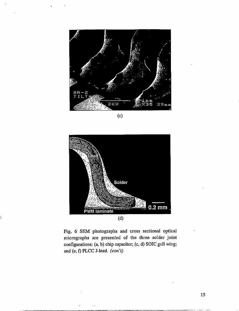
A comparison was made between the above observations and those developed
from similar test vehicles that were assembIed with 96.5Sn-3.5Ag or 58Bi-42Sn
so1ders[8]. Those prototypes were subjected to the same thermal cycling environments.
The Sn-Ag solder joints appeared very similar to those of the Sn-Ag-Bi interconnects
after 5000 cycles. On the other hand, the Bi-Sn solder joints rapidly degraded with
thermal cycling. This point is exemplified by the optical micrograph in Fig. 14 showing
an SOIC solder joint after 5000 thermal cycles. The mechanism by which the Bi-Sn joint
degraded is a result of the accelerated intermetallic compound layer growth at solder/Cu
interfaces[9]. In this case, that interface is that between the SOIC gull wing lead and the
Bi-Sn solder. Specifically, the Bi component of the solder does not participate in the
layer development. As a result, it is rejected ahead of the growing intermetallic
compound layer, forming a brittle, continuous layer ahead of the latter. Consequently,
the Bi layer readily fractures, producing voids as a result of the sample fabrication
process but more importantly, causing a significant drop in the strength of the interface.
Finally, there was no 10SSof electrical continuity in Sn-Ag-Bi solder joints after
the 5000 cycle duration.
10,000 thermal cycles
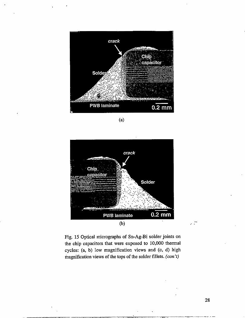
The chip capacitor Sn-Ag-Bi solder joints retained excellent integrity after 10,000
thermal cycles (Figs. 15a, 15b). The most persistent failure mode was that of crack
formation at the top of the solder fillet. The extent of the crack development was greater
than that observed after 5000 thermal cycles; a worse case is shown in Figs. 15c and 15d.
The surface profile of the fillets showed a slightly rougher appearance. In one case, a
crack had initiated at the rough, fillet surface and propagated about 75% of the distance
towards the termination. There was no appearance of deformation or cracking of the
solder in the gap between the capacitor and the bond pad. Also, there was no discemable
evolution by the microstructure when the images in Fig. 15 were compared with those of
chip capacitor solder joints in the as-fabricated condition.
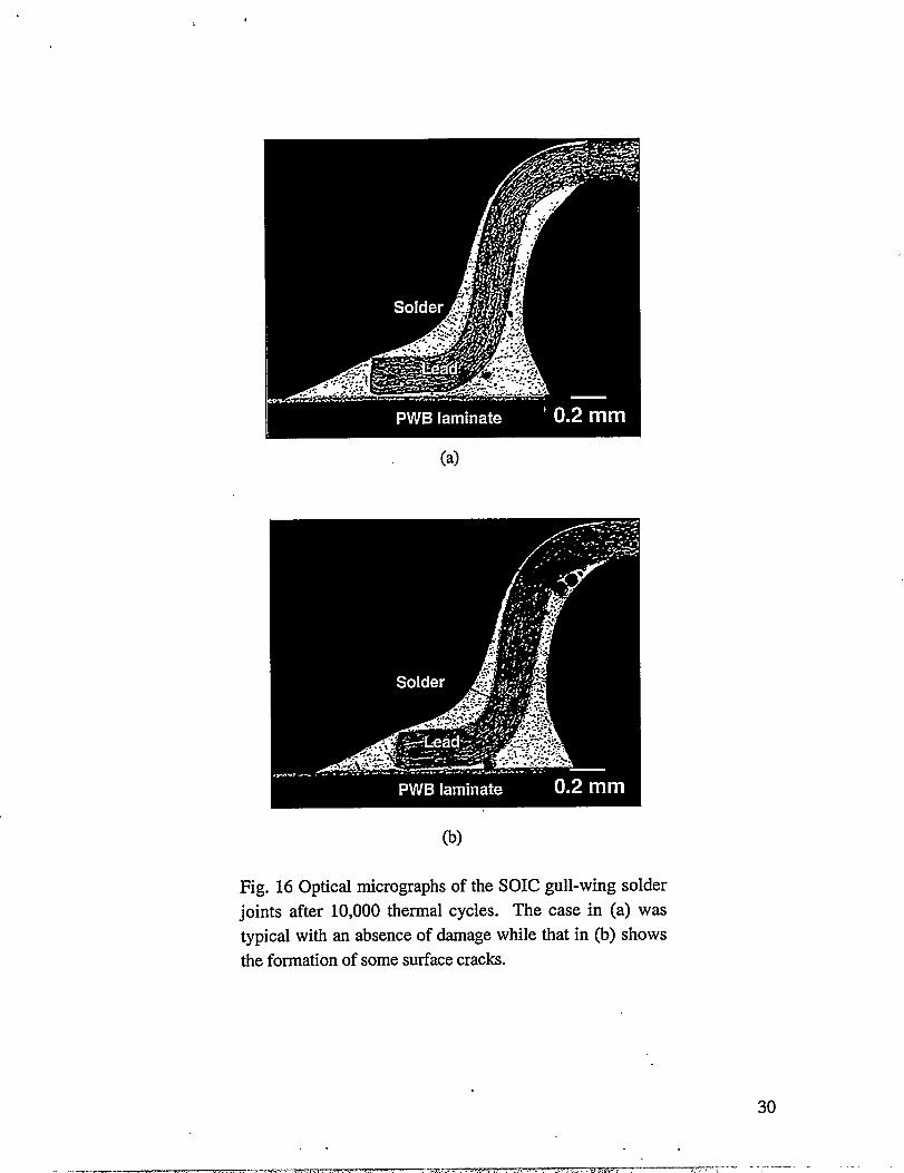
Damage to the SOIC solder joints was largely absent in the cases that were
examined (Fig. 16a). Some roughening of the fillet surfaces was observed. In the joint
shown in Fig. 16b, small cracks formed in the top surface solder film as well as on the
lower reaches of the fillet surface. However, those cracks did not extend to a degree that
would pose a significant threat to the functionality of the interconnect. There was no
indication of damage to the solder in the gap found between the lead and the bonding
pad. The general microstructure of the solder throughout the joint was not significantly
changed by the thermal cycling environment. . . .
6

The PLCC solder joints exhibited some damage. Shown in Figs. 17a and 17b are
low magnification micrographs of the solder joint cross sections. The solder fillet
surfaces have roughened with the cycling exposure. Cracks were observed on the thin
solder film coating the top of the leads. A crack was also noted in the heel fillet of the
joint shown in Fig. 17a. An improved view of the crack is shown in Fig. 17c which,
along with Fig. 17d, provide high magnification images of the heel fillets. The crack
does not appear to be associated with any microstructural inhomogeneity of the solder.
The location of the crack suggests that its source was global thermal expansion mismatch
between the package and laminate that resulted in bending (tensile) loads by the J-lead
and subsequent cracking in the fillet. Shear fatigue loads caused by both global and local
residual stresses had no observable effect on the Sn-Ag-Bi solder because in the gap
region at which such stresses were of maximum magnitude, no damage was observed in
the solder microstmcture. Only isolated areas of grain boundary slip within the Sri-rich
matrix were noted. ~
In summary, exposure of the chip capacitor solder joints, SOIC gull-wing lead
solder joints, and the PLCC J-lead solder joints to 10,000 thermal cycles did not degrade
the integrity of the solder joints to a degree that would jeopardize their functionality.
Clearly, the solder fillets incurred some crack damage which, in allbut a few instances,
remained as largely near-surface defects. There was no evidence of interracial failures
between the solder and the lead or bonding pad surfaces. Also, the Sn-Ag-Bi solder
microstructure appeared to be stable under the thermal cycling exposure by having shown
no distinguishable changes when compared to similar, as-fabricated solder joints. There
was no loss of electrical continuity in any of the joints.
Solder joint strength measurements
The shear strength values as a function of the number of thermal cycles for the
chip capacitor solder joints, are shown in Fig. 18. It is observed that the very high, as-
fabricated strength (Ocycles) of 135 N did not change significantly when the parts were
subjected to 1000 and 2500 thermal cycles. The mean strength began to decrease with
5000 and 10,000 cycles. It should be noted that the strength level after 10,000 cycles, 92
N, is higher than that of similar Sn-Pb solder joints without thermal cycling (87 N).
Therefore, the Sn-Ag-Bi chip capacitor solder joints retained adequate strength after
10,000 thermal cycles.
Although the mean strength values were affected by the thermal cycling
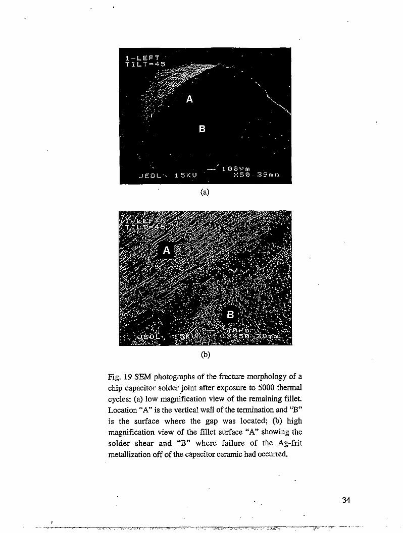
condhions, the fracture morphology was not sensitive to the range of cycles. An SEM
photograph of a failed solder joint from the test vehicle exposed to 5000 cycles is shownin Fig. 19; it is representative of all of the shear tested capacitors, from the as-fabricated
condition to the 10,000 cycle condition. A low magnification view in Fig. 19a shows that
the solder fillet remained intact with no apparent darnage to it beyond the immediate
7
. .
... , ,. .,. =YGvz_=,.. , ... .. . “.-. . . . . . . . .. . . . . 7 ,.., ,,, ,.,...! ,. , .,,... .% , ~ ,--$~,.+.,.,

#
vicinity of the fracture. The high magnification image in Fig. 19b shows the differing
morphologies between the vertical wall (“A”) of the fillet and the “floor,” the latter being
the gap region between the chip and the bonding pad (“B”). Fracture along surface “A”
had propagated in the solder, very close to its interface with the chip termination. The
solder sheared in a relatively ductile manner as is evidenced by an absence of small
cracks. The surface morphology representing the gap region (“B”) was caused by
fracture between the Ag-based, thick film metallization (or “frit”) and the ceramic body
of the chip capacitor. That is, the strength of the solder in joint’s gap exceeded that of the
capacitor structure. This trend was not unexpected. The gap geometry imposes a
constraint on deformation from occurring in the solder. Therefore, the solder appears to
be stronger in the gap than it is in regions of little or no constraint, such as the fillet. In
the gap region, the strength of the Sn-Ag-Bi solder exceeded that of the capacitor
structure, causing failure at the metallizatiordceramic interface.
The shear strength (Fig. 18) and fracture morphology information (Fig. 19) can be
correlated as follows. As noted above, the fracture path propagated in both the solder and
the chip capacitor structure over the range of thermal cycle conditions. The shear
strength exhibited a decline at 5000 and 10,000 cycles. Assuming that the adhesion
strength between the metallization and the capacitor was not affected by the thermal
cycling conditions, then the drop in strength was due to a decrease in load-bearing area at
the solder/termination interface (top of region “A”). Further growth of the fillet tip
cracks shown in Figs. 11 (5000 thermal cycles) and 15 (10,000 thermal cycles) was the
likely cause for the drop in shear strength of the solder joints.
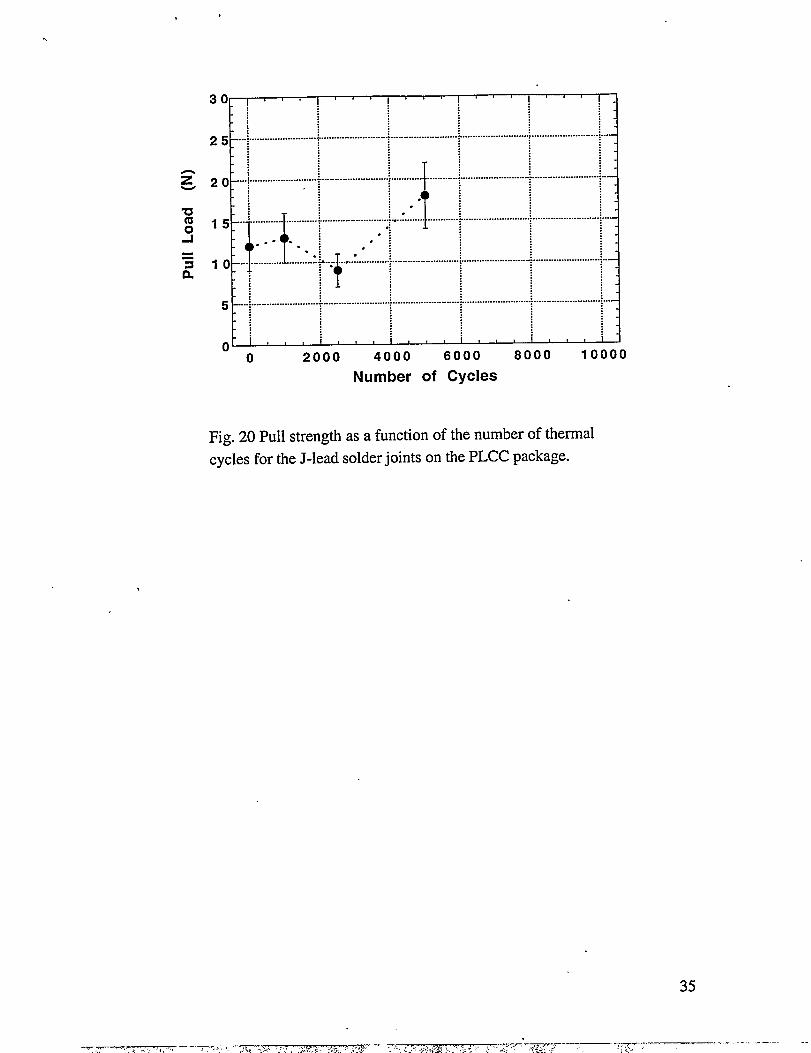
The pull strength of the J-leads on the 68 I/O PLCC packages was determined as a
function of thermal cycling; those data appear in Fig. 20. No pull tests were performed
on the J-leads of PLCC packages exposed to 10,000 thermal cycles. The data show that
the cycling environment had no consistent effect on the solder joint strength. Therefore,
the surface and fillet cracks observed in the metallographic cross sections appear to have
been inconsequential to the overall mechanical integrity of the J-lead solder joints. The
strength levels in Fig. 20 can be compared against that for similar solder joints made with
the traditional Sn-Pb solder- 12 N (as-fabricated condition). Therefore, the Sn-Ag-Bi
solder retained strength levels that are comparable with those of Sn-Pb solder, even after
the former has been thermally cycled.
The reason that the J-lead pull strengths of solder joints made with inherently
stronger Sn-Ag-Bi are comparable to, rather than higher than, the pull strengths of similar
Sn-Pb solder joints is due to the test configuration. Pulling the lead from the substrate
surface places the solder joint structure in primarily a tensile stress mode. The
deformation/fracture process becomes more sensitive to interfaces that are perpendicular
to the applied load that it would be if tested in shear. The interface structures of Sn-Ag-
8
~—,m .—— ..—.

,
Bi and Sn-Pb solder joints are nearly identical in composition (Cu$ns) and thickness.
Therefore, the Sn-Ag-Bi and Sn-Pb soldered J-leads exhibited similar failure strengths.
Summary. .
1. An evaluation was performed which examined the aging of surface mount solder joints
made with 91.84Sn-3.33Ag-4.83Bi bearing solder. Defect analysis of the as-fabricated
test vehicles revealed excellent solderability, good package alignment, and a minimum
of voids, all properties that allowed the prototypes to serve as suitable test vehicles for a
thermal cycling (O°C- 100°C) reliability assessment.
2. Continuous DC electrical monitoring of the solder joints did not reveal any opens for
any of the test conditions through 10,000 cycles.
3. The solder joints exhibited no significant degradation through 2500 cycles. This
observation is based upon: (a) an absence of microstructural damage in the way of
deformation or crack formation in the joint and (b) sustained shear and pull strengths of
chip capacitors and J-leaded solder joints, respectively.
4. Thermal cycles of 5000 and 10,000 caused some surface cracking of the solder joints,
and in a few cases, deeper cracks in thinner reaches of a few solder fillets. However, the
crack morphologies dld not have the same characteristics as do those which indicate
substantial thermal mechanical fatigue damage in Sn-Pb solders. That is, there was no
deformation or cracking in the solder located in the gap between the package I/O and the
circuit board pad nor in the interior of the fillets, both locations that would raise concerns
of joint mechanical integrity. A drop in the chip capacitor shear strength was attributed .
to further growth of a crack that traditionally develops at the top-most tip of the fillet.
References[1] US Patent No. 5,439,639, “Tin-Silver Bismuth Solders for Electronics Assembly,”
1994, Sandia National Laboratories, Albuquerque, NM. -
[2] I. Artaki, A. Jackson, and P. Vianco, “Fine Pitch Surface Mount Assembly with Lead-
Free, Low Residue Solder Paste,” Proc. Su#ace Mount Zntemational (1994).
[3]P. Vianco and P. Mizik, “Prototyping Lead Free Solders on Hand-Soldered, Through-
Hole Circuit Boards,” Proc. SAMPE Conference (1994).
9
--- ,= -~.-~~. ... - , .... , ,-k.~q”. ., .. ;,, . . . . , ....,,V,. . .. . . --.:. ,, . . .. . . . . . . . . ,., ,. ... . . ...T ..— ..—:=. ., -,..’

[4] P. Vianco, J. Rejent, I. Artaki, U. Ray, D. Finley, and A. Jackson, “Compatibility of
Lead-Free Solders with Lead Containing Surface Finishes as a Reliability Issue in
Electronic Assemblies,” Proc. ECTC Conference (1996).
[5] P. Vianco and C. May, “An Evaluation of Prototype Surface Mount Circuit Boards
Assembled with Three Non-Lead Bearing Solders,” Proc. Surface Mount International
(1995).
[6]P. Vianco and J. Rejent, “Prototype Circuit Boards Assembled with Non-Lead
Bearing Solders,” Proc. PRICM-3 Conference (1998).
[7] P. Vianco and J. Rejent, “Properties of Ternary Sn-Ag-Bi Solder Alloys: Part I -
Thermal Properties and Microstructural Analysis, and Part II- Nettability and
Mechanical Properties Analyses,” to be published in J. of Electronic Materials, (1999).
[8] P. Vianco, I. Artaki, and A. Jackson, “Assembly Feasibility and Reliability Studies of
Surface Mount Circuit Boards Manufactured with Lead-Free Solders,” Proc. Su~ace
Mount Intern., (1994).
[9]P. Vianco, A. Kilgo, and R. Grant, “Interrnetallic Compound Layer Growth by Solid-
State Reactions Between 58Bi-42Sn Solder and Copper,” J. Elect.Mater.M (1995)3P.
1493.
10
—,, , ,., .-, -Ty.m :... ,, . ,.-,., , $, . . . . . . . . . . . . . . . . . . . . . !) ~—--z!m > —-—.—

#
Fig. 1 SEM photograph of the microstmcture of the Sn-Ag-
Bi alloy.
Fig. 2 TEM micrograph of the Sn-Ag-Bi solder
microstructure showing boundary pinning by the Bi
particles.
. 11
-.---r— -m . . . . . . . . . .. .. . . . .-.. .=. —..

r ..
Fig. 3 Photograph of the prototype circuit board used to
evaluate the reliability of surface mount, Sn-Ag-Bi solder
joints.
t
Force
E:..~:~:fi~..;:::::::::::j:::::::::::::::...................:
‘o-?.+:.:.:.:.:+:.fi;;~::flx :::“::=.:i: m.?......................
I
L
:. .:;J:+:.. . . . . . . . ..::%.
.:- . . . . . . . . . . . . . . . . . . . . .
Chip oapacitor J-leadshear test pull test
(a) (b)
Fig. 4 Schematic diagrams of the mechanical testing modes
used to evaluate the solder joints from (a) the leadless chip
capacitor solder joints and (b) the J-leaded, PLCC package.
.
<
12
—. -.. .— ------ -------- y
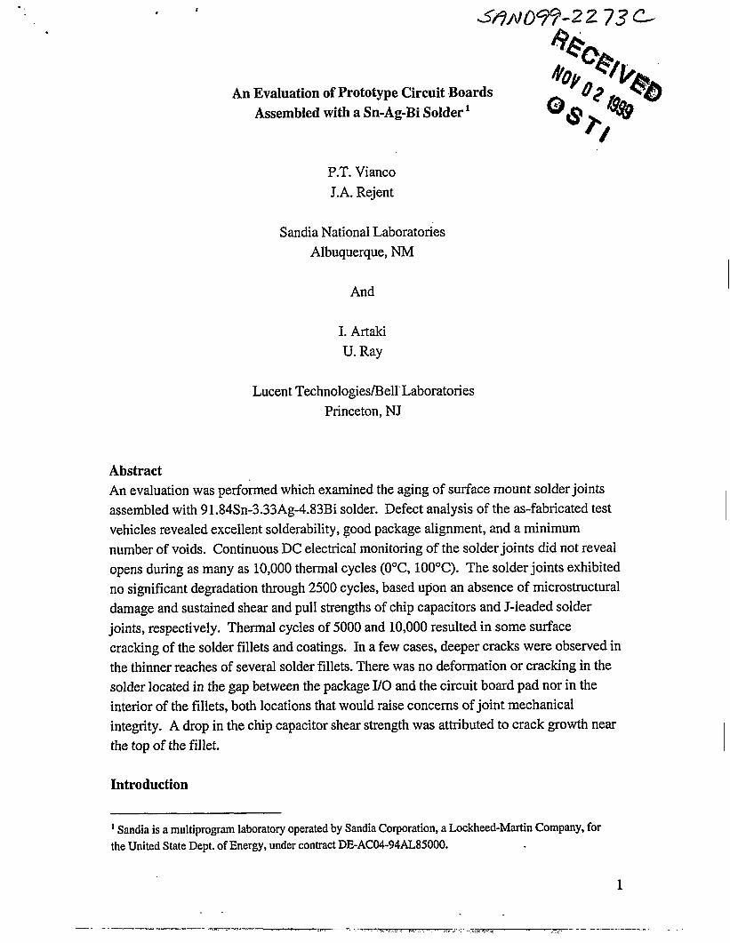
(a) ‘
(b)
(c)
Fig. 5 Photographs of views of each of the package types
onthetest vehicle after assembly: (a) chip capacitors, (b)
SOIC, and (c) PLCC.
13
-- . .J-m . .—. ..--— — .

.
(a)
14
. ..-,— — ,—-.. ,..... .... , -.9.- ,.,. .— -.—-——
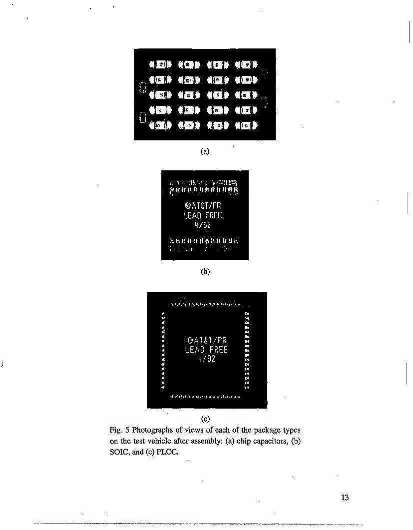
Fig. 6 SEM photographs and cross sectional optical
micrographs are presented of the three solder joint
configurations: (a, b) chip capacito~ (c, d) SOIC gull wing;
and (e, f) PLCC J-lead. (con ‘t)
.
(c)
(d)
Fig. 6 SEM photographs and cross sectional optical
micrographs are presented of the three solder joint
configurations: (a, b) chip capacitou (c, d) SOIC gull wing;
and (e, f) PLCC J-lead. (con ‘t)
15
— —-. -.=-

.
(e)
(f)
Fig. 6 SEM photographs and
micrographs are presented of
cross sectional optical
the three solder joint
configurations: (a, b) chip capacitou (c, d) SOIC gull wing;
and (e, f) PLCC J-lead.
16
?--?-m ,. <... .4.VT: T.-7- .. >.’, +. .,.....—. . . . . . . -
- 7., . ...,. ,,,., ,. , , . . . . . .. . . . . . , . . . c . . . . . . . . . . . ..+ />,. <.. , ,, .-.,

(a)
Fig. 7 Optical micrographs of a J-lead joint from a PLCC
package after 1000 thermal cycles: (a) low magnification
view of the whole joint and (b) high magnification view of
the heel fillet.
17
.
.. . . ... .-.Z? . . ., . . . . . . . . . . . . . . . . . . . . . . . . .~ ,—: .._ .- ..— -.—-
. . . , . . mm. .7

(a)
“ @)
Fig. 8 (a) Chip capacitor solder joint after 2500 thermal
cycles. (b) High magnification image of the crack formed
at the top of the fillet.
. 18
... T-. ,, . .._ . . . . . . . ,. -m,—-— .-.. -—_—
., .,.. . -7=----- . . . ?,. , ..

#
(a)
19.
.—. >,., , --- .. V.=.- .. ,.,,.. ,.-,,,,,, ---- ,...,!.,. ..!, ).~,--.-* --——T -.— ——.. - . . . ..,.
Fig.9 (a) SOIC solder joint after 2500 thermal cycles. (b).High magnification image of thegapregion between the
gull-wing lead and circuit board pad.

(a)
Fig. 10 (a) PLCC solder joint after 2500 thermal cycles. (b)
High magnification image of the gap region between the J-
lead and circuit board pad.
20
-——— — --.,— .-. --..m---- ~— -- —— .— -

.
(a)
(b)
Fig. 11 Chip capacitor solder joint after 5000 thermal
cycles: (a) SEM image of the solder fillet, (b) optical
micrograph showing the cross section of chip capacitor
joint, and (c) high magnification, optical rnicrograph of the
gap region of the solder joint. (con’t)
21
. .
. --- .—.= ~ ,, ,,.~+-,v,-. *, -“ —.— —-.
-,7 -..-,. . ,..,

.
(c)
Fig. 11 Chip capacitor solder joint after 5000 thermal
cycles: (a) SEM image of the solder fillet, (b) optical
micrograph showing the cross section of chip capacitor
joint, and (c) high magnification, optical micrograph
showing the gap region of the solder joint.
22
-- ?, ?,...,., . ..$-. -:~.-”~. ..,,,, . ,r,. ., .. . . . . ... . . . . ,- ..’,-.— ?,~~ ~::_- . . . . . . . . . .
. . . ..”...... . . . . . . -., .,,

(a)
1
Fig. 12 SOIC solder joint after 5000 thermal cycles: (a, b)
SEM images of the solder fillet, (c) optical micrograph
showing the cross section of gull-wing lead joint, and (d)
high magnification, optical micrograph showing the gap
region of the solder joint. (con ‘t)

(c)
24
— ——...
(d)
Fig. 12 SOIC solder joint after 5000 thermal cycles: (a, b)
SEM images of the solder fillet, (c) optical micrograph
showing the cross section of gull-wing lead joint, and (d)
high magnification, optical micrograph showing the gap
region of the solder joint.

(a)
Fig. 13 PLCC solder joint after 5000 thermal cycles: (a)
SEM image of the solder fillet, (b) optical micrograph
showing the cross section of J-lead joint, (c) high
magnification, optical micrograph showing cracks in the
solder film on the lead surface, and (d) optical micrograph
of solder in the gap region of the joint beneath the lead.
(con’t)
25
.. . . ,,.-..,,.!. ,, .,,.+pgy.~-. . . . ..\ ,, ,, -~~,
., . .. . . . .,* 3.,. . . .

(c)
(d)
Fig. 13 PLCC solder joint after 5000 thermal cycles: (a)
SEM image of the solder fillet, (b) optical micrograph
showing the cross section of J-lead joint, (c) high
magnification, ,optical micrograph showing cracks in the
solder film on the lead surface, and (d) optical micrograph
of solder in the gap region of the joint beneath the lead.
26.
———-—— —.-—, . --., ... ,. . -7— -.
Fig. 14 Optical micrograph of the a 58Bi-42Sn, SOIC
solder joint after 5000 cycles. Severe
taken place.
deterioration has
27
------ ,-.-77.7----- ,L_- —---- --- .
(a)
Fig. 150ptical micrographs of Sn-Ag-Bi solder jointson
the chip capacitors that were exposed to 10,000 thermal
cycles: (a, b) low magnification views and (c, d) high
magnification views of the tops of the solder fillets. (con ‘t)
-... .
28
— .. —.—- ..m=—

(c)
29
-— ,.---,. .. ..., ,..,. .. ... - ..’..... :..’>. ,,, -.—?%?,>:,. —,.——- .—.——. .... ..—..% .
(d)
Fig. 15 Optical micrographs of Sn-Ag-Bi solder joints on
the chip capacitors that were exposed to 10,000 thermal
cycles: (a, b) low magnification views and (c, d) high
magnification views of the tops of the solder fillets.
(a)
. .
——. .“.. ,. ,., .~., . .. >...,, ,---.,. ,-7 —..,. . . . ..— — . .
Fig. 16 Optical micrographs of the SOIC gull-wing solder
joints after 10,000 thermal cycles. The case in (a) was
typical with an absence of damage while that in (b) shows
the formation of some surface cracks.
30

.
(a)
Fig. 17 Optical micrographs of the PLCC J-lead solder
joints after 10,000 thermal cycles: (a, b) low magnification
images and (c, d) high magnification images of the solder
joint fillets. (con’t)
. .

,
(c)
(d)
Fig. 17 Optical micrographs of the PLCC J-lead solder
joints after 10,000 thermal cycles: (a, b) low magnification
images and (c, d) high magnification images of the solder
joint fillets.
32
#/

,
714
6
4
:~1~~~:.
0 .... ............. .................... ....................{...........................~ ................................-. ----- . . .. .
. .. .
0 -...+ . . . . . . . . ~. ,:
~1~~ ‘~..------:-....................y----------.......-...-.......-7 ................... -----y“.;.
-. .::.. -;-. .
(J -...:
~:
. . . . . . . . . . . . . . . . . . . . . . . . . . . . . . . . . . . . . . . . . . . . . . . . . . . . . . . . . . . . . . . . . . . . . . . . . . . . . . . . . ...+.... . . . . . . . . . . . . . . . . . . . . . . .. . . . . . . . . . . . . . . . . . . . . . .... ...:...
-.. .
0 - ................... ............ ............................. ..........................~ ...
0 -;......................................................................................... ........................... ...............................—
o I I I I I I
o 2000 4000 6000 8000 10000
Number of Cycles
Fig. 18 Shear strength as a function of the number of
thermal cycles for the chip capacitor solder joints.
.-= — -=;> ~_c-. . . . . . . ,,, .,. ,,. ,.. ... n .,, .., . .. . .. . -., .!. rT:w .-_— . . . . .
,* T-
. #
(a)
t—–—7——
Fig. 19 SEM photographs of the fracture morphology of a
chip capacitor solder joint after exposure to 5000 thermal
cycles: (a) low magnification view of the remaining fillet.
Location “A” is the vertical waI1of the termination and “B”
is the surface where the gap was located; (b) high
magnification view of the fillet surface “A” showing the
solder shear and “B” where failure of the Ag-frit
metallization off of the capacitor ceramic had occurred.
34
. .
,,.,, .~~fi-m.. <,,., ,,, ., . . . ....7 ,. .,,, . ,,,. -K= . . .2.. -,..,, , ., .-. ., .,, . . . . . . .. . . --..-+.*>.,,.,——.
, <-...,,,. . . ,,* -_ —-. —----
30 I ! ! I
5 ::............................... ..................................... ..........................................
o -:, :
q!
............................... ....................................... ............~ .......
:.;.
5 ““:-“””””””--””“..-””””””.”-””-.””””””””--.”””””:.-”:”””””””.“”””””””...!””””-..””””””””-----”’
:f{:
.. -.: .;. .:. .:
,!
.0 ... ............ ...........~: .......................................................... ..............
5L. ...~......".................... .......""........."......~""""........."".."...."""".. ........"..".........".
n I I I I
-.r,--- ——., -’ .,,.,.,. ,,$
, q,-, --m -. — .;+ ,:. ,+=<.-=- ~,.,.* .,,.>, .,. .
_T~--. ----~ .-– --
-)., . ... .,.% ‘- 7 ?) .. ,-- ,: ..: .,..!< ~. ~ .:, . . -., ,; ,.. . , ,- . ..
I
.......................-----
............................-
...........................—
............................-
........................:.. -
I
“o 2000 4000 6000 8000 10000
Number of Cycles
Fig. 20 Pull strength as a function of the number of thermal
cycles for the J-lead solder joints on the PLCC package.
35


