
SCLK
DOUT
DIN
Control and Serial Interface
GNDAVSS
DRDY
AVDD
VNCP
XTAL1/CLKIN
CS
Negative Charge Pump
Voltage Reference
AD
S13
1A04
Onl
y
Reference Mux
REFEXT IOVDD
CLK/XTALXTAL2
M[2:0]
RESET
DONE
'6 ADC
'6 ADC
'6 ADC
'6 ADC
AIN4N
AIN4P
AIN3N
AIN3P
AIN2N
AIN2P
AIN1N
AIN1P
REFNREFP
Out-of-Range Detect
Data Integrity
WatchdogTimer
Product
Folder
Order
Now
Technical
Documents
Tools &
Software
Support &Community
An IMPORTANT NOTICE at the end of this data sheet addresses availability, warranty, changes, use in safety-critical applications,intellectual property matters and other important disclaimers. PRODUCTION DATA.
ADS131A02, ADS131A04SBAS590D –MARCH 2016–REVISED JANUARY 2018
ADS131A0x 2- or 4-Channel, 24-Bit, 128-kSPS, Simultaneous-Sampling, Delta-Sigma ADC
1
1 Features1• 2 or 4 Simultaneous-Sampling Differential Inputs• Data Rates Up to 128 kSPS• High Performance:
– Single-Channel Accuracy: Better Than 0.1% at10,000:1 Dynamic Range
– Effective Resolution: 20.6 Bits at 8 kSPS– THD: –100 dB at 50 Hz and 60 Hz
• Integrated Negative Charge Pump AllowsAbsolute Input Voltages Below Ground
• Flexible Analog Power-Supply Operation:– Using Negative Charge Pump: 3.0 V to 3.45 V– Unipolar Supply: 3.3 V to 5.5 V– Bipolar Supply: ±2.5 V
• Digital Supply: 1.65 V to 3.6 V• Low-Drift Internal Voltage Reference: 6 ppm/°C• ADC Self Checks• Cyclic Redundancy Check (CRC) and Hamming
Code Error Correction on Communications• Multiple SPI Data Interface Modes:
– Asynchronous Interrupt– Synchronous Master and Slave
• Package: 32-Pin TQFP• Operating Temperature Range:
–40°C to +125°C
2 Applications• Power Protection: Circuit Breakers, Relay
Protection• Energy Metering: Single Phase, Polyphase,
Power Quality• Test and Measurement• Battery Test Systems• Data Acquisition Systems
3 DescriptionThe ADS131A02 and ADS131A04 devices are two-and four-channel, simultaneous-sampling, 24-bit,delta-sigma (ΔΣ), analog-to-digital converters (ADCs).The wide dynamic range, with scalable data rates upto 128 kSPS, and internal fault monitors make theADS131A02 or ADS131A04 a good choice whendesigning for energy monitoring, grid protection, andcontrol applications. The ADC inputs can beindependently and directly interfaced to a resistor-divider network, a current transformer, or a Rogowskicoil to measure voltage or current. Flexible power-supply options, including an internal negative chargepump, are available to maximize the effectiveresolution for high dynamic range applications.
Asynchronous and synchronous master and slaveinterface options are available, providing ADCconfiguration flexibility when chaining multiple devicesin a single system. Several interface checks, ADCstartup checks, and data integrity checks can beenabled on the interface to report errors in the ADCand during data transfer.
The complete analog front-end (AFE) solutions arepackaged in a 32-pin TQFP package and arespecified over the industrial temperature range of–40°C to +125°C.
Device Information(1)
PART NUMBER PACKAGE BODY SIZE (NOM)ADS131A0x TQFP (32) 5.00 mm × 5.00 mm
(1) For all available packages, see the orderable addendum atthe end of the data sheet.
Simplified Block Diagram

2
ADS131A02, ADS131A04SBAS590D –MARCH 2016–REVISED JANUARY 2018 www.ti.com
Product Folder Links: ADS131A02 ADS131A04
Submit Documentation Feedback Copyright © 2016–2018, Texas Instruments Incorporated
Table of Contents1 Features .................................................................. 12 Applications ........................................................... 13 Description ............................................................. 14 Revision History..................................................... 25 Device Comparison Table ..................................... 56 Pin Configuration and Functions ......................... 57 Specifications......................................................... 7
7.1 Absolute Maximum Ratings ...................................... 77.2 ESD Ratings.............................................................. 77.3 Recommended Operating Conditions....................... 87.4 Thermal Information .................................................. 87.5 Electrical Characteristics........................................... 97.6 Timing Requirements: Asynchronous Interrupt
Interface Mode ......................................................... 127.7 Switching Characteristics: Asynchronous Interrupt
Interface Mode ......................................................... 127.8 Timing Requirements: Synchronous Master Interface
Mode ........................................................................ 137.9 Switching Characteristics: Synchronous Master
Interface Mode ......................................................... 137.10 Timing Requirements: Synchronous Slave Interface
Mode ........................................................................ 147.11 Switching Characteristics: Synchronous Slave
Interface Mode ......................................................... 147.12 Typical Characteristics .......................................... 17
8 Parameter Measurement Information ................ 228.1 Noise Measurements .............................................. 22
9 Detailed Description ............................................ 259.1 Overview ................................................................. 25
9.2 Functional Block Diagram ....................................... 259.3 Feature Description................................................. 269.4 Device Functional Modes........................................ 349.5 Programming........................................................... 369.6 Register Maps ........................................................ 55
10 Application and Implementation........................ 6710.1 Application Information.......................................... 6710.2 Typical Application ................................................ 7410.3 Do's and Don'ts..................................................... 7610.4 Initialization Set Up .............................................. 78
11 Power Supply Recommendations ..................... 8011.1 Negative Charge Pump......................................... 8011.2 Internal Digital LDO............................................... 8011.3 Power-Supply Sequencing.................................... 8011.4 Power-Supply Decoupling..................................... 81
12 Layout................................................................... 8212.1 Layout Guidelines ................................................. 8212.2 Layout Example .................................................... 83
13 Device and Documentation Support ................. 8413.1 Documentation Support ....................................... 8413.2 Related Links ........................................................ 8413.3 Receiving Notification of Documentation Updates 8413.4 Community Resources.......................................... 8413.5 Trademarks ........................................................... 8413.6 Electrostatic Discharge Caution............................ 8413.7 Glossary ................................................................ 84
14 Mechanical, Packaging, and OrderableInformation ........................................................... 85
4 Revision HistoryNOTE: Page numbers for previous revisions may differ from page numbers in the current version.
Changes from Revision C (November 2016) to Revision D Page
• Changed document title from 2- or 4-Channel, 24-Bit, Simultaneously-Sampling, Delta-Sigma ADC to 2- or 4-Channel, 24-Bit, 128-kSPS, Simultaneous-Sampling, Delta-Sigma ADC .............................................................................. 1
• Changed VAVDD to AVDD, VAVSS to AVSS, VGND to GND, and VIOVDD to IOVDD throughout document ................................ 1• Changed Features section .................................................................................................................................................... 1• Changed Description section.................................................................................................................................................. 1• Deleted footnote 2 ................................................................................................................................................................. 6• Changed AVDD, AVSS, VNCP, and XTAL2 pin descriptions and footnote 1 for clarity ....................................................... 6• Changed CAP to GND Power supply voltage parameter specifications from GND – 0.3 V to 0.3 V for the minimum
specification and from GND + 2.0 V to 2.0 V for the maximum specification ........................................................................ 7• Changed Analog input voltage parameter descriptions from REFEXT to AVDD to REFEXT and from REFN input to
AVSS to REFN ....................................................................................................................................................................... 7• Changed Digital input voltage parameter description to include the names of the digital input pins ..................................... 7• Deleted CMRR footnote from Recommended Operating Conditions table ............................................................................ 8• Added symbol to Reference input voltage parameter ............................................................................................................ 8• Changed Offset drift parameter typical specification from 1.2 µV/°C to 2.5 µV/°C and maximum specification from 3
µV/°C to 4 µV/°C..................................................................................................................................................................... 9• Changed Gain drift parameter typical specification from 0.25 ppm/°C to 0.5 ppm/°C .......................................................... 9• Deleted separate AVDD PSRR specification for the ADS131A02 ........................................................................................ 9

3
ADS131A02, ADS131A04www.ti.com SBAS590D –MARCH 2016–REVISED JANUARY 2018
Product Folder Links: ADS131A02 ADS131A04
Submit Documentation FeedbackCopyright © 2016–2018, Texas Instruments Incorporated
Revision History (continued)• Changed Reference buffer offset parameter typical specification from 170 µV to 250 µV .................................................... 9• Changed Reference buffer offset drift parameter typical specification from 1.1 µV/°C to 4 µV/°C and maximum
specification from 4.3 µV/°C to 7 µV/°C ................................................................................................................................. 9• Changed Temperature drift parameter typical specification from 4 ppm/°C to 6 ppm/°C .................................................... 10• Deleted VNCP parameter minimum specification and changed typical specification from –1.95 V to –2 V........................ 10• Changed Electrical Characteristics table so all Power-Supply subsections are condensed to one Power-Supply
subsection............................................................................................................................................................................. 10• Changed free-air to ambient in condition statements of Timing Requirements tables......................................................... 12• Changed location of several interface timing parameters to the Timing Requirements and Switching Characteristics
tables from the Detailed Description section ....................................................................................................................... 12• Changed unit from ns to tCLKIN in tc(SC) and tw(SCHL) rows of Timing Requirements: Synchronous Master Interface
Mode table ............................................................................................................................................................................ 13• Added DRDY Synchronization Timing for Synchronous Slave Mode (CLKSRC = 0) to RESET Pin and Command
Timing figures ....................................................................................................................................................................... 16• Changed Clock section for clarification and changed setting of XTAL2 pin ........................................................................ 26• Changed Clock Mode Configurations figure to include load capacitors for clarity ............................................................... 27• Changed Analog Input section for clarity.............................................................................................................................. 28• Changed Equivalent Analog Input Circuitry figure................................................................................................................ 28• Changed Input Overrange and Underrange Detection section for clarity ............................................................................ 30• Changed location of Reference section .............................................................................................................................. 30• Changed External Reference Driver figure........................................................................................................................... 31• Changed Internal Reference figure ..................................................................................................................................... 31• Changed Digital Decimation Filter section for clarity............................................................................................................ 32• Deleted figure and table from Reset (RESET) section......................................................................................................... 35• Changed Fixed versus Dynamic-Frame Mode section for clarity......................................................................................... 36• Added Cyclic Redundancy Check (CRC) section for clarity................................................................................................. 39• Changed CRC with CRC_MODE = 0 and CRC Using the WREGS Command figures to using red shading instead of
//Zero .................................................................................................................................................................................... 39• Changed Data Ready (DRDY) section for clarity ................................................................................................................. 43• Changed pulldown to pullup in bulleted list of ADC Frame Complete (DONE) section ...................................................... 47• Changed description of UNLOCK from POR or RESET section.......................................................................................... 52• Changed description of RREG: Read a Single Register section ......................................................................................... 52• Changed number of registers written plus one (n+1) to number of registers written minus one in WREGS: Write
Multiple Registers section..................................................................................................................................................... 54• Changed User Register Description section for clarity......................................................................................................... 56• Changed Unused Inputs and Outputs section for clarity...................................................................................................... 67• Changed title of Multiple Device Configuration section and changed description for clarity ............................................... 68• Changed first paragraph of First Device Configured in Asynchronous Interrupt Mode to condense data from last
three paragraphs into one ................................................................................................................................................... 68• Changed description of First Device Configured in Synchronous Master Mode section to condense all paragraphs
into one................................................................................................................................................................................. 70• Changed description of All Devices Configured in Synchronous Slave Mode section to condense all paragraphs into
one ....................................................................................................................................................................................... 72• Changed ADS131A0x Configuration Sequence figure......................................................................................................... 79• Changed GND to AVSS in VNCP pin description of Negative Charge Pump section......................................................... 80• Changed title of Internal Digital LDO section ....................................................................................................................... 80• Changed description of Power-Supply Sequencing section................................................................................................. 80• Changed Bipolar Analog Power Supply to Unipolar Analog Power Supply with Negative Charge Pump Enabled figures. 81

4
ADS131A02, ADS131A04SBAS590D –MARCH 2016–REVISED JANUARY 2018 www.ti.com
Product Folder Links: ADS131A02 ADS131A04
Submit Documentation Feedback Copyright © 2016–2018, Texas Instruments Incorporated
Revision History (continued)• Changed first sentence of Layout Example section ............................................................................................................. 83• Changed ADS131A0x Layout Example figure to improve layout ......................................................................................... 83
Changes from Revision B (September 2016) to Revision C Page
• Changed document title from Analog Front-Ends for Power Monitoring, Control, and Protection to Simultaneously-Sampling, Delta-Sigma ADC .................................................................................................................................................. 1
• Changed ENOB to Effective Resolution in second sub-bullet of Noise Performance Features bullet................................... 1• Changed effective number of bits to effective resolution in Description section ................................................................... 1• Changed format of Absolute Maximum Ratings table; specification values did not change.................................................. 7• Changed title of Multiple Device Effective Resolution Histogram figure .............................................................................. 17• Changed Noise Measurements section ............................................................................................................................... 22
Changes from Revision A (March 2016) to Revision B Page
• Released ADS131A02 to production...................................................................................................................................... 1• Changed AC Performance, PSRR, THD, and SFDR parameters in Electrical Characteristics table: added rows for
ADS131A02 and added ADS131A04 to rows specific to that device ................................................................................... 9• Changed title of Figure 31 and Figure 32: added ADS131A04 ........................................................................................... 20• Added Figure 33 and Figure 34 ........................................................................................................................................... 21• Changed Noise Measurements section: changed Equation 1, Equation 2, Table 1, and Table 3 ...................................... 22• Added footnote to Figure 43 ................................................................................................................................................ 31• Changed R2 and R3 values in footnote of Figure 44 .......................................................................................................... 31• Changed Cyclic Redundancy Check (CRC) section ............................................................................................................ 39• Changed description of M2 pin functionality in Hamming Code Error Correction section ................................................... 40• Changed description of M0 pin functionality in SPI Interface section .................................................................................. 42• Changed first command status response value in RREGS: Read Multiple Registers section............................................. 52• Changed Table 15: changed register bits of row 00h, default setting and register bits of row 01h, and changed bits
2-0 of 11h, 12h, 13h, and 14h rows .................................................................................................................................... 55• Changed ID_MSB: ID Control Register MSB and ID_LSB: ID Control Register LSB registers ........................................... 56• Changed bits 2-0 of all ADCx: ADC Channel Digital Gain Configuration Registers ............................................................ 66
Changes from Original (March 2016) to Revision A Page
• Released ADS131A04 to production ..................................................................................................................................... 1

ADS131A04
2526272829303132
1
2
3
4
5
6
7
8
9 10 11 12 13 14 1615
17
18
19
20
21
22
23
24
XT
AL1
/ C
LKIN
XT
AL2
M0
M1
M2
GN
D
IOV
DD
CA
P
NC
CS
SCLK
DOUT
DIN
DRDY
AIN1N
AIN1P
AIN2N
AIN2P
AIN3N
AIN3P
AIN4N
AV
SS
VN
CP
AV
DD
AIN4P
RE
FP
RE
FN
RE
FE
XT
IOV
DD
RESET
DONE
RE
SV
ADS131A02
2526272829303132
1
2
3
4
5
6
7
8
9 10 11 12 13 14 1615
17
18
19
20
21
22
23
24
XT
AL1
/ C
LKIN
XT
AL2
M0
M1
M2
GN
D
IOV
DD
CA
P
NC
CS
SCLK
DOUT
DIN
DRDY
AIN1N
AIN1P
AIN2N
AIN2P
NC
NC
NC
AV
SS
VN
CP
AV
DD
NC
RE
FP
RE
FN
RE
FE
XT
IOV
DD
RESET
DONE
RE
SV
5
ADS131A02, ADS131A04www.ti.com SBAS590D –MARCH 2016–REVISED JANUARY 2018
Product Folder Links: ADS131A02 ADS131A04
Submit Documentation FeedbackCopyright © 2016–2018, Texas Instruments Incorporated
5 Device Comparison Table
PRODUCT NO. OF ADC CHANNELS MAXIMUM SAMPLE RATE (kSPS)ADS131A02 2 128ADS131A04 4 128
6 Pin Configuration and Functions
ADS131A02: PBS Package32-Pin TQFP
Top View
ADS131A04: PBS Package32-Pin TQFP
Top View
(1) See the Unused Inputs and Outputs section for unused pin connections.
Pin FunctionsPIN
I/O DESCRIPTION (1)NAME
NO.ADS131A02 ADS131A04
AIN1N 1 1 Analog input Negative analog input 1AIN1P 2 2 Analog input Positive analog input 1AIN2N 3 3 Analog input Negative analog input 2AIN2P 4 4 Analog input Positive analog input 2AIN3N — 5 Analog input Negative analog input 3AIN3P — 6 Analog input Positive analog input 3AIN4N — 7 Analog input Negative analog input 4AIN4P — 8 Analog input Positive analog input 4AVDD 9 9 Supply Positive analog power supply. Connect a 1-µF capacitor to AVSS.AVSS 10 10 Supply Negative analog power supply
CAP 28 28 Analog output Digital low-dropout (LDO) regulator output. Connect a 1-µFcapacitor to GND.
CS 23 23 Digital input Chip select; active low

6
ADS131A02, ADS131A04SBAS590D –MARCH 2016–REVISED JANUARY 2018 www.ti.com
Product Folder Links: ADS131A02 ADS131A04
Submit Documentation Feedback Copyright © 2016–2018, Texas Instruments Incorporated
Pin Functions (continued)PIN
I/O DESCRIPTION (1)NAME
NO.ADS131A02 ADS131A04
(2) Mode signal states are latched following a power-on-reset (POR). Tie these pins high or low with a resistance less than 1-kΩ resistor.
DIN 20 20 Digital input Serial data inputDONE 18 18 Digital output Communication done signal; active lowDOUT 21 21 Digital output Serial data output. Connect a 100-kΩ pullup resistor to IOVDD.
DRDY 19 19 Digitalinput/output
Data ready; active low; host interrupt and synchronization for multi-devices
GND 27 27 Supply Digital ground
IOVDD15 15
Supply Digital I/O supply voltage. Connect a 1-µF capacitor to GND.29 29
M0 (2) 30 30 Digital input
Serial peripheral interface (SPI) configuration mode.IOVDD: Asynchronous interrupt modeGND: Synchronous master modeNo connection: Synchronous slave mode; use for multi-devicemode
M1 (2) 31 31 Digital input
SPI word transfer size.IOVDD: 32 bitGND: 24 bitNo connection: 16 bit
M2 (2) 32 32 Digital input
Hamming code enable.IOVDD: Hamming code word validation onGND: Hamming code word validation offNo connection: reserved; do not use
NC 5-8 — — Leave floating or connect directly to AVSS.NC 24 24 Digital output No connection
REFEXT 14 14 Analog inputBuffered external reference voltage input.Connect a 1-µF capacitor to AVSS when using the internalreference.
REFN 13 13 Analog input Negative reference voltage. Connect to AVSS.
REFP 12 12 Analog output Positive reference voltage output. Connect a 1-µF capacitor toREFN.
RESET 17 17 Digital input System reset; active lowRESV 16 16 Digital input Reserved pin; connect to IOVDD
SCLK 22 22 Digitalinput/output Serial data clock
VNCP 11 11 Analog output
Negative charge pump voltage output.Connect a 270-nF capacitor to AVSS when enabling the negativecharge pump. Connect directly to AVSS if the negative chargepump is unused.
XTAL1/CLKIN 25 25 Digital input Master clock input, crystal oscillator buffer input
XTAL2 26 26 Digital output Crystal oscillator connection. Leave this pin unconnected if thecrystal oscillator is unused.

7
ADS131A02, ADS131A04www.ti.com SBAS590D –MARCH 2016–REVISED JANUARY 2018
Product Folder Links: ADS131A02 ADS131A04
Submit Documentation FeedbackCopyright © 2016–2018, Texas Instruments Incorporated
(1) Stresses beyond those listed under Absolute Maximum Ratings may cause permanent damage to the device. These are stress ratingsonly, which do not imply functional operation of the device at these or any other conditions beyond those indicated under RecommendedOperating Conditions. Exposure to absolute-maximum-rated conditions for extended periods may affect device reliability.
7 Specifications
7.1 Absolute Maximum Ratings (1)
MIN MAX UNIT
Power supply voltage
AVDD to AVSS (charge pump enabled) –0.3 3.6
V
AVDD to AVSS (charge pump disabled) –0.3 6.0IOVDD to GND –0.3 3.9AVSS to GND –3.0 0.3VNCP to AVSS –2.5 0.3VNCP to AVDD –6.0 0.3CAP to GND –0.3 2.0
Analog input voltage
Analog input voltage (charge pump enabled) AVSS – 1.65 AVDD + 0.3
VAnalog input voltage (charge pump disabled) AVSS – 0.3 AVDD + 0.3REFEXT AVSS – 0.3 AVDD + 0.3REFN AVSS – 0.05 AVSS + 0.05
Digital input voltage CS, DIN, DRDY, RESET, SCLK, XTAL1/CLKIN,M0, M1, M2, RESV GND – 0.3 IOVDD + 0.3 V
Input current Continuous, any pin except supply pins –10 10 mA
TemperatureJunction, TJ 150
°CStorage, Tstg –60 150
(1) JEDEC document JEP155 states that 500-V HBM allows safe manufacturing with a standard ESD control process.(2) JEDEC document JEP157 states that 250-V CDM allows safe manufacturing with a standard ESD control process.
7.2 ESD RatingsVALUE UNIT
V(ESD) Electrostatic dischargeHuman-body model (HBM), per ANSI/ESDA/JEDEC JS-001 (1) ±1000
VCharged-device model (CDM), per JEDEC specification JESD22-C101 (2) ±500
8
ADS131A02, ADS131A04SBAS590D –MARCH 2016–REVISED JANUARY 2018 www.ti.com
Product Folder Links: ADS131A02 ADS131A04
Submit Documentation Feedback Copyright © 2016–2018, Texas Instruments Incorporated
(1) VNCPEN is bit 7 of the A_SYS_CFG register.(2) Tie IOVDD to the CAP pin if IOVDD ≤ 2.0 V.(3) Set IOVDD > 3.0 V to use a crystal across the XTAL1/CLKIN and XTAL2 pins.
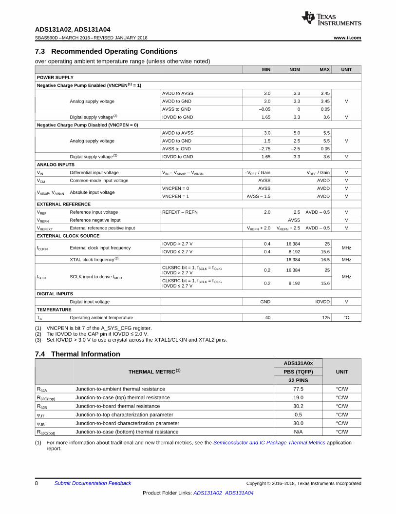
7.3 Recommended Operating Conditionsover operating ambient temperature range (unless otherwise noted)
MIN NOM MAX UNIT
POWER SUPPLY
Negative Charge Pump Enabled (VNCPEN (1) = 1)
Analog supply voltage
AVDD to AVSS 3.0 3.3 3.45
VAVDD to GND 3.0 3.3 3.45
AVSS to GND –0.05 0 0.05
Digital supply voltage (2) IOVDD to GND 1.65 3.3 3.6 V
Negative Charge Pump Disabled (VNCPEN = 0)
Analog supply voltage
AVDD to AVSS 3.0 5.0 5.5
VAVDD to GND 1.5 2.5 5.5
AVSS to GND –2.75 –2.5 0.05
Digital supply voltage (2) IOVDD to GND 1.65 3.3 3.6 V
ANALOG INPUTS
VIN Differential input voltage VIN = VAINxP – VAINxN –VREF / Gain VREF / Gain V
VCM Common-mode input voltage AVSS AVDD V
VAINxP, VAINxN Absolute input voltageVNCPEN = 0 AVSS AVDD V
VNCPEN = 1 AVSS – 1.5 AVDD V
EXTERNAL REFERENCE
VREF Reference input voltage REFEXT – REFN 2.0 2.5 AVDD – 0.5 V
VREFN Reference negative input AVSS V
VREFEXT External reference positive input VREFN + 2.0 VREFN + 2.5 AVDD – 0.5 V
EXTERNAL CLOCK SOURCE
fCLKIN External clock input frequencyIOVDD > 2.7 V 0.4 16.384 25
MHzIOVDD ≤ 2.7 V 0.4 8.192 15.6
XTAL clock frequency (3) 16.384 16.5 MHz
fSCLK SCLK input to derive fMOD
CLKSRC bit = 1, fSCLK = fICLK,IOVDD > 2.7 V 0.2 16.384 25
MHzCLKSRC bit = 1, fSCLK = fICLK,IOVDD ≤ 2.7 V 0.2 8.192 15.6
DIGITAL INPUTS
Digital input voltage GND IOVDD V
TEMPERATURE
TA Operating ambient temperature –40 125 °C
(1) For more information about traditional and new thermal metrics, see the Semiconductor and IC Package Thermal Metrics applicationreport.
7.4 Thermal Information
THERMAL METRIC (1)ADS131A0x
UNITPBS (TQFP)32 PINS
RθJA Junction-to-ambient thermal resistance 77.5 °C/WRθJC(top) Junction-to-case (top) thermal resistance 19.0 °C/WRθJB Junction-to-board thermal resistance 30.2 °C/WψJT Junction-to-top characterization parameter 0.5 °C/WψJB Junction-to-board characterization parameter 30.0 °C/WRθJC(bot) Junction-to-case (bottom) thermal resistance N/A °C/W

9
ADS131A02, ADS131A04www.ti.com SBAS590D –MARCH 2016–REVISED JANUARY 2018
Product Folder Links: ADS131A02 ADS131A04
Submit Documentation FeedbackCopyright © 2016–2018, Texas Instruments Incorporated
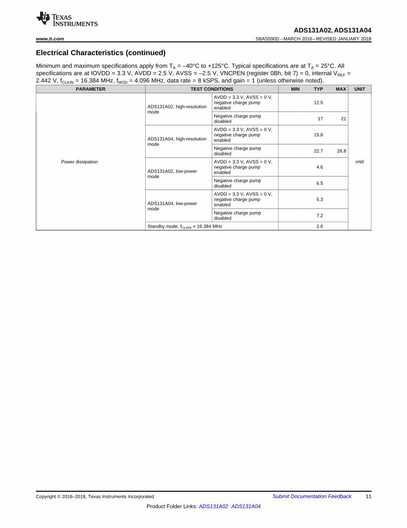
7.5 Electrical CharacteristicsMinimum and maximum specifications apply from TA = –40°C to +125°C. Typical specifications are at TA = 25°C. Allspecifications are at IOVDD = 3.3 V, AVDD = 2.5 V, AVSS = –2.5 V, VNCPEN (register 0Bh, bit 7) = 0, internal VREF =2.442 V, fCLKIN = 16.384 MHz, fMOD = 4.096 MHz, data rate = 8 kSPS, and gain = 1 (unless otherwise noted).
PARAMETER TEST CONDITIONS MIN TYP MAX UNIT
ANALOG INPUTS
Cs Input capacitance 3.5 pF
Zin Differential input impedance fMOD = 4.096 MHz 130 kΩ
ADC PERFORMANCE
Resolution 24 Bits
Gain 1, 2, 4, 8, 16
Data rate fMOD = 4.096 MHz 1 128 kSPS
DC PERFORMANCE
Dynamic range
105 111dB
AVDD – AVSS = 5 V, VREF = 4 V, VNCPEN bit = 0 115
All other settings See Noise Measurementssection
INL Integral nonlinearity Best fit 8 20 ppm
Offset error 500 µV
Offset drift 2.5 4 µV/°C
Gain error Excluding voltage reference and reference buffer error ±0.03 % of FS
Gain drift Excluding voltage reference and reference buffer error 0.5 2 ppm/°C
AC PERFORMANCE
CMRR Common-mode rejection ratio fCM = 50 Hz or 60 Hz 100 dB
PSRR Power-supply rejection ratioAVDD supply, fPS = 50 Hz and 60 Hz 80
dBIOVDD supply, fPS = 50 Hz and 60 Hz 105
Crosstalk fIN = 50 Hz and 60 Hz –125 dB
SNR Signal-to-noise ratio
fIN = 50 Hz or 60 Hz, VREF = 2.442 V, VIN = –20 dBFS,normalized 111
dBfIN = 50 Hz or 60 Hz, VREF = 4.0 V, VIN = –20 dBFS,normalized 115
THD Total harmonic distortion
fIN = 50 Hz or 60 Hz (up to 50 harmonics), VIN = –0.5 dBFS,ADS131A02 –101.5
dBfIN = 50 Hz or 60 Hz (up to 50 harmonics), VIN = –0.5 dBFS,ADS131A04 –103.5
SINAD Signal-to-noise + distortion fIN = 50 Hz or 60 Hz (up to 50 harmonics), VIN = –0.5 dBFS 101 dB
SFDR Spurious-free dynamic range
fIN = 50 Hz or 60 Hz (up to 50 harmonics), VIN = –0.5 dBFS,ADS131A02 102.5
dBfIN = 50 Hz or 60 Hz (up to 50 harmonics), VIN = –0.5 dBFS,ADS131A04 105
EXTERNAL REFERENCE
Reference buffer offset TA = 25°C 250 µV
Reference buffer offset drift –40°C ≤ TA ≤ +125°C 4 7 µV/°C
REFEXT input impedance 50 MΩ

10
ADS131A02, ADS131A04SBAS590D –MARCH 2016–REVISED JANUARY 2018 www.ti.com
Product Folder Links: ADS131A02 ADS131A04
Submit Documentation Feedback Copyright © 2016–2018, Texas Instruments Incorporated
Electrical Characteristics (continued)Minimum and maximum specifications apply from TA = –40°C to +125°C. Typical specifications are at TA = 25°C. Allspecifications are at IOVDD = 3.3 V, AVDD = 2.5 V, AVSS = –2.5 V, VNCPEN (register 0Bh, bit 7) = 0, internal VREF =2.442 V, fCLKIN = 16.384 MHz, fMOD = 4.096 MHz, data rate = 8 kSPS, and gain = 1 (unless otherwise noted).
PARAMETER TEST CONDITIONS MIN TYP MAX UNIT
INTERNAL REFERENCE VOLTAGE (REFP – REFN)
VREF Reference output voltageVREF_4V bit = 0 2.442
VVREF_4V bit = 1, AVDD – AVSS > 4.5 V 4.0
Accuracy ±0.1%
Temperature drift Including reference buffer drift, –40°C ≤ TA ≤ +125°C 6 20 ppm/°C
Start-up time
REFEXT = 1-µF to AVSS, settled to 1% 0.2
msREFEXT = 1-µF to AVSS, settled to 0.1% 1.2
REFEXT = 1-µF to AVSS, settled to 0.01% 250
REFP source capability 100 µA
EXTERNAL CLOCK SOURCE
fICLKInternal ICLK frequency (SCLK outputin master mode) CLKSRC bit = 0 0.2 8.192 12.5 MHz
fMOD ADC modulator frequency
High-resolution modeVNCPEN bit = 0 0.1 4.096 4.25
MHzVNCPEN bit = 1 0.512 4.096 4.25
Low-power modeVNCPEN bit = 0 0.1 1.024 1.05
VNCPEN bit = 1 0.512 1.024 1.05
DIGITAL INPUT/OUTPUT
VIH High-level input voltage 0.8 IOVDD IOVDD V
VIL Low-level input voltage GND 0.2 IOVDD V
VOH High-level output voltage IOH = 1 mA 0.8 IOVDD V
VOL Low-level output voltage IOL = –1 mA 0.2 IOVDD V
IIN Input current 0 V < VDigital Input < IOVDD –10 10 μA
POWER-SUPPLY
VNCP Negative charge pump output voltage –2 –1.65 V
AVDD current
ADS131A02, high-resolutionmode
AVDD = 3.3 V, AVSS = 0 V,negative charge pumpenabled
3.2
mA
Negative charge pumpdisabled 3 3.75
ADS131A04, high-resolutionmode
AVDD = 3.3 V, AVSS = 0 V,negative charge pumpenabled
4
Negative charge pumpdisabled 4 4.7
ADS131A02, low-power mode 0.9
ADS131A04, low-power mode 1.1
IOVDD current
ADS131A02, high-resolutionmode
AVDD = 3.3 V, AVSS = 0 V,negative charge pumpenabled
0.6
mA
Negative charge pumpdisabled 0.6 0.8
ADS131A04, high-resolutionmode
AVDD = 3.3 V, AVSS = 0 V,negative charge pumpenabled
0.8
Negative charge pumpdisabled 0.8 1.0
ADS131A02, low-power mode 0.5
ADS131A04, low-power mode 0.5
11
ADS131A02, ADS131A04www.ti.com SBAS590D –MARCH 2016–REVISED JANUARY 2018
Product Folder Links: ADS131A02 ADS131A04
Submit Documentation FeedbackCopyright © 2016–2018, Texas Instruments Incorporated
Electrical Characteristics (continued)Minimum and maximum specifications apply from TA = –40°C to +125°C. Typical specifications are at TA = 25°C. Allspecifications are at IOVDD = 3.3 V, AVDD = 2.5 V, AVSS = –2.5 V, VNCPEN (register 0Bh, bit 7) = 0, internal VREF =2.442 V, fCLKIN = 16.384 MHz, fMOD = 4.096 MHz, data rate = 8 kSPS, and gain = 1 (unless otherwise noted).
PARAMETER TEST CONDITIONS MIN TYP MAX UNIT
Power dissipation
ADS131A02, high-resolutionmode
AVDD = 3.3 V, AVSS = 0 V,negative charge pumpenabled
12.5
mW
Negative charge pumpdisabled 17 21
ADS131A04, high-resolutionmode
AVDD = 3.3 V, AVSS = 0 V,negative charge pumpenabled
15.8
Negative charge pumpdisabled 22.7 26.8
ADS131A02, low-powermode
AVDD = 3.3 V, AVSS = 0 V,negative charge pumpenabled
4.6
Negative charge pumpdisabled 6.5
ADS131A04, low-powermode
AVDD = 3.3 V, AVSS = 0 V,negative charge pumpenabled
5.3
Negative charge pumpdisabled 7.2
Standby mode, fCLKIN = 16.384 MHz 2.6
12
ADS131A02, ADS131A04SBAS590D –MARCH 2016–REVISED JANUARY 2018 www.ti.com
Product Folder Links: ADS131A02 ADS131A04
Submit Documentation Feedback Copyright © 2016–2018, Texas Instruments Incorporated
7.6 Timing Requirements: Asynchronous Interrupt Interface Modeover operating ambient temperature range (unless otherwise noted)
1.65 V ≤ IOVDD ≤ 2.7 V 2.7 V < IOVDD ≤ 3.6 VUNITMIN MAX MIN MAX
tc(CLKIN) External clock periodSingle device 64 40
nsMultiple device chaining 88 56
tw(CP)Pulse duration,CLKIN high or low
Single device 32 20ns
Multiple device chaining 44 28td(CSSC) Delay time, CS falling edge to first SCLK rising edge 16 16 nstd(SCS) Delay time, SCLK falling edge to CS falling edge 5 4 ns
tc(SC) SCLK periodSingle device 64 40
nsMultiple device chaining 88 64
tw(SCHL)Pulse duration,SCLK high or low
Single device 32 20ns
Multiple device chaining 44 32td(SCCS) Delay time, final SCLK falling edge to CS rising edge 5 5 nstsu(DI) Setup time, DIN valid before SCLK falling edge 5 5 nsth(DI) Hold time, DIN valid after SCLK falling edge 8 8 nstw(CSH) Pulse duration, CS high 20 15 nstw(RSL) Pulse duration, RESET low 800 800 ns
7.7 Switching Characteristics: Asynchronous Interrupt Interface Modeover operating ambient temperature range (unless otherwise noted)
1.65 V ≤ IOVDD ≤ 2.7 V 2.7 V < IOVDD ≤ 3.6 VUNITMIN MAX MIN MAX
tp(SCDOD)Propagation delay time,first SCLK rising edge to DOUT driven 28 15 ns
tp(SCDO)Propagation delay time,SCLK rising edge to valid new DOUT 26 15 ns
th(LSB)Hold time, last SCLK falling edgeto DOUT 3-state
HIZDLY = 00 6 30 6 20
nsHIZDLY = 01 8 37 8 27HIZDLY = 10 10 43 10 43HIZDLY = 11 12 47 12 47
tp(DN)Propagation delay time, SCLKfalling edge to DONE falling edge
DNDLY = 00 6 33 6 21
nsDNDLY = 01 8 39 8 27DNDLY = 10 10 44 10 32DNDLY = 11 12 48 12 36
tp(CSDN)Propagation delay time,CS rising edge to DONE rising edge 32 32 ns
tp(CSDR)Propagation delay time,CS rising edge to DRDY rising edge 2.0 2.0 tICLK
td(RSSC)Delay time,RESET rising edge to READY response 4.5 4.5 ms

13
ADS131A02, ADS131A04www.ti.com SBAS590D –MARCH 2016–REVISED JANUARY 2018
Product Folder Links: ADS131A02 ADS131A04
Submit Documentation FeedbackCopyright © 2016–2018, Texas Instruments Incorporated
7.8 Timing Requirements: Synchronous Master Interface Modeover operating ambient temperature range (unless otherwise noted)
1.65 V ≤ IOVDD ≤ 2.7 V 2.7 V < IOVDD ≤ 3.6 VUNITMIN MAX MIN MAX
tc(CLKIN) External clock periodSingle device 64 40
nsMultiple device chaining 88 56
tw(CP)Pulse duration,CLKIN high or low
Single device 32 20ns
Multiple device chaining 44 28tc(SC) SCLK period 2 2 tCLKIN
tw(SCHL) Pulse duration, SCLK high or low 1 1 tCLKIN
tsu(DI) Setup time, DIN valid before SCLK falling edge 5 5 nsth(DI) Hold time, DIN valid after SCLK falling edge 8 8 nstw(RSL) Pulse duration, RESET low 800 800 ns
7.9 Switching Characteristics: Synchronous Master Interface Modeover operating ambient temperature range (unless otherwise noted)
1.65 V ≤ IOVDD ≤ 2.7 V 2.7 V < IOVDD ≤ 3.6 VUNITMIN MAX MIN MAX
tp(SCDOD)Propagation delay time,first SCLK rising edge to DOUT driven 28 15 ns
tp(SCDO)Propagation delay time,SCLK rising edge to valid new DOUT 26 15 ns
tp(SDR)Propagation delay time,SCLK falling edge to DRDY falling edge 31 20 ns
th(LSB)Hold time, last SCLK falling edgeto DOUT 3-state
HIZDLY = 00 6 30 6 20
nsHIZDLY = 01 8 37 8 27HIZDLY = 10 10 43 10 43HIZDLY = 11 12 47 12 47
tp(DN)Propagation delay time, SCLKfalling edge to DONE falling edge
DNDLY = 00 6 33 6 21
nsDNDLY = 01 8 39 8 27DNDLY = 10 10 44 10 32DNDLY = 11 12 48 12 36
tp(CSDN)Propagation delay time,CS rising edge to DONE rising edge 32 32 ns
tp(DRS)Delay time,last SCLK rising edge to DRDY rising edge 17 15 ns
td(RSSC)Delay time,RESET rising edge to READY response 4.5 4.5 ms

14
ADS131A02, ADS131A04SBAS590D –MARCH 2016–REVISED JANUARY 2018 www.ti.com
Product Folder Links: ADS131A02 ADS131A04
Submit Documentation Feedback Copyright © 2016–2018, Texas Instruments Incorporated
(1) Only valid if CLKSRC = 0
7.10 Timing Requirements: Synchronous Slave Interface Modeover operating ambient temperature range (unless otherwise noted)
1.65 V ≤ IOVDD ≤ 2.7 V 2.7 V < IOVDD ≤ 3.6 VUNITMIN MAX MIN MAX
tc(CLKIN) External clock period (1) Single device 64 40ns
Multiple device chaining 88 56
tw(CP)Pulse duration,CLKIN high or low (1)
Single device 32 20ns
Multiple device chaining 44 28td(SCS) Delay time, SCLK falling edge to CS falling edge 6 4 nstd(CSSC) Delay time, CS falling edge to first SCLK rising edge 16 16 ns
tc(SC) SCLK periodSingle device 64 40
nsMultiple device chaining 88 64
tw(SCHL)Pulse duration,SCLK high or low
Single device 32 20ns
Multiple device chaining 44 32tsu(DI) Setup time, DIN valid before SCLK falling edge 5 5 nsth(DI) Hold time, DIN valid after SCLK falling edge 8 6 nstd(SCCS) Delay time, last SCLK falling edge to CS rising edge 5 5 ns
tsu(sync)Setup time, DRDY falling edge to master clock fallingedge 10 10 ns
th(sync) Hold time, DRDY low after master clock falling edge 10 10 nstDATA Data rate period Set by the CLK1 register and the CLK2 registertw(RSL) Pulse duration RESET low 800 800 ns
7.11 Switching Characteristics: Synchronous Slave Interface Modeover operating ambient temperature range (unless otherwise noted)
1.65 V ≤ IOVDD ≤ 2.7 V 2.7 V < IOVDD ≤ 3.6 VUNITMIN MAX MIN MAX
tp(SCDOD)Propagation delay time,first SCLK rising edge to DOUT driven 28 15 ns
tp(SCDO)Propagation delay time,SCLK rising edge to valid new DOUT 26 15 ns
th(LSB)Hold time, last SCLK falling edgeto DOUT 3-state
HIZDLY = 00 6 30 6 20
nsHIZDLY = 01 8 37 8 27HIZDLY = 10 10 43 10 43HIZDLY = 11 12 47 12 47
tp(DN)Propagation delay time, SCLKfalling edge to DONE falling edge
DNDLY = 00 6 33 6 21
nsDNDLY = 01 8 39 8 27DNDLY = 10 10 44 10 32DNDLY = 11 12 48 12 36
tp(CSDN)Propagation delay time,CS rising edge to DONE rising edge 32 32 ns
td(RSSC)Delay time,RESET rising edge to READY response 4.5 4.5 ms

CS
SCLK
DIN
td(SCS)
tp(SCDO)
tw(SCHL)
DOUT
tsu(DI) th(DI)
§
§
§§
MSB MSB - 1 LSB + 1 LSB
§§
tp(SCCS)tc(SC)
CLKINtc(CLKIN)
tw(CP)
§
§
§
§
th(LSB)
§
tp(SCDOD)
td(CSSC)
DRDY
SCLK
DIN
tp(SDR)
tp(SCDO)
tw(SCHL)
DOUT
tsu(DI) th(DI)
§
§
§§
MSB MSB - 1 LSB + 1 LSB
§§
tp(DRS)tc(SC)
CLKINtc(CLKIN)
tw(CP)
§
§
§
§
th(LSB)
§
tp(SCDOD)
CS
SCLK
DIN
td(CSSC)
tp(SCDO)
tw(SCHL)
tsu(DI) th(DI)
§
§
§§
td(SCCS)
DRDY §
tp(CSDR)
tc(SC)
CLKINtc(CLKIN)
tw(CP)
DOUT MSB MSB - 1 LSB + 1 LSB
§§
th(LSB)
td(SCS)
tp(SCDOD)
tw(CSH)
15
ADS131A02, ADS131A04www.ti.com SBAS590D –MARCH 2016–REVISED JANUARY 2018
Product Folder Links: ADS131A02 ADS131A04
Submit Documentation FeedbackCopyright © 2016–2018, Texas Instruments Incorporated
NOTE: SPI settings are CPOL = 0 and CPHA = 1. CS transitions must take place when SCLK is low.
Figure 1. Asynchronous Interrupt Mode SPI Timing Diagram
NOTE: SPI settings are CPOL = 0 and CPHA = 1.
Figure 2. Synchronous Master Mode SPI Timing Diagram
NOTE: SPI settings are CPOL = 0 and CPHA = 1. CS can be tied directly to DRDY.
Figure 3. Synchronous Slave Mode SPI Timing Diagram

DIN
DOUT
tw(RSL)RESET §
§
§
§
td(RSSC)
or
RESET
§
Ready
§
§
CS
SCLK
DIN, DOUT
tp(DN)
LSB + 1 LSB
DONE
tp(CSDN)
DRDY
SCLK
Optional Pulse
tsu(sync)
th(sync)
tDATA
Optional Pulse
tDATA
DRDY
CLKIN
Optional Pulse
tsu(sync)
th(sync)
tDATA
Optional Pulse
tDATA
16
ADS131A02, ADS131A04SBAS590D –MARCH 2016–REVISED JANUARY 2018 www.ti.com
Product Folder Links: ADS131A02 ADS131A04
Submit Documentation Feedback Copyright © 2016–2018, Texas Instruments Incorporated
Figure 4. DRDY Synchronization Timing for Synchronous Slave Mode (CLKSRC = 0)
Figure 5. DRDY Synchronization Timing for Synchronous Slave Mode (CLKSRC = 1)
Figure 6. DONE Signal Timing
Figure 7. RESET Pin and Command Timing

Frequency (Hz)
Am
plitu
de (
dB)
0 500 1000 1500 2000 2500 3000 3500 4000-180
-160
-140
-120
-100
-80
-60
-40
-20
0
D011Frequency (Hz)
Am
plitu
de (
dB)
0 500 1000 1500 2000 2500 3000 3500 4000-180
-160
-140
-120
-100
-80
-60
-40
-20
0
D012
Input Referred Voltage (PV)
Num
ber
of O
ccur
renc
es
0
5000
10000
15000
20000
25000
30000
-20 -15 -10 -5 0 5 10 15 20
D001 Effective Number of Bits
Num
ber
of O
ccur
renc
es
05
1015202530354045505560657075
18 18.1 18.2 18.3 18.4
D001
Time (s)
Inpu
t-R
efer
red
Noi
se (P
V)
0 1 2 3 4 5 6 7 8-25
-20
-15
-10
-5
0
5
10
15
20
25
D008Input Referred Voltage (PV)
Num
ber
of O
ccur
renc
es
0
2000
4000
6000
8000
10000
12000
14000
16000
-10 -5 0 5 10
D001
17
ADS131A02, ADS131A04www.ti.com SBAS590D –MARCH 2016–REVISED JANUARY 2018
Product Folder Links: ADS131A02 ADS131A04
Submit Documentation FeedbackCopyright © 2016–2018, Texas Instruments Incorporated
7.12 Typical Characteristicsat TA = 25°C, IOVDD = 3.3 V, AVDD = 2.5 V, AVSS = –2.5 V, VNCPEN (register 0Bh, bit 7) = 0, internal VREF = 2.442 V,fCLKIN = 16.384 MHz, fMOD = 4.096 MHz, data rate = 8 kSPS, HR mode, and gain = 1 (unless otherwise noted)
Shorted inputs, 65536 points
Figure 8. Input-Referred Noise vs Time
Shorted inputs, 1 kSPS, 65536 points, offset removed
Figure 9. Single Device Noise Histogram
Shorted inputs, 8 kSPS, 262144 points, offset removed
Figure 10. Single Device Noise Histogram
Shorted inputs, 8 kSPS, 560 devices, multiple lots
Figure 11. Multiple Device Effective Resolution Histogram
fIN = 60 Hz, 32768 points
Figure 12. THD FFT Plot at 8 kSPS and –0.5 dBFS
fIN = 60 Hz, 32768 points
Figure 13. THD FFT Plot at 8 kSPS and –20 dBFS

Input Voltage (V)
Inte
gral
Non
linea
rity
(ppm
)
-2.5 -2 -1.5 -1 -0.5 0 0.5 1 1.5 2 2.5-7
-6
-5
-4
-3
-2
-1
0
1
2
3
4
D001
Ta = -40Ta = 25Ta = 125
Temperature (qC)
Noi
se (P
Vrm
s)
-50 -25 0 25 50 75 100 1254.4
4.6
4.8
5
5.2
5.4
D018
Ch 1Ch 2Ch 3Ch 4
Frequency (Hz)
Am
plitu
de (
dB)
0 1000 2000 3000 4000 5000 6000 7000 8000-180
-160
-140
-120
-100
-80
-60
-40
-20
0
D028Input Frequency (Hz)
TH
D (
dB)
0 500 1000 1500 2000 2500 3000 3500 4000-150
-145
-140
-135
-130
-125
-120
-115
-110
-105
-100
-95
-90
D001
Frequency (Hz)
Am
plitu
de (
dB)
0 1000 2000 3000 4000 5000 6000 7000 8000-180
-160
-140
-120
-100
-80
-60
-40
-20
0
D029Frequency (Hz)
Am
plitu
de (
dB
0 5 10 15 20 25 30 35 40 45 50 55 60 65 70-180
-160
-140
-120
-100
-80
-60
-40
-20
0
D001
18
ADS131A02, ADS131A04SBAS590D –MARCH 2016–REVISED JANUARY 2018 www.ti.com
Product Folder Links: ADS131A02 ADS131A04
Submit Documentation Feedback Copyright © 2016–2018, Texas Instruments Incorporated
Typical Characteristics (continued)at TA = 25°C, IOVDD = 3.3 V, AVDD = 2.5 V, AVSS = –2.5 V, VNCPEN (register 0Bh, bit 7) = 0, internal VREF = 2.442 V,fCLKIN = 16.384 MHz, fMOD = 4.096 MHz, data rate = 8 kSPS, HR mode, and gain = 1 (unless otherwise noted)
fIN = 60 Hz, 8 kSPS
Figure 14. Low-Frequency FFT Plot
fIN = 60 Hz, 32768 points
Figure 15. THD FFT Plot at 16 kSPS and –0.5 dBFS
fIN = 60 Hz, 32768 points
Figure 16. THD FFT Plot at 16 kSPS and –20 dBFS Figure 17. THD vs Input Frequency
Figure 18. INL vs Temperature Figure 19. Noise RMS vs Temperature

Input Voltage (dBFS)
Nor
mal
ized
TH
D (
dB)
-35 -30 -25 -20 -15 -10 -5 0-135
-130
-125
-120
-115
-110
-105
-100
D001
Ta = -40qCTa = 25qCTa = 125qC
Frequency (Hz)
CM
RR
(dB
)
0 2000 4000 6000 800090
100
110
120
130
140
D009
Ta = -40 qCTa = 25 qCTa = 125 qC
Temperature (qC)
Ref
eren
ce V
otla
ge (
V)
-50 -25 0 25 50 75 100 1252.44
2.442
2.444
2.446
2.448
D013Input Voltage (dBFS)
Nor
mal
ized
SN
R (
dB)
-120 -100 -80 -60 -40 -20 0107
107.5
108
108.5
109
109.5
110
110.5
111
111.5
112
D001
Ta = -40qCTa = 25qCTa = 125qC
Temperature (qC)
Offs
et E
rror
(P
V)
-50 -25 0 25 50 75 100 125400
500
600
700
800
900
D020
Ch 1Ch 2Ch 3Ch 4
Temperature (qC)
Gai
n E
rror
(%
of F
S)
-50 -25 0 25 50 75 100 125-0.05
-0.025
0
0.025
0.05
D021
Ch 1Ch 2Ch 3Ch 4
19
ADS131A02, ADS131A04www.ti.com SBAS590D –MARCH 2016–REVISED JANUARY 2018
Product Folder Links: ADS131A02 ADS131A04
Submit Documentation FeedbackCopyright © 2016–2018, Texas Instruments Incorporated
Typical Characteristics (continued)at TA = 25°C, IOVDD = 3.3 V, AVDD = 2.5 V, AVSS = –2.5 V, VNCPEN (register 0Bh, bit 7) = 0, internal VREF = 2.442 V,fCLKIN = 16.384 MHz, fMOD = 4.096 MHz, data rate = 8 kSPS, HR mode, and gain = 1 (unless otherwise noted)
Figure 20. Offset Error vs Temperature Figure 21. Gain Error vs Temperature
30 units, multiple lots
Figure 22. Internal VREF vs Temperature Figure 23. Normalized SNR vs Amplitude
Figure 24. Normalized THD vs Amplitude Figure 25. CMRR vs Frequency

Temperature (qC)
Diff
eren
tial I
nput
Impe
danc
e (k:
)
-40 -20 0 20 40 60 80 100 120559
559.5
560
560.5
561
561.5
562
562.5
563
563.5
564
564.5
D001fMOD (MHz)
AV
DD
Cur
rent
(P
A)
0 0.5 1 1.5 2 2.5 3 3.5 4 4.5 50
500
1000
1500
2000
2500
3000
3500
4000
4500
D001
ADS131A04 LPMADS131A04 HRM
fMOD (Hz)
Diff
eren
tial I
nput
Impe
danc
e (k:
)
0 1000000 2000000 3000000 40000000
5001000150020002500300035004000450050005500600065007000
D001Temperature (qC)
Diff
eren
tial I
nput
Impe
danc
e (k:
)
-40 -20 0 20 40 60 80 100 120140
140.1
140.2
140.3
140.4
140.5
140.6
140.7
140.8
140.9
141
141.1
141.2
141.3
D001
Frequency (Hz)
AC
PS
RR
(dB
)
10 20 100 1000 10000 100000 1000000 1E+70
20
40
60
80
100
120
D019
AVDDIOVDD
Crosstalk (dB)
Num
ber
of O
ccur
renc
es
0
5
10
15
20
25
30
35
40
-135 -130 -125 -120
D001
Channel 1Channel 2Channel 3Channel 4
20
ADS131A02, ADS131A04SBAS590D –MARCH 2016–REVISED JANUARY 2018 www.ti.com
Product Folder Links: ADS131A02 ADS131A04
Submit Documentation Feedback Copyright © 2016–2018, Texas Instruments Incorporated
Typical Characteristics (continued)at TA = 25°C, IOVDD = 3.3 V, AVDD = 2.5 V, AVSS = –2.5 V, VNCPEN (register 0Bh, bit 7) = 0, internal VREF = 2.442 V,fCLKIN = 16.384 MHz, fMOD = 4.096 MHz, data rate = 8 kSPS, HR mode, and gain = 1 (unless otherwise noted)
Figure 26. PSRR vs Frequency Figure 27. Crosstalk Histogram
Figure 28. Differential Input Impedance vsModulator Clock
Figure 29. Differential Input Impedance vsTemperature at 4.096-MHz fMOD
Figure 30. Differential Input Impedance vsTemperature at 1.024-MHz fMOD
LPM = low-power mode, HRM = high-resolution mode
Figure 31. ADS131A04 AVDD Current vs fMOD

fMOD (MHz)
IOV
DD
Cur
rent
(P
A)
0 0.5 1 1.5 2 2.5 3 3.5 4 4.5 550
100150200250300350400450500550600650700750800
D001
ADS131A02 HRMADS131A02 LPM
fMOD (MHz)
IOV
DD
Cur
rent
(P
A)
0 0.5 1 1.5 2 2.5 3 3.5 4 4.50
100
200
300
400
500
600
700
800
900
D001
ADS131A04 LPMADS131A04 HRM
fMOD (MHz)
AV
DD
Cur
rent
(P
A)
0 0.5 1 1.5 2 2.5 3 3.5 4 4.5 5300
600
900
1200
1500
1800
2100
2400
2700
3000
3300
3600
D001
ADS131A02 HRMADS131A02 LPM
21
ADS131A02, ADS131A04www.ti.com SBAS590D –MARCH 2016–REVISED JANUARY 2018
Product Folder Links: ADS131A02 ADS131A04
Submit Documentation FeedbackCopyright © 2016–2018, Texas Instruments Incorporated
Typical Characteristics (continued)at TA = 25°C, IOVDD = 3.3 V, AVDD = 2.5 V, AVSS = –2.5 V, VNCPEN (register 0Bh, bit 7) = 0, internal VREF = 2.442 V,fCLKIN = 16.384 MHz, fMOD = 4.096 MHz, data rate = 8 kSPS, HR mode, and gain = 1 (unless otherwise noted)
LPM = low-power mode, HRM = high-resolution mode
Figure 32. ADS131A04 IOVDD Current vs fMOD
LPM = low-power mode, HRM = high-resolution mode
Figure 33. ADS131A02 AVDD Current vs fMOD
LPM = low-power mode, HRM = high-resolution mode
Figure 34. ADS131A02 IOVDD Current vs fMOD
REF
RMS
VDynamic Range = 20 log
2 Gain V
§ ·u ¨ ¸¨ ¸u u© ¹
REF2
RMS
2 VEffective Resolution = log
Gain V
§ ·u¨ ¸
u© ¹
22
ADS131A02, ADS131A04SBAS590D –MARCH 2016–REVISED JANUARY 2018 www.ti.com
Product Folder Links: ADS131A02 ADS131A04
Submit Documentation Feedback Copyright © 2016–2018, Texas Instruments Incorporated
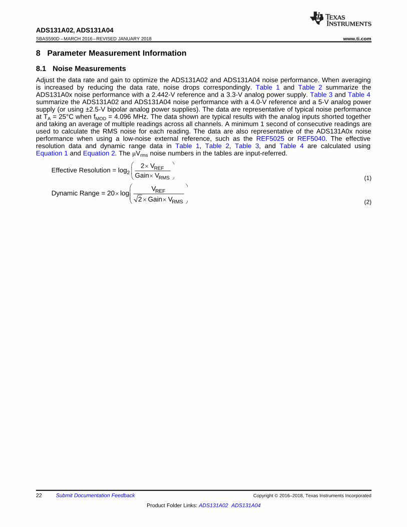
8 Parameter Measurement Information
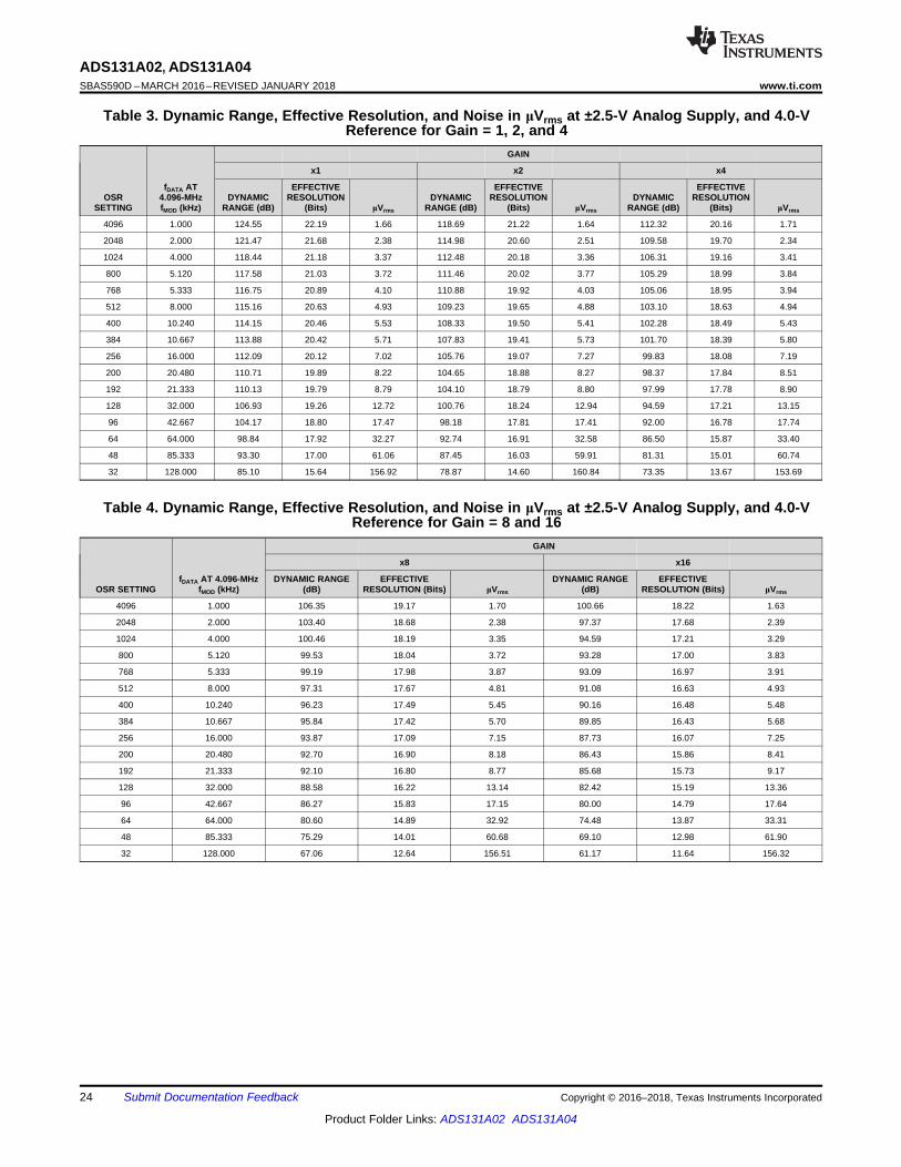
8.1 Noise MeasurementsAdjust the data rate and gain to optimize the ADS131A02 and ADS131A04 noise performance. When averagingis increased by reducing the data rate, noise drops correspondingly. Table 1 and Table 2 summarize theADS131A0x noise performance with a 2.442-V reference and a 3.3-V analog power supply. Table 3 and Table 4summarize the ADS131A02 and ADS131A04 noise performance with a 4.0-V reference and a 5-V analog powersupply (or using ±2.5-V bipolar analog power supplies). The data are representative of typical noise performanceat TA = 25°C when fMOD = 4.096 MHz. The data shown are typical results with the analog inputs shorted togetherand taking an average of multiple readings across all channels. A minimum 1 second of consecutive readings areused to calculate the RMS noise for each reading. The data are also representative of the ADS131A0x noiseperformance when using a low-noise external reference, such as the REF5025 or REF5040. The effectiveresolution data and dynamic range data in Table 1, Table 2, Table 3, and Table 4 are calculated usingEquation 1 and Equation 2. The μVrms noise numbers in the tables are input-referred.
(1)
(2)

23
ADS131A02, ADS131A04www.ti.com SBAS590D –MARCH 2016–REVISED JANUARY 2018
Product Folder Links: ADS131A02 ADS131A04
Submit Documentation FeedbackCopyright © 2016–2018, Texas Instruments Incorporated
Noise Measurements (continued)Table 1. Dynamic Range, Effective Resolution, and Noise in μVrms at 3.3-V Analog Supply, and 2.442-V
Reference for Gain = 1, 2, and 4
OSRSETTING
fDATA AT4.096-MHzfMOD (kHz)
GAIN
x1 x2 x4
DYNAMICRANGE (dB)
EFFECTIVERESOLUTION
(Bits) μVrms
DYNAMICRANGE (dB)
EFFECTIVERESOLUTION
(Bits) μVrms
DYNAMICRANGE (dB)
EFFECTIVERESOLUTION
(Bits) μVrms
4096 1.000 119.49 21.35 1.82 113.49 20.35 1.82 108.08 19.46 1.70
2048 2.000 116.47 20.85 2.58 110.97 19.94 2.44 105.22 18.98 2.36
1024 4.000 113.85 20.41 3.49 107.91 19.43 3.47 101.77 18.41 3.52
800 5.120 112.93 20.26 3.88 106.72 19.23 3.98 101.05 18.29 3.82
768 5.333 112.90 20.25 3.90 106.69 19.22 3.99 100.76 18.24 3.95
512 8.000 110.73 19.89 5.01 104.83 18.91 4.95 98.75 17.91 4.97
400 10.240 109.74 19.73 5.61 103.69 18.72 5.64 97.76 17.74 5.58
384 10.667 109.53 19.70 5.75 103.65 18.72 5.66 97.58 17.71 5.69
256 16.000 107.74 19.40 7.07 101.67 18.39 7.11 95.72 17.40 7.06
200 20.480 106.48 19.19 8.17 100.55 18.20 8.09 94.54 17.21 8.08
192 21.333 106.28 19.16 8.36 100.17 18.14 8.45 94.11 17.13 8.49
128 32.000 104.05 18.78 10.81 97.98 17.78 10.88 92.00 16.78 10.82
96 42.667 101.90 18.43 13.85 95.95 17.44 13.74 89.90 16.43 13.79
64 64.000 97.63 17.72 22.64 91.61 16.72 22.64 85.52 15.71 22.83
48 85.333 92.58 16.88 40.50 86.62 15.89 40.22 80.59 14.89 40.26
32 128.000 85.12 15.62 96.82 78.96 14.62 97.12 73.02 13.61 97.51
Table 2. Dynamic Range, Effective Resolution, and Noise in μVrms at 3.3-V Analog Supply, and 2.442-VReference for Gain = 8 and 16
OSR SETTINGfDATA AT 4.096-MHz
fMOD (kHz)
GAIN
x8 x16
DYNAMIC RANGE(dB)
EFFECTIVERESOLUTION (Bits) μVrms
DYNAMIC RANGE(dB)
EFFECTIVERESOLUTION (Bits) μVrms
4096 1.000 101.72 18.40 1.77 95.45 17.36 1.82
2048 2.000 98.88 17.93 2.45 93.07 16.96 2.39
1024 4.000 95.97 17.44 3.43 89.82 16.42 3.48
800 5.120 95.03 17.29 3.82 88.66 16.23 3.98
768 5.333 94.63 17.22 4.00 88.41 16.19 4.09
512 8.000 92.75 16.91 4.96 87.00 15.95 4.81
400 10.240 91.84 16.76 5.51 85.62 15.72 5.64
384 10.667 91.52 16.70 5.72 85.50 15.70 5.72
256 16.000 89.57 16.38 7.16 83.58 15.38 7.14
200 20.480 88.44 16.19 8.16 82.45 15.20 8.12
192 21.333 88.26 16.16 8.32 82.12 15.14 8.44
128 32.000 86.02 15.79 10.77 79.80 14.76 11.02
96 42.667 83.91 15.44 13.74 77.72 14.41 14.00
64 64.000 79.52 14.71 22.78 73.45 13.70 22.92
48 85.333 74.60 13.89 40.14 68.47 12.87 40.66
32 128.000 66.93 12.62 97.05 60.97 11.61 97.61
24
ADS131A02, ADS131A04SBAS590D –MARCH 2016–REVISED JANUARY 2018 www.ti.com
Product Folder Links: ADS131A02 ADS131A04
Submit Documentation Feedback Copyright © 2016–2018, Texas Instruments Incorporated
Table 3. Dynamic Range, Effective Resolution, and Noise in μVrms at ±2.5-V Analog Supply, and 4.0-VReference for Gain = 1, 2, and 4
OSRSETTING
fDATA AT4.096-MHzfMOD (kHz)
GAIN
x1 x2 x4
DYNAMICRANGE (dB)
EFFECTIVERESOLUTION
(Bits) μVrms
DYNAMICRANGE (dB)
EFFECTIVERESOLUTION
(Bits) μVrms
DYNAMICRANGE (dB)
EFFECTIVERESOLUTION
(Bits) μVrms
4096 1.000 124.55 22.19 1.66 118.69 21.22 1.64 112.32 20.16 1.71
2048 2.000 121.47 21.68 2.38 114.98 20.60 2.51 109.58 19.70 2.34
1024 4.000 118.44 21.18 3.37 112.48 20.18 3.36 106.31 19.16 3.41
800 5.120 117.58 21.03 3.72 111.46 20.02 3.77 105.29 18.99 3.84
768 5.333 116.75 20.89 4.10 110.88 19.92 4.03 105.06 18.95 3.94
512 8.000 115.16 20.63 4.93 109.23 19.65 4.88 103.10 18.63 4.94
400 10.240 114.15 20.46 5.53 108.33 19.50 5.41 102.28 18.49 5.43
384 10.667 113.88 20.42 5.71 107.83 19.41 5.73 101.70 18.39 5.80
256 16.000 112.09 20.12 7.02 105.76 19.07 7.27 99.83 18.08 7.19
200 20.480 110.71 19.89 8.22 104.65 18.88 8.27 98.37 17.84 8.51
192 21.333 110.13 19.79 8.79 104.10 18.79 8.80 97.99 17.78 8.90
128 32.000 106.93 19.26 12.72 100.76 18.24 12.94 94.59 17.21 13.15
96 42.667 104.17 18.80 17.47 98.18 17.81 17.41 92.00 16.78 17.74
64 64.000 98.84 17.92 32.27 92.74 16.91 32.58 86.50 15.87 33.40
48 85.333 93.30 17.00 61.06 87.45 16.03 59.91 81.31 15.01 60.74
32 128.000 85.10 15.64 156.92 78.87 14.60 160.84 73.35 13.67 153.69
Table 4. Dynamic Range, Effective Resolution, and Noise in μVrms at ±2.5-V Analog Supply, and 4.0-VReference for Gain = 8 and 16
OSR SETTINGfDATA AT 4.096-MHz
fMOD (kHz)
GAIN
x8 x16
DYNAMIC RANGE(dB)
EFFECTIVERESOLUTION (Bits) μVrms
DYNAMIC RANGE(dB)
EFFECTIVERESOLUTION (Bits) μVrms
4096 1.000 106.35 19.17 1.70 100.66 18.22 1.63
2048 2.000 103.40 18.68 2.38 97.37 17.68 2.39
1024 4.000 100.46 18.19 3.35 94.59 17.21 3.29
800 5.120 99.53 18.04 3.72 93.28 17.00 3.83
768 5.333 99.19 17.98 3.87 93.09 16.97 3.91
512 8.000 97.31 17.67 4.81 91.08 16.63 4.93
400 10.240 96.23 17.49 5.45 90.16 16.48 5.48
384 10.667 95.84 17.42 5.70 89.85 16.43 5.68
256 16.000 93.87 17.09 7.15 87.73 16.07 7.25
200 20.480 92.70 16.90 8.18 86.43 15.86 8.41
192 21.333 92.10 16.80 8.77 85.68 15.73 9.17
128 32.000 88.58 16.22 13.14 82.42 15.19 13.36
96 42.667 86.27 15.83 17.15 80.00 14.79 17.64
64 64.000 80.60 14.89 32.92 74.48 13.87 33.31
48 85.333 75.29 14.01 60.68 69.10 12.98 61.90
32 128.000 67.06 12.64 156.51 61.17 11.64 156.32

SCLK
DOUT
DIN
Control and Serial Interface
GNDAVSS
DRDY
AVDD
VNCP
XTAL1/CLKIN
CS
Negative Charge Pump
Voltage Reference
AD
S13
1A04
Onl
y
Reference Mux
REFEXT IOVDD
CLK/XTALXTAL2
M[2:0]
RESET
DONE
'6 ADC
'6 ADC
'6 ADC
'6 ADC
AIN4N
AIN4P
AIN3N
AIN3P
AIN2N
AIN2P
AIN1N
AIN1P
REFNREFP
Out-of-Range Detect
Data Integrity
WatchdogTimer
25
ADS131A02, ADS131A04www.ti.com SBAS590D –MARCH 2016–REVISED JANUARY 2018
Product Folder Links: ADS131A02 ADS131A04
Submit Documentation FeedbackCopyright © 2016–2018, Texas Instruments Incorporated
9 Detailed Description
9.1 OverviewThe ADS131A02 and ADS131A04 are low-power, two- and four-channel, simultaneous-sampling, 24-bit, delta-sigma (ΔΣ), analog-to-digital converters (ADCs) with an integrated low-drift internal reference voltage. Data rateflexibility, wide dynamic range, and interface options make these devices good choices when designing forsmart-grid and other industrial power monitor, control, and protection applications. The ADC interface dataintegrity features provide for a very low rate of transmission errors. Throughout this document, the ADS131A02and ADS131A04 are referred to as the ADS131A0x.
The ADS131A0x has very flexible power-supply options. A 5-V single-supply (or ±2.5-V bipolar-supply) operationis available to support up to a 4.5-V external reference to maximize the dynamic range of the converter.Alternatively, a negative charge pump can be enabled to accept absolute input signals down to –1.5 V belowground when powered from a single 3.3-V supply. Five gain options are available to help maximize the ADCcode range and 16 selectable oversampling ratio (OSR) options are selectable to optimize the converter for aspecific data rate. The low-drift internal reference can be programmed to either 2.442 V or 4 V. Input signal out-of-range detection can be accomplished by using the integrated comparators, with programmable trigger-pointsettings. A detailed diagram of the ADS131A0x is shown in the Functional Block Diagram section.
The device offers multiple serial peripheral interface (SPI) communication options to provide flexibility forinterfacing to microprocessors or field-programmable gate arrays (FPGAs). Synchronous real-time andasynchronous interrupt communication modes are available using the SPI-compatible interface. Multiple devicescan share a common SPI port and are synchronized by using the DRDY signal. Device communication isspecified through configuration of the M0 interface mode pin and chaining of the DONE signal. Optional cyclicredundancy check (CRC) and hamming code correction on the interface enhance communication integrity.
9.2 Functional Block Diagram

Sinc3 LPF
SPI+
Ctrl
CS
DONE
DIN
XTAL1/CLKIN
XTAL2X
MCLK_DIV
[2:0]ICLK_DIV
[2:0]OSR [3:0]
AINxP
AINxN
DRDY
M0
sync
ADC
fICLK
fMOD
fDATA
fCLKINCLKSRC DOUT
SCLK
26
ADS131A02, ADS131A04SBAS590D –MARCH 2016–REVISED JANUARY 2018 www.ti.com
Product Folder Links: ADS131A02 ADS131A04
Submit Documentation Feedback Copyright © 2016–2018, Texas Instruments Incorporated
9.3 Feature DescriptionThis section contains details of the ADS131A0x internal feature elements. The ADC clocking is discussed first,followed by the analog blocks and the digital filter.
9.3.1 ClockMultiple clocks are created from one external master clock source in the ADS131A0x to create deviceconfiguration flexibility. The ADC operates from the internal system clock, ICLK, which is provided in one of threeways.• An external master clock, CLKIN, can be applied directly to the XTAL1/CLKIN pin to be divided down to
generate ICLK using the CLK_DIV[2:0] bits in the CLK1 register. In this case, leave the XTAL2 pin floating.• A crystal oscillator can be applied between XTAL1/CLKIN and XTAL2, generating a master clock to be
divided down using the CLK_DIV[2:0] bits in the CLK1 register to generate ICLK.• A free-running SCLK can be internally routed to be set as ICLK. This mode is only available in synchronous
slave interface mode. Tie the CLKIN/XTAL1 pin to GND. Leave the XTAL2 pin unconnected.
The system ICLK is passed through a second 3-bit clock divider (ICLK_DIV[2:0] in the CLK2 register) to createthe modulator clock, MODCLK. MODCLK is used for timing of the delta-sigma (ΔΣ) modulator sampling anddigital filter.
The interface operation mode determines the options for sourcing ICLK. When in asynchronous interrupt orsynchronous master mode, generate ICLK by applying a direct external master clock signal to the XTAL1/CLKINpin or by using a crystal oscillator across the XTAL1/CLKIN and XTAL2 pins. If directly applying a master clock tothe XTAL1/CLKIN pin, leave XTAL2 floating. In synchronous slave mode, a free-running SCLK line can beconnected directly into the ICLK_DIV block in place of the divided XTAL or CLKIN source. Use the CLKSRC bitin the CLK1 register to select between the XTAL1/CLKIN or SCLK input as the master clock source for the ADC.The CLKSRC bit must be set prior to powering up the ADC channels. Using SCLK as ICLK is useful in galvanicisolated applications to limit the digital I/O lines crossing the isolation barrier. Figure 35 shows the clock dividersand clocking names.
Figure 35. ADC Clock Generation

XTAL1/CLKINXTAL2
a) External Clock Mode
16.384-MHzClock
XTAL1/CLKIN XTAL2
b) Crystal Oscillator Mode
50
27
ADS131A02, ADS131A04www.ti.com SBAS590D –MARCH 2016–REVISED JANUARY 2018
Product Folder Links: ADS131A02 ADS131A04
Submit Documentation FeedbackCopyright © 2016–2018, Texas Instruments Incorporated
Feature Description (continued)9.3.1.1 XTAL1/CLKIN and XTAL2XTAL1/CLKIN is the external clock input to the ADC and can be supplied from a clock source or by using acrystal (along with the XTAL2 pin). Figure 36 shows the configuration for the two clock input options.
Figure 36. Clock Mode Configurations
Input the clock directly to the XTAL1/CLKIN pin and leave the XTAL2 pin floating when using a direct clocksource.
Connect the crystal and load capacitors as shown in Figure 36b to the XTAL1/CLKIN and XTAL2 pins. Place thecrystal and crystal load capacitors close to the ADC pins using short, direct traces. Connect the load capacitorsto the digital ground. Do not connect any other external circuit to the crystal oscillator. Table 5 lists recommendedcrystals for use with the ADS131A0x. The crystal oscillator start-up time is typically 5 ms, but can be longerdepending on the crystal characteristics.
Table 5. Recommended Crystals
MANUFACTURER FREQUENCYOPERATING TEMPERATURE
RANGE PART NUMBERAbracon 16.384 MHz –40°C to +125°C ABLS-16.384MHZ-L4Q-TAbracon 16.384 MHz –40°C to +85°C ABM3C-16.384MHZ-D4Y-T
ECS 16.384 MHz –40°C to +85°C ECS-163-18-5PXEN-TR
9.3.1.2 ICLKICLK is the internal system clock to the ADC. ICLK is derived from CLKIN set through the CLK_DIV[2:0] bits inthe CLK1 register or is set as SCLK when operating in synchronous slave mode. ICLK is used as the SCLKoutput when operating in synchronous master mode in addition to being used for the internal ADC clock timing.Use the CLKSRC bit to set the source for ICLK.
9.3.1.3 MODCLKMODCLKis the modulator clock used for the ADC sampling. MODCLK is derived from ICLK set through theICLK_DIV[2:0] bits in the CLK2 register. Verify that the fMOD minimum and maximum limits are met in theElectrical Characteristics table by adjusting the CLK_DIV[2:0] and ICLK_DIV[2:0] clock dividers.
9.3.1.4 Data RateThe data rate is the rate at which conversion results are generated by the ADC. In a delta-sigma ADC, theoversampling ratio (OSR) is the ratio between the modulator frequency and the output data rate. The OSR[3:0]bits in the CLK2 register set the OSR on the ADS131A0x. The output data rate is the frequency of MODCLK(fMOD) divided by the OSR.
inMOD s
2Z
f C
u
AINxP
AINxN
Cs
VNCP
AVDD
S1
S1
S2
2
VNCP
AVDD
On
OffS1
On
OffS2
tMOD = 1 / fMOD
28
ADS131A02, ADS131A04SBAS590D –MARCH 2016–REVISED JANUARY 2018 www.ti.com
Product Folder Links: ADS131A02 ADS131A04
Submit Documentation Feedback Copyright © 2016–2018, Texas Instruments Incorporated
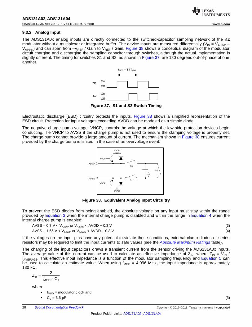
9.3.2 Analog InputThe ADS131A0x analog inputs are directly connected to the switched-capacitor sampling network of the ΔΣmodulator without a multiplexer or integrated buffer. The device inputs are measured differentially (VIN = VAINxP –VAINxN) and can span from –VREF / Gain to VREF / Gain. Figure 38 shows a conceptual diagram of the modulatorcircuit charging and discharging the sampling capacitor through switches, although the actual implementation isslightly different. The timing for switches S1 and S2, as shown in Figure 37, are 180 degrees out-of-phase of oneanother.
Figure 37. S1 and S2 Switch Timing
Electrostatic discharge (ESD) circuitry protects the inputs. Figure 38 shows a simplified representation of theESD circuit. Protection for input voltages exceeding AVDD can be modeled as a simple diode.
The negative charge pump voltage, VNCP, controls the voltage at which the low-side protection devices beginconducting. Tie VNCP to AVSS if the charge pump is not used to ensure the clamping voltage is properly set.The charge pump cannot provide a large amount of current. The mechanism shown in Figure 38 ensures currentprovided by the charge pump is limited in the case of an overvoltage event.
Figure 38. Equivalent Analog Input Circuitry
To prevent the ESD diodes from being enabled, the absolute voltage on any input must stay within the rangeprovided by Equation 3 when the internal charge pump is disabled and within the range in Equation 4 when theinternal charge pump is enabled:
AVSS – 0.3 V < VAINxP or VAINxN < AVDD + 0.3 V (3)AVSS – 1.65 V < VAINxP or VAINxN < AVDD + 0.3 V (4)
If the voltages on the input pins have any potential to violate these conditions, external clamp diodes or seriesresistors may be required to limit the input currents to safe values (see the Absolute Maximum Ratings table).
The charging of the input capacitors draws a transient current from the sensor driving the ADS131A0x inputs.The average value of this current can be used to calculate an effective impedance of ZIN, where ZIN = VIN /IAVERAGE. This effective input impedance is a function of the modulator sampling frequency and Equation 5 canbe used to calculate an estimate value. When using fMOD = 4.096 MHz, the input impedance is approximately130 kΩ.
where• fMOD = modulator clock and• CS = 3.5 pF (5)

AINxP
AINxN
VCM
AINxP
AINxN VCM
a) Psuedo-Differential Input b) Differential Input
VREF / GainPeak-to-Peak
VREF / GainPeak-to-Peak
CommonVoltage
Device
VREF / Gainto
VREF / Gain
CommonVoltage
Device
29
ADS131A02, ADS131A04www.ti.com SBAS590D –MARCH 2016–REVISED JANUARY 2018
Product Folder Links: ADS131A02 ADS131A04
Submit Documentation FeedbackCopyright © 2016–2018, Texas Instruments Incorporated
There are two general methods of driving the ADS131A0x analog inputs, as shown in Figure 39: pseudo-differential or fully-differential.
Figure 39. Pseudo-Differential and Fully-Differential Inputs
To apply a pseudo-differential signal to the fully-differential inputs, apply a dc voltage to AINxN, preferably to theanalog mid-supply [(AVDD + AVSS) / 2] or [(AVDD + VNCP) / 2] when the negative charge pump is enabled.The AINxP pins can swing between –VREF / Gain to VREF / Gain (as shown in Figure 40) around the commonvoltage. The common-mode voltage, VCM, changes with VAINxP.
Configure the signals at AINxP and AINxN to be 180° out-of-phase centered around a common-mode voltage touse a fully-differential input method. Both the AINxP and AINxN inputs swing from VCM +½ VREF / Gain to VCM –½VREF / Gain, as shown in Figure 41. The differential voltage at the maximum and minimum points is equal to VREF/ Gain to –VREF / Gain, respectively. The VCM voltage remains fixed when AINxP and AINxN swing. Use theADS131A0x in a differential configuration to maximize the dynamic range of the data converter. For optimalperformance, the VCM is recommended to be set at the midpoint of the analog supplies.
Tie any unused analog input channels directly to AVSS.
Figure 40. Pseudo-Differential Input Mode Figure 41. Fully-Differential Input Mode

AINxP
S Q
QR
+
±
ADC ADC DigitalFilter
+
±
Conversion Start Reset
StatusChannel 1
DataChannel 2
DataChannel 3
DataChannel 4
Data
Latch
CRC
COMP_TH[2:0]
S Q
QR
+
±
+
±
Conversion Start Reset
Latch
AINxN
COMP_TH[2:0]
COMP_TH[2:0]
COMP_TH[2:0]
DOUT Data Frame
30
ADS131A02, ADS131A04SBAS590D –MARCH 2016–REVISED JANUARY 2018 www.ti.com
Product Folder Links: ADS131A02 ADS131A04
Submit Documentation Feedback Copyright © 2016–2018, Texas Instruments Incorporated
9.3.3 Input Overrange and Underrange DetectionEach ADS131A0x channel has two integrated comparators to detect overrange and underrange conditions onthe input signals. Use the COMP_TH[2:0] bits in the A_SYS_CFG register to set a high and low threshold levelusing a 3-bit digital-to-analog converter (DAC). This threshold voltage is compared to the voltage on the inputpins. The voltage monitor triggers an alarm by setting the F_ADCIN bit of the STAT_1 register when theindividual voltage on AINxP or AINxN exceeds the threshold set by the COMP_TH[2:0] bits. When the F_ADCINbit of the STAT_1 register is set, indicating an out-of-range event, read the STAT_P register or STAT_N registerto determine exactly which input pin exceeded the set threshold. Figure 42 shows an input overrange andunderrange detection block diagram.
Figure 42. ADC Out-of-Range Detection Monitor
9.3.4 ReferenceThe ADS131A0x offers an integrated low-drift, 2.442-V or 4.0-V reference option. For applications that require adifferent reference voltage, the device offers a reference input option for use with an external reference voltage.
The reference source is selected by the INT_REFEN bit in the A_SYS_CFG register. By default, the externalreference is selected (INT_REFEN = 0). The internal voltage reference requires 0.2 ms to settle to 1% and 250ms to fully settle to 0.01% when switching from an external reference source to the internal reference (using therecommended bypass capacitor values). The external reference input is internally buffered to increase inputimpedance. Therefore, additional reference buffers are usually not required when using an external reference.Connect the reference voltage to the REFEXT pin when using an external reference.
External band-limiting capacitors determine the amount of reference noise contribution. For high-end systems,choose capacitor values such that the bandwidth is limited to less than 10 Hz so that the reference noise doesnot dominate the system noise. In systems with strict ADC power-on requirements, using a large capacitor on thereference increases the time for the voltage to meet the desired value, thus increasing system power-on time.Figure 43 illustrates a typical external reference drive circuitry with recommended filtering options.

REFP
REFEXT
+R1
Bandgap
REFN
AVSS
1 µF
To ADC
1 µF
INT_REFEN = 1
VREF_4V = 0
R2
R3VREF_4V = 1
AVSS
REFP
REFEXT
+
REFN
1 µF
REF50xx
VOUT
GND
AVDD
5 V
AVSS
AVSS
10 µF
AVSS
AVSS
1 µF
100
R2
R3
To ADC
31
ADS131A02, ADS131A04www.ti.com SBAS590D –MARCH 2016–REVISED JANUARY 2018
Product Folder Links: ADS131A02 ADS131A04
Submit Documentation FeedbackCopyright © 2016–2018, Texas Instruments Incorporated
NOTE: R2 = 62.3 kΩ, R3 = 97.5 kΩ.
Figure 43. External Reference Driver
Set the INTREF_EN bit to 1 in the A_SYS_CFG register to use the internal reference. When the internalreference is selected, use the VREF_4V bit to select between a 2.442-V or 4.0-V reference. By default, thedevice is set to use the 2.442-V reference. The VREF_4V bit has no function when set to use the externalreference. When enabling the negative charge pump with a 3.0-V to 3.45-V analog supply, the internal referencemust be set to 2.442 V. Figure 44 shows a simplified block diagram of the internal ADS131A0x reference. Thereference voltage is generated with respect to AVSS requiring a direct connection between REFN and AVSS.
NOTE: R1 = 20 kΩ, R2 = 62.3 kΩ, R3 = 97.5 kΩ.
Figure 44. Internal Reference

3
MOD
MOD
N fsin
fH f K
fN sin
f
ª ºS« »¬ ¼ uª ºS
u « »¬ ¼
3N
1
1 ZH z K
N 1 Z
u
u
32
ADS131A02, ADS131A04SBAS590D –MARCH 2016–REVISED JANUARY 2018 www.ti.com
Product Folder Links: ADS131A02 ADS131A04
Submit Documentation Feedback Copyright © 2016–2018, Texas Instruments Incorporated
9.3.5 ΔΣ ModulatorThe ADS131A0x is a multichannel, simultaneous sampling ΔΣ ADC where each channel has an individualmodulator and digital filter. The modulator samples the input signal at the rate of fMOD derived as a function of theADC operating clock, fICLK. As in the case of any ΔΣ modulator, the ADS131A0x noise is shaped until fMOD / 2.The modulator converts the analog input voltage into a pulse-code modulated (PCM) data stream. The on-chipdigital decimation filters take this bitstream and provide attenuation to the now shaped, higher frequency noise.This ΔΣ sample and conversion process drastically reduces the complexity of the analog antialiasing filterstypically required with nyquist ADCs.
9.3.6 Digital Decimation FilterThe digital filter receives the modulator output and decimates the data stream to create the final conversionresult. The digital filter on each channel consists of a third-order sinc filter. The oversampling ratio (OSR)determines the number of samples taken to create the output data word, and is set by the modulator rate dividedby the data rate (fMOD / fDATA). The OSR of the sinc filters is adjusted by the OSR[3:0] bits in the CLK2 register.The OSR setting is a global setting that affects all channels and, therefore, all channels operate at the same datarate in the device. By adjusting the OSR, tradeoffs can be made between noise and data rate to optimize thesignal chain: filter more for lower noise (thus creating lower data rates), filter less for higher data rates.
The sinc filter is a variable decimation rate, third-order, low-pass filter. Data are supplied to this section of thefilter from the modulator at the rate of fMOD. Equation 6 shows the scaled sinc3 filter Z-domain transfer function.As shown in Table 6, the integer N is the set OSR and the integer K is a scaling factor for OSR values that arenot an integer power of 2.
(6)
Equation 7 shows the sinc filter frequency domain transfer function. As shown in Table 6, the integer N is the setOSR and the integer K is a scaling factor for OSR values that are not an integer power of 2.
where:N = oversampling ratio (7)
Table 6. K Scaling FactorOSR (N) K SCALING VALUE
800, 400, 200 0.99837784096, 2048, 1024, 512, 256, 128, 64, 32 1.0
768, 384, 192, 96, 48 1.00195313
The sinc3 filter has notches (or zeroes) that occur at the output data rate and multiples thereof. At thesefrequencies, the filter has infinite attenuation. Figure 45 and Figure 46 illustrate the digital filter frequencyresponse out to a normalized input frequency (fIN / fDATA) of 5 and 0.5, respectively. Figure 47, Figure 48, andFigure 49 illustrate the frequency response for OSR = 32, OSR = 512, and OSR = 4096 up to fMOD, respectively.

Normalized Frequency (fIN/fDATA)
Am
plitu
de (
dB)
0 400 800 1200 1600 2000 2400 2800 3200 3600 4000-250
-225
-200
-175
-150
-125
-100
-75
-50
-25
0
D005
Normalized Frequency (fIN/fDATA)
Am
plitu
de (
dB)
0 2 4 6 8 10 12 14 16 18 20 22 24 26 28 30 32-140-130-120-110-100
-90-80-70-60-50-40-30-20-10
0
D003Normalized Frequency (fIN/fDATA)
Am
plitu
de (
dB)
0 60 120 180 240 300 360 420 480-180
-160
-140
-120
-100
-80
-60
-40
-20
0
D004
Normalized Frequency (fIN/fDATA)
Am
plitu
de (
dB)
0 0.5 1 1.5 2 2.5 3 3.5 4 4.5 5-140-130-120-110-100
-90-80-70-60-50-40-30-20-10
0
D001Normalized Frequency (fIN/fDATA)
Am
plitu
de (
dB)
0 0.1 0.2 0.3 0.4 0.5-20
-18
-16
-14
-12
-10
-8
-6
-4
-2
0
D002
33
ADS131A02, ADS131A04www.ti.com SBAS590D –MARCH 2016–REVISED JANUARY 2018
Product Folder Links: ADS131A02 ADS131A04
Submit Documentation FeedbackCopyright © 2016–2018, Texas Instruments Incorporated
Figure 45. Sinc3 Filter Frequency Response Figure 46. Sinc3 Filter Roll-Off
Figure 47. Sinc3 Filter Frequency Response (OSR 32) Figure 48. Sinc3 Filter Frequency Response (OSR 512)
Figure 49. Sinc3 Filter Frequency Response (OSR 4096)

DIN
DRDY
WAKEUP
§§
tSETTLE
ADC_ENA§
21 3
§
§
§
Normalized Frequency (fIN/fDATA)
Am
plitu
de (
dB)
0 0.01 0.02 0.03 0.04 0.05 0.06 0.07 0.08 0.09 0.1-0.5
-0.45
-0.4
-0.35
-0.3
-0.25
-0.2
-0.15
-0.1
-0.05
0
0.05
D006
OSR 512OSR 768OSR 800
34
ADS131A02, ADS131A04SBAS590D –MARCH 2016–REVISED JANUARY 2018 www.ti.com
Product Folder Links: ADS131A02 ADS131A04
Submit Documentation Feedback Copyright © 2016–2018, Texas Instruments Incorporated
The K scaling factor for OSR values that are not an integer power of two adds a non-integer gain factor to thesinc3 frequency response across all frequencies. The host must account for the K scaling factor to obtain theADC gain error given in the Electrical Characteristics table. Figure 50 overlays the digital filter frequencyresponse for the three K scaling options in Table 6. Graph scaling is set to a narrow limit to show the small gainvariation between OSR values.
Figure 50. Non-Binary OSR Sinc3 Filter Frequency ResponseThe ADS131A0x immediately begins outputting conversion data when powered up and brought out of standbymode using the WAKEUP command. The sinc3 digital filter requires three conversion cycles to provide a settledconversion result, assuming the analog input has settled to its final value (tSETTLE). The output data are not gatedwhen the digital filter settles, meaning that the first two conversion results show unsettled data from the filter pathbefore settled data are available on the third conversion cycle. The first two unsettled conversion cycles, thoughunsettled, can be used for diagnostic purposes to ensure the ADC is coming out of standby as expected.Figure 51 shows the new data ready behavior and time needed for the digital filter coming out of standby.
Figure 51. Sinc3 Filter Settling
The digital filter uses a multiple stage linear-phase digital filter. Linear -phase filters exhibit constant delay timeacross all input frequencies (also know as constant group delay). This behavior results in zero-phase error whenmeasuring multi-tone signals. For more information about group delay in delta-sigma ADCs, see the Accountingfor delay from multiple sources in delta-sigma ADCs white paper.
9.3.7 Watchdog TimerThe ADS131A0x offers an integrated watchdog timer to protect the device from entering any unresponsive state.The watchdog timer is a 16-bit counter running on an internal 50-kHz clock. The timer resets with each dataframe when the CS signal transitions from high to low. If a timer reset does not take place and the watchdogtimer expires after 500 ms, the device assumes that an unresponsive state has occurred and issues a watchdogtimer reset. Following the reset, the device enters the power-up state (see the Power-Up section), sets theF_WDT bit in the STAT_1 register, and indicates that a watchdog timer reset has taken place. Enable thewatchdog timer by setting the WDT_EN bit in the D_SYS_CFG register.
9.4 Device Functional Modes
9.4.1 Low-Power and High-Resolution ModeThe ADS131A0x offers two modes of operation: high-resolution and low-power mode. High-resolution modeenables a faster modulator clock, up to fMOD = 4.25 MHz, to maximize performance at higher data rates. Low-power mode scales the analog and digital currents and restricts the maximum fMOD to 1.05 MHz. Select theoperating mode using the HRM bit in the A_SYS_CFG register.
35
ADS131A02, ADS131A04www.ti.com SBAS590D –MARCH 2016–REVISED JANUARY 2018
Product Folder Links: ADS131A02 ADS131A04
Submit Documentation FeedbackCopyright © 2016–2018, Texas Instruments Incorporated
Device Functional Modes (continued)9.4.2 Power-UpAfter all supplies are established and the RESET pin goes high, an internal power-on-reset (POR) is performed.As part of the POR process, all registers are initialized to the default states, the state of the Mx pins are latched,the interface is placed in a locked state, and the device enters standby mode. POR can take up to 4.5 ms tocomplete. When the host communicates with the ADS131A0x, the SPI interface outputs a READY status wordindicating that the power-on cycle is completed and the device is ready to accept commands. The STAT_Sregister indicates if the ADC powered up properly or if any fault occurred during the initialization of the device.Send an UNLOCK command to enable the interface and begin communicating with the device. See Table 14 formore information on the READY status word and the UNLOCK from POR or RESET or RESET: Reset to PORValues sections for more information on bringing the device out of POR.
9.4.3 Standby and Wake-Up ModeAfter being unlocked from POR or after reset, the device enters a low-power standby mode with all ADCchannels powered down. After the registers are properly configured, enable all the ADC channels together bywriting to the ADC_ENA register and issue a WAKEUP command to start conversions. To enter standby modeagain, send the STANDBY command and disable all ADC channels by writing to the ADC_ENA register. TheADS131A0x requires using the WAKEUP and STANDBY commands together with writing to the ADC_ENAregister to disable or enable ADC channels to start and stop conversions.
9.4.4 Conversion ModeThe device runs in continuous conversion mode. When a conversion completes, the device places the result inthe output buffer and immediately begins another conversion. Data are available at the next data-ready indicator,although data may not be fully settled through the digital filter (see the Digital Decimation Filter section for moreinformation on settled data).
9.4.5 Reset (RESET)There are two methods to reset the ADS131A0x: pull the RESET pin low for at least tw(RSL) or send the RESETcommand. The RESET pin must be tied high if the RESET command is used. The RESET command takes effectat the completion of the command. As part of the reset process, all registers are initialized to the default states,the status of M0, M1, and M2 pins are latched, the interface is placed in a locked state, and the device entersstandby mode. Reset can take up to 4.5 ms to complete. The device outputs a READY status word indicatingthat the reset is completed and the device is ready to accept commands. Send an UNLOCK command to enablethe interface and begin communicating with the device. See Table 13 for more information on the READY statusword, the UNLOCK from POR command, and the RESET command. Figure 7 illustrates the critical timingrelationship of taking the ADS131A0x into reset and bringing the device out of reset.
There are two methods to reset the ADS131A0x: pull the RESET pin low, or send the RESET command. Whenusing the RESET pin, driving the pin low forces the device into reset. Follow the minimum pulse duration timingspecifications before taking the RESET pin back high. The RESET command takes effect at the completion ofthe command (see the RESET: Reset to POR Values section for more information). After the device is reset, 4.5ms are required to complete initialization of the configuration registers to the default states and for the device tobe ready for normal operation.. Figure 7 illustrates the critical timing relationship of taking the ADS131A0x intoreset and bringing the device out of reset. Tie the RESET pin high if the RESET command is used to reset thedevice.

DIN
DOUT
Data Frame
Device Word 1
Device Word 1 Device Word 3Device Word 2
Device Word 3Device Word 2
a) Frame b) Single Device Word
DIN, DOUT
SCLK §
§§
Device word is length set by M1: 16, 24, or 32 bits.
36
ADS131A02, ADS131A04SBAS590D –MARCH 2016–REVISED JANUARY 2018 www.ti.com
Product Folder Links: ADS131A02 ADS131A04
Submit Documentation Feedback Copyright © 2016–2018, Texas Instruments Incorporated
9.5 Programming
9.5.1 Interface ProtocolThe ADS131A0x is designed with an interface protocol that expands the capability of outputting more ADCsystem monitors without disrupting data flow. This protocol communicates through standard serial peripheralinterface (SPI) methods, using allocated device words within a single data transmission frame to passinformation. A single data frame starts when the interface is enabled, typically done by pulling the CS line low.The duration of a data frame is made up of several device words with programmable bit lengths. A visualrepresentation showing how a data frame is made up of multiple device words is shown in Figure 52.
Figure 52. Data Frame and Device Word
9.5.1.1 Device Word LengthThe interface is full duplex, allowing the device to be read to and written from within the same data frame. Thelength of the individual device words is programmable through the state of the M1 pin. This pin must be set toone of three states at power-up. The pin state is latched at power-up and changing the pin state after power-uphas no effect. Table 7 lists the modes associated with the M1 pin state. The M1 pin must be tied high to IOVDDthrough a < 1-kΩ resistor, low to GND through a < 1-kΩ resistor, or left floating.
Table 7. M1 Pin SettingM1 STATE DEVICE WORD LENGTH (Bits)
IOVDD 32GND 24Float 16
9.5.1.2 Fixed versus Dynamic-Frame ModeThe device has two data frame size options to set the number of device words per frame: fixed and dynamic-frame mode, controlled by the FIXED bit in the D_SYS_CFG register. By default, the ADS131A0x powers up indynamic-frame mode.
In fixed-frame mode, there are always six device words for each data frame for the ADS131A0x. The first deviceword is reserved for the status word, the next four device words are reserved for the conversion data for each ofthe four channels, and the last word is reserved for the cyclic redundancy check (CRC) data word.
In dynamic-frame mode, the number of device words per data frame is dependent on if the ADCs are enabledand if CRC data integrity is enabled. When the ADCs are powered down in standby mode, the number of devicewords per data frame is either one or two depending if CRC data integrity is enabled. In normal operation withthe ADC channels powered up, the number of device words per data frame depends on if CRC is enabled. WhenCRC data integrity is disabled in dynamic-frame mode, the sixth device word for the ADS131A0x is removedfrom the data frame. If CRC data integrity remains enabled, the device word count remains at six.

00CommandDIN
Data Frame
00 00
DOUT
00 00
Channel 1 Data
StatusChannel 2
DataChannel 3
DataChannel 4
Data00
a) Fixed-Frame Size (CRC Disabled)
00CommandDIN
Data Frame
00 00
DOUT
00
Channel 1 Data
StatusChannel 2
DataChannel 3
DataChannel 4
Data
b) Dynamic Frame Size (CRC Disabled)
00CommandDIN
Data Frame
00 00
DOUT
00 CRC
Channel 1 Data
StatusChannel 2
DataChannel 3
DataChannel 4
DataCRC
c) Fixed-Frame Size (CRC Enabled) d) Dynamic Frame Size (CRC Enabled)
00CommandDIN
Data Frame
00 00
DOUT
00 CRC
Channel 1 Data
StatusChannel 2
DataChannel 3
DataChannel 4
DataCRC
a) Fixed-Frame Size (CRC Disabled)
00CommandDIN
Data Frame
00 00
DOUT
00 CRC
00Status 00 00 00 CRC
c) Fixed-Frame Size (CRC Enabled)
CommandDIN
Data Frame
DOUT Status
b) Dynamic Frame Size (CRC Disabled)
CRCCommandDIN
Data Frame
DOUT CRCStatus
d) Dynamic Frame Size (CRC Enabled)
00CommandDIN
Data Frame
00 00
DOUT
00 00
00Status 00 00 00 00
37
ADS131A02, ADS131A04www.ti.com SBAS590D –MARCH 2016–REVISED JANUARY 2018
Product Folder Links: ADS131A02 ADS131A04
Submit Documentation FeedbackCopyright © 2016–2018, Texas Instruments Incorporated
Figure 53 shows the fixed-frame and dynamic-frame modes for the ADS131A04 in standby mode with CRC dataintegrity enabled and disabled. Figure 54 shows the fixed-frame and dynamic-frame modes for the ADS131A04with ADC channels and CRC data integrity enabled and disabled.
Figure 53. Fixed versus Dynamic-Frame Modes in Standby Mode
NOTE: CMND = Command.
Figure 54. Fixed versus Dynamic-Frame Modes With ADCs Enabled
9.5.1.3 Command WordThe command word is the first device word on every DIN data frame. This frame is reserved for sending usercommands to write or read from registers (see the SPI Command Definitions section). The commands are stand-alone, 16-bit words that appear in the 16 most significant bits (MSBs) of the first device word of the DIN dataframe. Write zeroes to the remaining unused least significant bits (LSBs) when operating in either 24-bit or 32-bitword size modes.

38
ADS131A02, ADS131A04SBAS590D –MARCH 2016–REVISED JANUARY 2018 www.ti.com
Product Folder Links: ADS131A02 ADS131A04
Submit Documentation Feedback Copyright © 2016–2018, Texas Instruments Incorporated
9.5.1.4 Status WordThe status word is the first device word in every DOUT data frame. The status word either provides a statusupdate of the ADC internal system monitors or functions as a status response to an input command; see the SPICommand Definitions section. The contents of the status word are always 16 bits in length with the remainingLSBs set to zeroes depending on the device word length; see Table 7.
9.5.1.5 Data WordsThe data words follow the status word. The device shifts individual channel data in separate data words. TheADS131A0x converter is 24-bit resolution regardless of the device word length; see Table 7. The output data aretruncated to 16 bits when using the 16-bit device word length setting (or when enabling hamming code with a 24-bit device word length setting). The output data are extended to 32 bits with eight zeroes (00000000) added tothe least significant bits when using the 32-bit device word length setting (when hamming code is disabled).
Use the device word length (see Table 7) to set the output resolution of the ADS131A0x. When placing thehardware M1 pin in a floating state, the interface operates in 16-bit device word length mode by removing theeight least significant bits. The 16 bits of data per channel are sent in binary twos complement format, MSB first.The size of one code (LSB) is calculated using Equation 8:
1 LSB = (2 × VREF / Gain) / 216 = FS / 215 (8)
A positive full-scale input [VIN ≥ (FS – 1 LSB) = (VREF / Gain – 1 LSB)] produces an output code of 7FFFh and anegative full-scale input (VIN ≤ –FS = –VREF / Gain) produces an output code of 8000h. The output clips at thesecodes for signals that exceed full-scale.
Table 8 summarizes the ideal output codes for different input signals.
(1) Excludes the effects of noise, INL, offset, and gain errors.
Table 8. 16-Bit Ideal Output Code versus Input SignalINPUT SIGNAL, VIN
VAINxP - VAINxNIDEAL OUTPUT CODE (1)
≥ FS (215 – 1) / 215 7FFFhFS / 215 0001h
0 0000h–FS / 215 FFFFh≤ –FS 8000h
Pull the M1 pin to IOVDD (through a < 1-kΩ resistor) or GND (through a < 1-kΩ resistor) to set the device eitherto a 24-bit or 32-bit device word length. In either setting, the ADS131A0x outputs 24 bits of data per channel inbinary twos complement format, MSB first. The size of one code (LSB) is calculated using Equation 9:
1 LSB = (2 × VREF / Gain) / 224 = FS / 223 (9)
A positive full-scale input [VIN ≥ (FS – 1 LSB) = (VREF / Gain – 1 LSB)] produces an output code of 7FFFFFh anda negative full-scale input (VIN ≤ –FS = –VREF / Gain) produces an output code of 800000h. The output clips atthese codes for signals that exceed full-scale.
Table 9 summarizes the ideal output codes for different input signals.
(1) Excludes the effects of noise, INL, offset, and gain errors.
Table 9. 24-Bit Ideal Output Code versus Input SignalINPUT SIGNAL, VIN
VAINxP - VAINxN IDEAL OUTPUT CODE (1)
≥ FS (223 – 1) / 223 7FFFFFhFS / 223 000001h
0 000000h–FS / 223 FFFFFFh≤ –FS 800000h

CommandDIN
Data Frame
Zero
DOUT
Zero CRC
Channel 1 Data
StatusChannel 2
DataChannel 3
DataChannel 4
DataCRC
Zero Zero
ZeroCommandDIN
Data Frame
Zero Zero
DOUT
Zero CRC
Channel 1 Data
StatusChannel 2
DataChannel 3
DataChannel 4
DataCRC
39
ADS131A02, ADS131A04www.ti.com SBAS590D –MARCH 2016–REVISED JANUARY 2018
Product Folder Links: ADS131A02 ADS131A04
Submit Documentation FeedbackCopyright © 2016–2018, Texas Instruments Incorporated
9.5.1.6 Cyclic Redundancy Check (CRC)The CRC word is the last device word in the DIN and DOUT data frame. The CRC device word is optional and isenabled by the CRC_EN control bit in the D_SYS_CFG register. When enabled, a 16-bit CRC data check wordis present in the 16 most significant bits of the last device word in the data frame on both DIN and DOUT. Usethe CRC to provide detection of single and multiple bit errors during data transmission.
The ADS131A0x implements a standard CRC16-CCITT algorithm using a polynomial of 11021h and an initialremainder of FFFFh.
The CRC on all DIN commands is verified by the device prior to command execution except for the WREGScommand; see the WREGS: Write Multiple Registers section. The WREGS command does not check the CRCprior to writing registers but does indicate if an error occurred. If the CRC on DIN is incorrect, F_CHECK in theSTAT_1 register is set to 1 and the input command does not execute (for all commands except WREGS). Fill theunused device words on DIN with zeroes, placing the CRC word in the last device word.
The number of input CRC errors is counted and stored in the error count register. The register counts errors upto 255 before rolling over to 0. The counter is cleard by reading the ERROR_CNT register.
The CRC is calculated using specific device words in the data frame determined by the CRC_MODE and FIXEDbits in the D_SYS_CFG register. For DIN, when the FIXED bit is 0, all device words are calculated into the CRC.When the FIXED bit is 1 and the CRC_MODE bit is 1, all device words are used for calculating the CRC on DIN.When the FIXED bit is 1 and the CRC_MODE bit is 0, only the command word and device words are used forthe CRC calculation on DIN.
For DOUT, when the FIXED bit is 0, all device words in the data frame are included in the CRC calculation.When the FIXED bit is 1 and CRC_MODE is 1, all device words in the data frame are included in the DOUT CRCcalculation. When the FIXED bit is 1 and CRC_MODE is 0, only the command, status word, and active devicewords are included in the DOUT CRC calculation. When hamming codes are enabled, the hamming byte of eachword is omitted in the CRC calculation.
Figure 55 and Figure 56 show which device words are included in the CRC calculation on DIN and DOUT undervarious CRC settings. In the following examples, the device words that are not checked are highlighted in red.
NOTE: CRC_MODE = 1.
Figure 55. CRC with CRC_MODE = 1
NOTE: CRC_MODE = 0.
Figure 56. CRC with CRC_MODE = 0
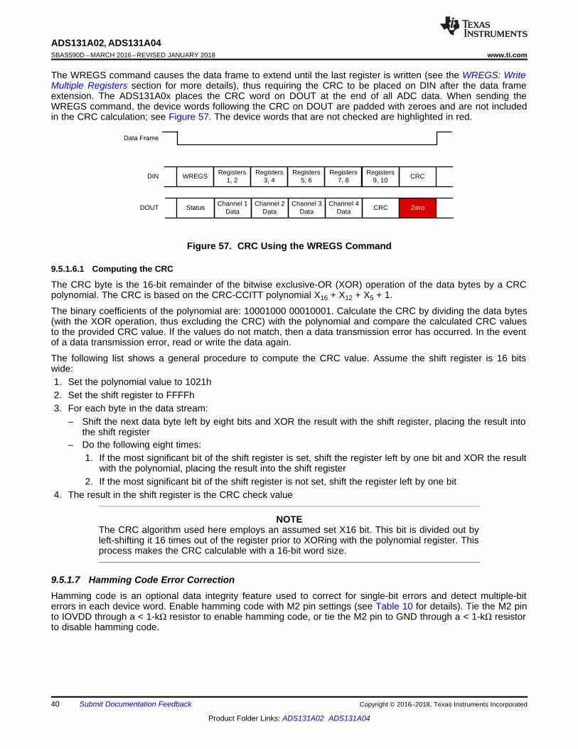
Registers1, 2
WREGSDIN
Data Frame
Registers3, 4
Registers5, 6
DOUT
Registers7, 8
Registers9, 10
CRC
Channel 1 Data
StatusChannel 2
DataChannel 3
DataChannel 4
DataCRC Zero
40
ADS131A02, ADS131A04SBAS590D –MARCH 2016–REVISED JANUARY 2018 www.ti.com
Product Folder Links: ADS131A02 ADS131A04
Submit Documentation Feedback Copyright © 2016–2018, Texas Instruments Incorporated
The WREGS command causes the data frame to extend until the last register is written (see the WREGS: WriteMultiple Registers section for more details), thus requiring the CRC to be placed on DIN after the data frameextension. The ADS131A0x places the CRC word on DOUT at the end of all ADC data. When sending theWREGS command, the device words following the CRC on DOUT are padded with zeroes and are not includedin the CRC calculation; see Figure 57. The device words that are not checked are highlighted in red.
Figure 57. CRC Using the WREGS Command
9.5.1.6.1 Computing the CRC
The CRC byte is the 16-bit remainder of the bitwise exclusive-OR (XOR) operation of the data bytes by a CRCpolynomial. The CRC is based on the CRC-CCITT polynomial X16 + X12 + X5 + 1.
The binary coefficients of the polynomial are: 10001000 00010001. Calculate the CRC by dividing the data bytes(with the XOR operation, thus excluding the CRC) with the polynomial and compare the calculated CRC valuesto the provided CRC value. If the values do not match, then a data transmission error has occurred. In the eventof a data transmission error, read or write the data again.
The following list shows a general procedure to compute the CRC value. Assume the shift register is 16 bitswide:1. Set the polynomial value to 1021h2. Set the shift register to FFFFh3. For each byte in the data stream:
– Shift the next data byte left by eight bits and XOR the result with the shift register, placing the result intothe shift register
– Do the following eight times:1. If the most significant bit of the shift register is set, shift the register left by one bit and XOR the result
with the polynomial, placing the result into the shift register2. If the most significant bit of the shift register is not set, shift the register left by one bit
4. The result in the shift register is the CRC check value
NOTEThe CRC algorithm used here employs an assumed set X16 bit. This bit is divided out byleft-shifting it 16 times out of the register prior to XORing with the polynomial register. Thisprocess makes the CRC calculable with a 16-bit word size.
9.5.1.7 Hamming Code Error CorrectionHamming code is an optional data integrity feature used to correct for single-bit errors and detect multiple-biterrors in each device word. Enable hamming code with M2 pin settings (see Table 10 for details). Tie the M2 pinto IOVDD through a < 1-kΩ resistor to enable hamming code, or tie the M2 pin to GND through a < 1-kΩ resistorto disable hamming code.

5 Hamming Bits2 ChSBits
0Bits
32-Bit ADC DataDevice Word
24 Data Bits 8 HC Bits
16 Data Bits 8 HC Bits24-Bit ADC Data
Device Word
16 Command, Status Bits 8 HC Bits
16 Command, Status Bits 8 HC Bits
32-Bit Command, StatusDevice Word
24-Bit Command, StatusDevice Word
00h
16 CRC Bits 8 HC Bits
16 CRC Bits 8 HC Bits
32-Bit CRCDevice Word
24-Bit CRCDevice Word
00h
41
ADS131A02, ADS131A04www.ti.com SBAS590D –MARCH 2016–REVISED JANUARY 2018
Product Folder Links: ADS131A02 ADS131A04
Submit Documentation FeedbackCopyright © 2016–2018, Texas Instruments Incorporated
Hamming code is only supported in 24-bit and 32-bit device word sizes. The ADS131A0x outputs 24 bits ofconversion data and an 8-bit hamming code per channel when operating in 32-bit word size. The ADS131A0xoutputs 16 bits of conversion data and an 8-bit hamming code per channel when operating in 24-bit word size.Table 10 lists the configuration options of the M1 and M2 hardware pins and the associated device word size.The status and command words are always 16 bits in length, reserving the eight least significant bits forhamming code.
Table 10. M2 Pin Setting OptionsM2 STATE M1 STATE DEVICE WORD SIZE CONVERSION DATA HAMMING DATA
IOVDDIOVDD 32 bits 24 bits On: 8 bitsGND 24 bits 16 bits On: 8 bitsFloat Not available Not available Not available
GNDIOVDD 32 bits 24 bit + 8 zeroes OffGND 24 bits 24 bit OffFloat 16 bits 16 bit Off
Float N/A Not available Not available Not available
When enabled, the hamming code byte is an additional 8-bits appended to the end of each device word on boththe input and output, as shown in Figure 58. This additional eight bits are a combination of five hamming code(Hamming) bits, two checksum (ChS) bits, and one zero bit, as shown in Figure 59.
Figure 58. Hamming Code on Each Device Word
Figure 59. Hamming Code Bit Allocation
CRC can be used with the hamming code error correction enabled. When the hamming code error correction isenabled with CRC, the 8-bit hamming data per device word is not protected by the CRC and is ignored in thecalculation. For example, if the 32-bit word size is used with hamming code enabled, the CRC check only usesthe most significant 24 bits of each device word and ignores the last eight bits used for the hamming code. TheCRC considers each device word as being 24 bits.
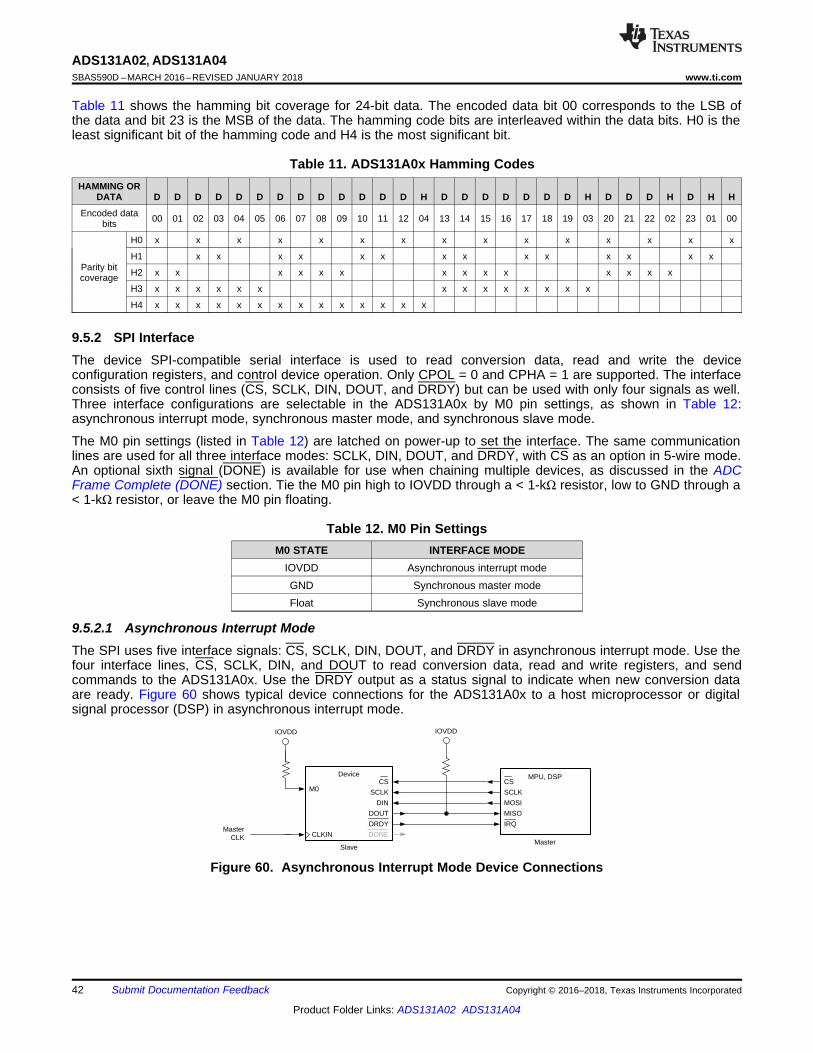
Device
M0CS
DIN
SCLK
CLKIN
MPU, DSP
IRQ
CS
MOSI
SCLK
MasterCLK
MISODOUT
DONE
DRDY
IOVDDIOVDD
SlaveMaster
42
ADS131A02, ADS131A04SBAS590D –MARCH 2016–REVISED JANUARY 2018 www.ti.com
Product Folder Links: ADS131A02 ADS131A04
Submit Documentation Feedback Copyright © 2016–2018, Texas Instruments Incorporated
Table 11 shows the hamming bit coverage for 24-bit data. The encoded data bit 00 corresponds to the LSB ofthe data and bit 23 is the MSB of the data. The hamming code bits are interleaved within the data bits. H0 is theleast significant bit of the hamming code and H4 is the most significant bit.
Table 11. ADS131A0x Hamming CodesHAMMING OR
DATA D D D D D D D D D D D D D H D D D D D D D H D D D H D H H
Encoded databits 00 01 02 03 04 05 06 07 08 09 10 11 12 04 13 14 15 16 17 18 19 03 20 21 22 02 23 01 00
Parity bitcoverage
H0 x x x x x x x x x x x x x x x
H1 x x x x x x x x x x x x x x
H2 x x x x x x x x x x x x x x
H3 x x x x x x x x x x x x x x
H4 x x x x x x x x x x x x x x
9.5.2 SPI InterfaceThe device SPI-compatible serial interface is used to read conversion data, read and write the deviceconfiguration registers, and control device operation. Only CPOL = 0 and CPHA = 1 are supported. The interfaceconsists of five control lines (CS, SCLK, DIN, DOUT, and DRDY) but can be used with only four signals as well.Three interface configurations are selectable in the ADS131A0x by M0 pin settings, as shown in Table 12:asynchronous interrupt mode, synchronous master mode, and synchronous slave mode.
The M0 pin settings (listed in Table 12) are latched on power-up to set the interface. The same communicationlines are used for all three interface modes: SCLK, DIN, DOUT, and DRDY, with CS as an option in 5-wire mode.An optional sixth signal (DONE) is available for use when chaining multiple devices, as discussed in the ADCFrame Complete (DONE) section. Tie the M0 pin high to IOVDD through a < 1-kΩ resistor, low to GND through a< 1-kΩ resistor, or leave the M0 pin floating.
Table 12. M0 Pin SettingsM0 STATE INTERFACE MODE
IOVDD Asynchronous interrupt modeGND Synchronous master modeFloat Synchronous slave mode
9.5.2.1 Asynchronous Interrupt ModeThe SPI uses five interface signals: CS, SCLK, DIN, DOUT, and DRDY in asynchronous interrupt mode. Use thefour interface lines, CS, SCLK, DIN, and DOUT to read conversion data, read and write registers, and sendcommands to the ADS131A0x. Use the DRDY output as a status signal to indicate when new conversion dataare ready. Figure 60 shows typical device connections for the ADS131A0x to a host microprocessor or digitalsignal processor (DSP) in asynchronous interrupt mode.
Figure 60. Asynchronous Interrupt Mode Device Connections
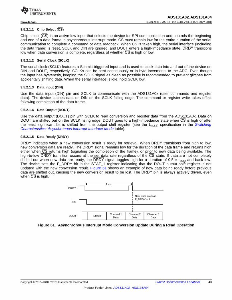
DOUT
CS
DRDY
New data are lost,F_DRDY = 1.
fDATA
Channel 1 Data
StatusChannel 2
DataChannel 3
Data
43
ADS131A02, ADS131A04www.ti.com SBAS590D –MARCH 2016–REVISED JANUARY 2018
Product Folder Links: ADS131A02 ADS131A04
Submit Documentation FeedbackCopyright © 2016–2018, Texas Instruments Incorporated
9.5.2.1.1 Chip Select (CS)
Chip select (CS) is an active-low input that selects the device for SPI communication and controls the beginningand end of a data frame in asynchronous interrupt mode. CS must remain low for the entire duration of the serialcommunication to complete a command or data readback. When CS is taken high, the serial interface (includingthe data frame) is reset, SCLK and DIN are ignored, and DOUT enters a high-impedance state. DRDY transitionslow when data conversion is complete, regardless of whether CS is high or low.
9.5.2.1.2 Serial Clock (SCLK)
The serial clock (SCLK) features a Schmitt-triggered input and is used to clock data into and out of the device onDIN and DOUT, respectively. SCLKs can be sent continuously or in byte increments to the ADC. Even thoughthe input has hysteresis, keeping the SCLK signal as clean as possible is recommended to prevent glitches fromaccidentally shifting data. When the serial interface is idle, hold SCLK low.
9.5.2.1.3 Data Input (DIN)
Use the data input (DIN) pin and SCLK to communicate with the ADS131A0x (user commands and registerdata). The device latches data on DIN on the SCLK falling edge. The command or register write takes effectfollowing completion of the data frame.
9.5.2.1.4 Data Output (DOUT)
Use the data output (DOUT) pin with SCLK to read conversion and register data from the ADS131A0x. Data onDOUT are shifted out on the SCLK rising edge. DOUT goes to a high-impedance state when CS is high or afterthe least significant bit is shifted from the output shift register (see the th(LSB) specification in the SwitchingCharacteristics: Asynchronous Interrupt Interface Mode table).
9.5.2.1.5 Data Ready (DRDY)
DRDY indicates when a new conversion result is ready for retrieval. When DRDY transitions from high to low,new conversion data are ready. The DRDY signal remains low for the duration of the data frame and returns higheither when CS returns high (signaling the completion of the frame), or prior to new data being available. Thehigh-to-low DRDY transition occurs at the set data rate regardless of the CS state. If data are not completelyshifted out when new data are ready, the DRDY signal toggles high for a duration of 0.5 × tMOD and back low.The device sets the F_DRDY bit in the STAT_1 register indicating that the DOUT output shift register is notupdated with the new conversion result. Figure 61 shows an example of new data being ready before previousdata are shifted out, causing the new conversion result to be lost. The DRDY pin is always actively driven, evenwhen CS is high.
Figure 61. Asynchronous Interrupt Mode Conversion Update During a Read Operation

Device
M0
DIN
SCLK
CLKIN
MPU, DSP
IRQ
CS
MOSI
SCLK
MasterCLK
MISODOUT
DONE
DRDY
IOVDD
CS
Master
Slave
CS
SCLK
DIN
§
§
§§
DRDY §DOUT
§§
44
ADS131A02, ADS131A04SBAS590D –MARCH 2016–REVISED JANUARY 2018 www.ti.com
Product Folder Links: ADS131A02 ADS131A04
Submit Documentation Feedback Copyright © 2016–2018, Texas Instruments Incorporated
9.5.2.1.6 Asynchronous Interrupt Mode Data Retrieval
Figure 62 shows the relationship between DRDY, CS, SCLK, DIN, and DOUT during data retrieval. The high-to-low DRDY transition indicates that new data are available. Transition CS from high to low to begin a data frame.At the end of the data frame, CS returns high and brings DRDY high.
Figure 62. DRDY Behavior with Data Retrieval in Asynchronous Interrupt Mode
9.5.2.2 Synchronous Master ModeThe SPI uses four interface signals: SCLK, DIN, DOUT, and DRDY in synchronous master mode. Connect theCS signal to the DONE signal when using a single device in synchronous master mode. The SCLK, DRDY, andDOUT signals are outputs from the device. Provide DIN from the microprocessor (MPU) or DSP using the SCLKedge timing of the ADS131A0x. Figure 63 shows typical device connections for the ADS131A0x in synchronousmaster mode to a host microprocessor or DSP.
Figure 63. Synchronous Master Mode Device Connections
9.5.2.2.1 Serial Clock (SCLK)
SCLK is the serial peripheral interface (SPI) serial clock. Use SCLK to shift in commands and shift out data fromthe device, similar to the description provided in the Asynchronous Interrupt Mode section. The SCLK outputequals the ICLK derived from the input clock, CLKIN, using the clock divider control in the CLK1 register. SCLKscontinuously output at the ICLK rate with the beginning of a data frame set by a DRDY falling edge.
9.5.2.2.2 Data Input (DIN)
Use the data input (DIN) pin and SCLK to communicate with the ADS131A0x (user commands and registerdata). The device latches data on DIN on the SCLK falling edge. The command or register write takes effectfollowing completion of the data frame.

Device
M0
DIN
SCLK
CLKIN
MPU, DSP
nIRQ
CS
MOSI
SCLK
MasterCLK
MISODOUT
DONE
DRDY
IOVDD
CSFloat
Slave
Master
SCLK
DIN
§
§
§§
DRDY
DOUT
§§
45
ADS131A02, ADS131A04www.ti.com SBAS590D –MARCH 2016–REVISED JANUARY 2018
Product Folder Links: ADS131A02 ADS131A04
Submit Documentation FeedbackCopyright © 2016–2018, Texas Instruments Incorporated
9.5.2.2.3 Data Output (DOUT)
Use the data output pin (DOUT) with SCLK to read conversion and register data from the ADS131A0x. Data onDOUT are shifted out on the SCLK rising edge. DOUT goes to a high impedance state when CS is high or afterthe least significant bit is shifted from the output shift register (see the th(LSB) specification in the SwitchingCharacteristics: Asynchronous Interrupt Interface Mode table).
9.5.2.2.4 Data Ready (DRDY)
The DRDY signal is an output that functions as a new data ready indicator and as the control for the start andstop of a data frame. A high-to-low transition of DRDY from the ADC indicates that the output shift register isupdated with new data and begins a new data frame. Subsequent SCLKs shift out the first device word onDOUT.
9.5.2.2.5 Chip Select (CS)
For single device operation in synchronous master mode, tie the CS line to the DONE output signal.
9.5.2.2.6 Synchronous Master Mode Data Retrieval
Figure 64 shows the relationship between DRDY, DOUT, DIN, and SCLK during data retrieval in synchronousmaster mode. The high-to-low DRDY transition from the ADS131A0x starts a data frame and indicates that newdata are available. DIN and DOUT transition on the SCLK rising edge. After the LSB is shifted out DRDY returnshigh, completing the data frame. The ICLK speed must be fast enough to shift out the required bits before newdata are available because ICLK determines the SCLK output rate, as described in the Serial Clock (SCLK)section. Tie the CS signal to the DONE signal in single device synchronous master mode.
Figure 64. Data Retrieval in Synchronous Master Mode
9.5.2.3 Synchronous Slave ModeThe SPI uses five interface signals: CS, SCLK, DIN, DOUT, and DRDY in synchronous slave mode. The CS,SCLK, DIN, and DRDY signals are inputs to the device and the DOUT signal is an output. DRDY can be tieddirectly to CS (for a total of four interface lines) or can be used independently as a fourth input signal forsynchronization to an external event; see the Data Ready (DRDY) section for more information on using theDRDY line for synchronization. Figure 65 shows typical device connections for the ADS131A0x in synchronousslave mode to a host microprocessor or DSP.
Figure 65. Synchronous Slave Mode Device Connections

46
ADS131A02, ADS131A04SBAS590D –MARCH 2016–REVISED JANUARY 2018 www.ti.com
Product Folder Links: ADS131A02 ADS131A04
Submit Documentation Feedback Copyright © 2016–2018, Texas Instruments Incorporated
9.5.2.3.1 Chip Select (CS)
Chip select (CS) is an active-low input that selects the device for SPI communication and controls the beginningand end of a data frame in synchronous slave mode. CS must remain low for the entire duration of the serialcommunication to complete a command or data readback. When CS is taken high, the serial interface (includingthe data frame) is reset, SCLK and DIN are ignored, and DOUT enters a high-impedance state. Tie CS directly tothe DRDY input signal to minimize communication lines as long as the synchronization timing in Figure 5 is met.Otherwise, the CS line can be used independent of DRDY.
9.5.2.3.2 Serial Clock (SCLK)
SCLK is the SPI serial clock. Use SCLK to shift in commands on DIN and shift out data from the device onDOUT, similar to the description in the Asynchronous Interrupt Mode section.
If the SCLK source is free-running, the SCLK input signal can be set as the ADC ICLK, removing the need of aseparate CLKIN. The CLKSRC bit in the CLK1 register controls the source for the ADC ICLK. The modulatorclock is derived from the ICLK using the ICLK_DIV[2:0] bits in the CLK2 register; see Figure 35 for a diagram ofhow SCLK is routed into the device when serving as the ICLK. Setting SCLK as the internal ICLK requires thatclocks are sent continuously without any delay or stop periods. Care must be taken to prevent glitches on SCLKat all times.
9.5.2.3.3 Data Input (DIN)
Use the data input pin (DIN) along with SCLK to communicate with the ADS131A0x (user commands andregister data). The device latches data on DIN on the SCLK falling edge. The command or register write takeseffect following the completion of the data frame.
9.5.2.3.4 Data Output (DOUT)
Use the data output pin (DOUT) with SCLK to read conversion and register data from the ADS131A0x. Data onDOUT are shifted out on the SCLK rising edge. DOUT goes to a high impedance state when CS is high or afterthe least significant bit is shifted from the output shift register (see the th(LSB) specification in the SwitchingCharacteristics: Asynchronous Interrupt Interface Mode table).
9.5.2.3.5 Data Ready (DRDY)
In synchronous slave mode, DRDY is an input signal that must be pulsed at the device set data rate. The DRDYinput signal is compared to an internally-generated data update signal to verify that these two signals aresynchronized. A high-to-low DRDY transition is expected at the programmed data rate or at multiples thereof. Inthe event of an unexpected DRDY input pulse, the F_RESYNC bit flags in the STAT_1 register and the ADCdigital filter resets. Use the DRDY input signal as a synchronization method to align new data ready with anexternal event or with a second ADS131A0x device. See the Timing Requirements: Synchronous Slave InterfaceMode table for the timing requirements of the DRDY input in synchronous slave mode.
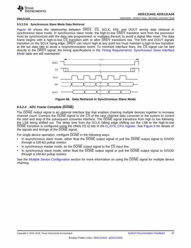
CS
SCLK
DIN
DRDY
DOUT
tDATA
47
ADS131A02, ADS131A04www.ti.com SBAS590D –MARCH 2016–REVISED JANUARY 2018
Product Folder Links: ADS131A02 ADS131A04
Submit Documentation FeedbackCopyright © 2016–2018, Texas Instruments Incorporated
9.5.2.3.6 Synchronous Slave Mode Data Retrieval
Figure 66 shows the relationship between DRDY, CS, SCLK, DIN, and DOUT during data retrieval insynchronous slave mode. In synchronous slave mode, the high-to-low DRDY transition sent from the processormust be synchronized with the data rate programmed, or multiples thereof, to avoid a digital filter reset. The dataframe begins with a high-to-low CS transition with or after DRDY transitions low. The DIN and DOUT signalstransition on the SCLK rising edge. DRDY can return high at any point but must maintain a high-to-low transitionat the set data rate to avoid a resynchronization event. To minimize interface lines, the CS signal can be tieddirectly to the DRDY signal; the timing specifications in the Timing Requirements: Synchronous Slave InterfaceMode table are still maintained.
Figure 66. Data Retrieval in Synchronous Slave Mode
9.5.2.4 ADC Frame Complete (DONE)The DONE output signal is an optional interface line that enables chaining multiple devices together to increasechannel count. Connect the DONE signal to the CS of the next chained data converter in the system to controlthe start and stop of the subsequent converter interface. The DONE signal transitions from high to low followingthe LSB being shifted out. The delay time from the SCLK falling edge shifting out the LSB to the high-to-lowDONE transition is configured using the DNDLY[1:0] bits in the D_SYS_CFG register. See Figure 6 for details ofthe signals and timings of the DONE signal.
For single device operation, configure DONE in the following ways:• In asynchronous slave mode, either float the DONE output signal or pull the DONE output signal to IOVDD
through a 100-kΩ pullup resistor.• In synchronous master mode, tie the DONE output signal to the CS input line.• In synchronous slave mode, either float the DONE output signal or pull the DONE output signal to IOVDD
through a 100-kΩ pullup resistor.
See the Multiple Device Configuration section for more information on using the DONE signal for multiple devicechaining.

48
ADS131A02, ADS131A04SBAS590D –MARCH 2016–REVISED JANUARY 2018 www.ti.com
Product Folder Links: ADS131A02 ADS131A04
Submit Documentation Feedback Copyright © 2016–2018, Texas Instruments Incorporated
9.5.3 SPI Command DefinitionsThe ADS131A0x device operation is controlled and configured through ten commands. Table 13 summarizes theavailable commands. The commands are stand-alone, 16-bit words and reside in the first device word of the dataframe. Write zeroes to the remaining LSBs when operating in either 24-bit or 32-bit word sizes because eachcommand is 16-bits in length. The commands are decoded following the completion of a data frame and takeeffect immediately. Each recognized command is acknowledged with a status output in the first device word ofthe next data frame.
Table 13. Command Definitions
COMMAND DESCRIPTION DEVICE WORDADDITIONAL
DEVICE WORD
COMMANDSTATUS
RESPONSESYSTEM COMMANDSNULL Null command 0000h STATUSRESET Software reset 0011h READYSTANDBY Enter low-power standby mode 0022h ACK = 0022hWAKEUP Wake-up from standby mode 0033h ACK = 0033h
LOCKPlaces the interface in a locked state andignores all commands except NULL, RREGS,and UNLOCK
0555h ACK = 0555h
UNLOCK Brings the device out of an unconfigured PORstate or a locked state 0655h ACK = 0655h
REGISTER WRITE AND READ COMMANDS
RREG Read a single register (001a aaaa nnnnnnnn)b REG
RREGS Read (nnnn nnnn + 1) registers starting ataddress a aaaa
(001a aaaa nnnnnnnn)b RREGS
WREG Write a single register at address a aaaa withdata dddd dddd
(010a aaaa dddddddd)b
REG (updatedregister)
WREGS
Write (nnnn nnnn + 1) registers beginning ataddress a aaaa. Additional device words arerequired to send data (dddd dddd) to registeraddress (a) and data (eeee eeee) to registeraddress (a+1). Each device word contains datafor two registers.The data frame size is extended by (n / 2) devicewords to allow for command completion.
(011a aaaa nnnnnnnn)b
(dddd dddd eeeeeeee)b
ACK =(010a_aaaa_nnnn_n
nnn)b
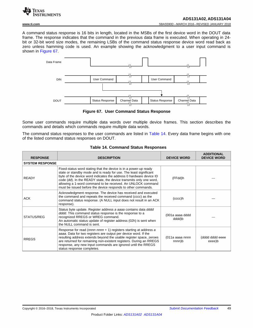
DIN
DOUT
Data Frame
User Command
Status Response Channel Data
User Command
Status Response Channel Data
49
ADS131A02, ADS131A04www.ti.com SBAS590D –MARCH 2016–REVISED JANUARY 2018
Product Folder Links: ADS131A02 ADS131A04
Submit Documentation FeedbackCopyright © 2016–2018, Texas Instruments Incorporated
A command status response is 16 bits in length, located in the MSBs of the first device word in the DOUT dataframe. The response indicates that the command in the previous data frame is executed. When operating in 24-bit or 32-bit word size modes, the remaining LSBs of the command status response device word read back aszero unless hamming code is used. An example showing the acknowledgment to a user input command isshown in Figure 67.
Figure 67. User Command Status Response
Some user commands require multiple data words over multiple device frames. This section describes thecommands and details which commands require multiple data words.
The command status responses to the user commands are listed in Table 14. Every data frame begins with oneof the listed command status responses on DOUT.
Table 14. Command Status Responses
RESPONSE DESCRIPTION DEVICE WORDADDITIONAL
DEVICE WORDSYSTEM RESPONSE
READY
Fixed-status word stating that the device is in a power-up readystate or standby mode and is ready for use. The least significantbyte of the device word indicates the address 0 hardware device IDcode (dd). In the READY state, the device transmits only one word,allowing a 1-word command to be received. An UNLOCK commandmust be issued before the device responds to other commands.
(FFdd)h —
ACK
Acknowledgment response. The device has received and executedthe command and repeats the received command (cccc) as thecommand status response. (A NULL input does not result in an ACKresponse).
(cccc)h —
STATUS/REG
Status byte update. Register address a aaaa contains data dddddddd. This command status response is the response to arecognized RREGS or WREG command.An automatic status update of register address (02h) is sent whenthe NULL command is sent.
(001a aaaa dddddddd)b —
RREGS
Response for read (nnnn nnnn + 1) registers starting at address aaaaa. Data for two registers are output per device word. If theresulting address extends beyond the usable register space, zeroesare returned for remaining non-existent registers. During an RREGSresponse, any new input commands are ignored until the RREGSstatus response completes.
(011a aaaa nnnnnnnn)b
(dddd dddd eeeeeeee)b

DIN
DOUT
Data Frame
STANDBY (0022h)
StatusResponse
Channel Data
User Command
ACK (0022h)Status
ResponseREG
(STAT_1)
NULLWAKEUP(0033h)
Standby Standby Standby
DIN
DOUT
Data Frame
RESET (0011h)
Status Response Channel Data
NULL
READY (FFxx)
Locked StateReset Delay
DIN
DOUT
Data Frame
NULL (0000h)
Status Response Channel Data
User Command
Channel DataREG(STAT_1)
50
ADS131A02, ADS131A04SBAS590D –MARCH 2016–REVISED JANUARY 2018 www.ti.com
Product Folder Links: ADS131A02 ADS131A04
Submit Documentation Feedback Copyright © 2016–2018, Texas Instruments Incorporated
9.5.3.1 NULL: Null CommandThe NULL command has no effect on ADC registers or data. Rather than producing an ACK response on DOUT,the command issues a register readback of the STAT_1 register to monitor for general fault updates. An exampleof the response to a NULL command is shown in Figure 68.
Figure 68. NULL Command Status Response
9.5.3.2 RESET: Reset to POR ValuesThe RESET command places the ADC into a power-on reset (POR) state, resetting all user registers to thedefault states. The reset begins following the completion of the frame. When reset completes, the ADC enters areset locked state and outputs the READY status response on DOUT as the command status response. Anexample of the response to a RESET command is shown in Figure 69.
Figure 69. RESET Command Status Response
9.5.3.3 STANDBY: Enter Standby ModeThe STANDBY command places the ADC in a low-power standby mode, halting conversions. The digitalinterface remains powered, allowing all registers to retain the previous states. When in standby mode, writingand reading from registers is possible and any programmable bits that activate circuitry take effect in the deviceafter the WAKEUP command is issued. The command status response following a STANDBY command is0022h. In standby mode, the command status response is dependent on the user command that is sent. All ADCchannels must be disabled (by writing to the ADCx registers) prior to entering standby mode to reduce currentconsumption. An example for the response to the STANDBY command and behavior when in standby mode isshown in Figure 70.
Figure 70. STANDBY Command Status Response

DIN
DOUT
Data Frame
NULL
ACK (STAT_1) DataACK (0655h)
Locked
Data Data
UNLOCK (0655h)
ACK (STAT_1)
Locked Unlocked
User Command
DIN
DOUT
Data Frame
Status Response
LOCK (0555h)
ACK (STAT_1) DataACK (0555h)
Locked Locked
Data Data
NULL NULL
DIN
DOUT
Data Frame
RREG (STAT_1)
NULL WAKEUP (0033h)
Standby
ACK (0033h) DataRREG (STAT_1)
Standby Normal
51
ADS131A02, ADS131A04www.ti.com SBAS590D –MARCH 2016–REVISED JANUARY 2018
Product Folder Links: ADS131A02 ADS131A04
Submit Documentation FeedbackCopyright © 2016–2018, Texas Instruments Incorporated
9.5.3.4 WAKEUP: Exit STANDBY ModeThe WAKEUP command brings the ADC out of standby mode. The ADC channels must be enabled (by writing tothe ADCx registers) before bringing the device out of standby mode. Allow enough time for all circuits in standbymode to power-up (see the Electrical Characteristics table for details). The command status response following aWAKEUP command is 0033h. An example showing the response to exiting standby mode using the WAKEUPcommand is shown in Figure 71.
Figure 71. WAKEUP Command Status Response
9.5.3.5 LOCK: Lock ADC RegistersThe LOCK command places the converter interface in a locked state where the interface becomes unresponsiveto most input commands. The UNLOCK, NULL, RREG, and RREGS commands are the only commands that arerecognized when reading back data. Following the LOCK command, the first DOUT status response reads 0555hfollowed by the command status response of a NULL command (by reading the STAT_1 register). An exampleshowing the response to sending a LOCK command and entering a register locked state is shown in Figure 72.
Figure 72. LOCK Command Status Response
9.5.3.6 UNLOCK: Unlock ADC RegistersThe UNLOCK command brings the converter out of the locked state, allowing all registers to be accessed in thenext data frame. The command status response associated with the UNLOCK command is 0655h. An exampleof bringing the interface out of the locked state using the UNLOCK command is shown in Figure 73.
Figure 73. UNLOCK Command Status Response

DIN
DOUT
Data Frame
RREG REG(a)
Status Word Data
RREG REG(b)
REG(a) Data DataREG(b)
NULL
DIN
DOUT
Data Frame
NULL
READY (FFxx) DataACK (0655h)
Locked
UNLOCK (0655h)
READY (FFxx)
Locked Unlocked
User Command
POR_EVENT
POR_EVENT
POR_EVENT
52
ADS131A02, ADS131A04SBAS590D –MARCH 2016–REVISED JANUARY 2018 www.ti.com
Product Folder Links: ADS131A02 ADS131A04
Submit Documentation Feedback Copyright © 2016–2018, Texas Instruments Incorporated
9.5.3.6.1 UNLOCK from POR or RESET
When powering up the device or coming out of a power-on reset (POR) state, the ADC does not accept anycommands. During this time, the jost can poll the ADC until the command status response reads back FFDDh(DD denotes the channel count defined by the NU_CH[3:0] bits in the ID_MSB register), indicating that the ADCpower-on reset cycle is complete and that the ADC is ready to accept commands. Use the UNLOCK commandto enable the SPI interface and begin communication with the device. The command status response associatedwith the UNLOCK command is 0655h. Figure 74 shows an example of unlocking the device after POR using theUNLOCK command.
Figure 74. UNLOCK from a POR Command Status Response
9.5.3.7 RREG: Read a Single RegisterThe RREG command reads register data from the ADC. RREG is a 16-bit command containing the command,the register address, and the number of registers to be to read. The command details are shown below:
First byte: 001a aaaa, where a aaaa is the register addressSecond byte: 00h
The ADC executes the command upon completion of the data frame and the register data transmission beginson the first device word of the following data frame. The response contains an 8-bit acknowledgement byte withthe register address and an 8-bit data byte with the register content. Figure 75 shows an example commandresponse to a single register read.
Figure 75. RREGS Command Status Response (Single Register Read)
9.5.3.8 RREGS: Read Multiple RegistersFor a multiple register read back, the command status response exceeds the 16-bit reserved device word space,causing an overflow to additional command status words. The first command status response is anacknowledgment of multiple registers to be read back and the additional command status responses shift outregister data. The command status response details are shown below:
First command status response: 001a aaaa nnnn nnnn, where a aaaa is the starting register address andnnnn nnnn is the number of registers to read minus one (n-1).Additional command status responses: dddd dddd eeee eeee , where dddd dddd is the register data from thefirst register read back and eeee eeee is the register data from the second read back register.
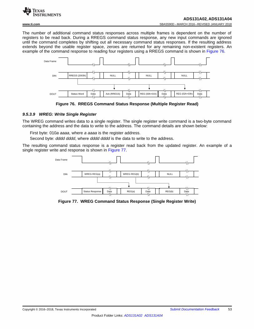
DIN
DOUT
Data Frame
WREG REG(a)
Status Response Data
WREG REG(b)
REG(a) Data DataREG(b)
NULL
DIN
DOUT
Data Frame
RREGS (2003h)
Status Word Data
NULL
Ack (RREGS) Data Data DataREG (00h+01h) REG (02h+03h)
NULL NULL
53
ADS131A02, ADS131A04www.ti.com SBAS590D –MARCH 2016–REVISED JANUARY 2018
Product Folder Links: ADS131A02 ADS131A04
Submit Documentation FeedbackCopyright © 2016–2018, Texas Instruments Incorporated
The number of additional command status responses across multiple frames is dependent on the number ofregisters to be read back. During a RREGS command status response, any new input commands are ignoreduntil the command completes by shifting out all necessary command status responses. If the resulting addressextends beyond the usable register space, zeroes are returned for any remaining non-existent registers. Anexample of the command response to reading four registers using a RREGS command is shown in Figure 76.
Figure 76. RREGS Command Status Response (Multiple Register Read)
9.5.3.9 WREG: Write Single RegisterThe WREG command writes data to a single register. The single register write command is a two-byte commandcontaining the address and the data to write to the address. The command details are shown below:
First byte: 010a aaaa, where a aaaa is the register address.Second byte: dddd dddd, where dddd dddd is the data to write to the address.
The resulting command status response is a register read back from the updated register. An example of asingle register write and response is shown in Figure 77.
Figure 77. WREG Command Status Response (Single Register Write)

DIN
DOUT
Data Frame
WREGSCommand
NULL
Status Response
REG (a+b) REG (c+d) REG (m+n)
WREGSResponse
Channel 1 Data Channel 2 Data 00h DataData
54
ADS131A02, ADS131A04SBAS590D –MARCH 2016–REVISED JANUARY 2018 www.ti.com
Product Folder Links: ADS131A02 ADS131A04
Submit Documentation Feedback Copyright © 2016–2018, Texas Instruments Incorporated
9.5.3.10 WREGS: Write Multiple RegistersThe WREGS command writes data to multiple registers. The command steps through each registerincrementally, thus allowing the user to incrementally write to each register. This process extends the data frameby (n) device words to complete the command. If the resulting address extends beyond the usable registerspace, any following data for non-existent registers are ignored. The 16 bits contained in the first device wordcontain the command, the starting register address, and the number of registers to write, followed by additionaldevice words for the register data. The command details are shown below:
First user command device word: 011a aaaa nnnn nnnn, where a aaaa is the starting register address andnnnn nnnn is the number of registers to write minus one (n-1).Additional user command device words: dddd dddd eeee eeee, where dddd dddd is the data to write to thefirst register and eeee eeee is the register data for the second register.
The user command device word uses the 16 MSBs regardless of word length (that is, only the 16 MSBs areused in 16-bit, 24-bit, or 32-bit word lengths). When additional command device words are required, only amaximum of two 8-bit registers can be written per command and any additional LSBs beyond 16 bits are ignored.The command status response for the WREGS command is 010a aaaa nnnn nnnn, where a aaaa is the startingregister address and nnnn nnnn is the number of registers written minus one. An example of a multiple registerwrite and the command status response is shown in Figure 78.
Figure 78. WREGS Command Status Response (Multiple Register Write)
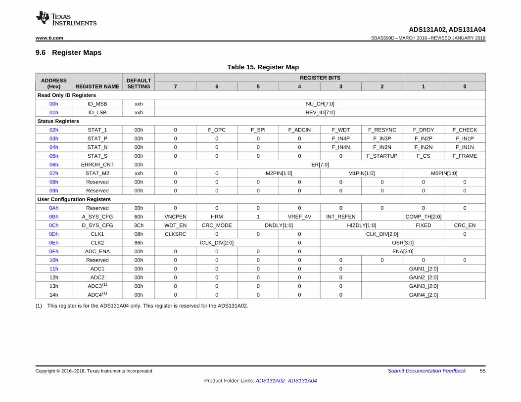
ADS131A02, ADS131A04www.ti.com SBAS590D –MARCH 2016–REVISED JANUARY 2018
55
Product Folder Links: ADS131A02 ADS131A04
Submit Documentation FeedbackCopyright © 2016–2018, Texas Instruments Incorporated
(1) This register is for the ADS131A04 only. This register is reserved for the ADS131A02.
9.6 Register Maps
Table 15. Register Map
ADDRESS(Hex) REGISTER NAME
DEFAULTSETTING
REGISTER BITS7 6 5 4 3 2 1 0
Read Only ID Registers00h ID_MSB xxh NU_CH[7:0]01h ID_LSB xxh REV_ID[7:0]
Status Registers02h STAT_1 00h 0 F_OPC F_SPI F_ADCIN F_WDT F_RESYNC F_DRDY F_CHECK03h STAT_P 00h 0 0 0 0 F_IN4P F_IN3P F_IN2P F_IN1P04h STAT_N 00h 0 0 0 0 F_IN4N F_IN3N F_IN2N F_IN1N05h STAT_S 00h 0 0 0 0 0 F_STARTUP F_CS F_FRAME06h ERROR_CNT 00h ER[7:0]07h STAT_M2 xxh 0 0 M2PIN[1:0] M1PIN[1:0] M0PIN[1:0]08h Reserved 00h 0 0 0 0 0 0 0 009h Reserved 00h 0 0 0 0 0 0 0 0
User Configuration Registers0Ah Reserved 00h 0 0 0 0 0 0 0 00Bh A_SYS_CFG 60h VNCPEN HRM 1 VREF_4V INT_REFEN COMP_TH[2:0]0Ch D_SYS_CFG 3Ch WDT_EN CRC_MODE DNDLY[1:0] HIZDLY[1:0] FIXED CRC_EN0Dh CLK1 08h CLKSRC 0 0 0 CLK_DIV[2:0] 00Eh CLK2 86h ICLK_DIV[2:0] 0 OSR[3:0]0Fh ADC_ENA 00h 0 0 0 0 ENA[3:0]10h Reserved 00h 0 0 0 0 0 0 0 011h ADC1 00h 0 0 0 0 0 GAIN1_[2:0]12h ADC2 00h 0 0 0 0 0 GAIN2_[2:0]13h ADC3 (1) 00h 0 0 0 0 0 GAIN3_[2:0]14h ADC4 (1) 00h 0 0 0 0 0 GAIN4_[2:0]
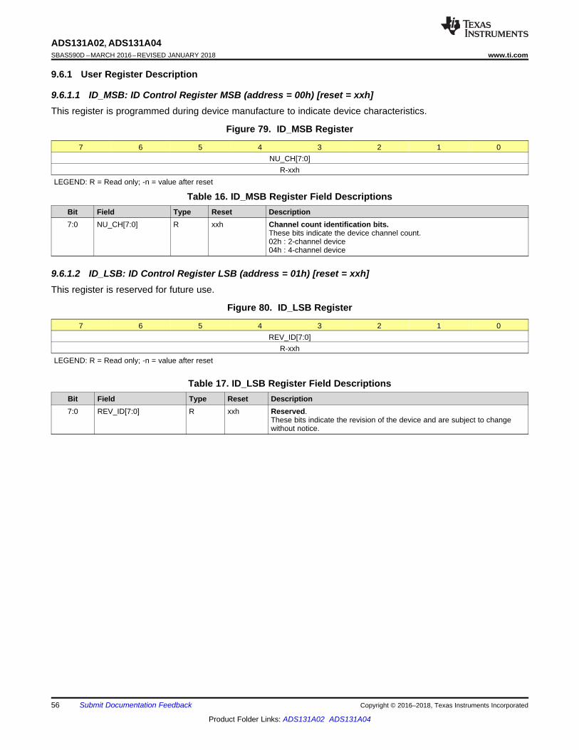
56
ADS131A02, ADS131A04SBAS590D –MARCH 2016–REVISED JANUARY 2018 www.ti.com
Product Folder Links: ADS131A02 ADS131A04
Submit Documentation Feedback Copyright © 2016–2018, Texas Instruments Incorporated
9.6.1 User Register Description
9.6.1.1 ID_MSB: ID Control Register MSB (address = 00h) [reset = xxh]This register is programmed during device manufacture to indicate device characteristics.
Figure 79. ID_MSB Register
7 6 5 4 3 2 1 0NU_CH[7:0]
R-xxhLEGEND: R = Read only; -n = value after reset
Table 16. ID_MSB Register Field DescriptionsBit Field Type Reset Description7:0 NU_CH[7:0] R xxh Channel count identification bits.
These bits indicate the device channel count.02h : 2-channel device04h : 4-channel device
9.6.1.2 ID_LSB: ID Control Register LSB (address = 01h) [reset = xxh]This register is reserved for future use.
Figure 80. ID_LSB Register
7 6 5 4 3 2 1 0REV_ID[7:0]
R-xxhLEGEND: R = Read only; -n = value after reset
Table 17. ID_LSB Register Field DescriptionsBit Field Type Reset Description7:0 REV_ID[7:0] R xxh Reserved.
These bits indicate the revision of the device and are subject to changewithout notice.

57
ADS131A02, ADS131A04www.ti.com SBAS590D –MARCH 2016–REVISED JANUARY 2018
Product Folder Links: ADS131A02 ADS131A04
Submit Documentation FeedbackCopyright © 2016–2018, Texas Instruments Incorporated
9.6.1.3 STAT_1: Status 1 Register (address = 02h) [reset = 00h]This register contains general fault updates. This register is automatically transferred on the command statusresponse when the NULL command is sent.
Figure 81. STAT_1 Register
7 6 5 4 3 2 1 00 F_OPC F_SPI F_ADCIN F_WDT F_RESYNC F_DRDY F_CHECK
R-0h R-0h R-0h R-0h R-0h R-0h R-0h R-0hLEGEND: R = Read only; -n = value after reset
Table 18. STAT_1 Register Field DescriptionsBit Field Type Reset Description7 Reserved R 0h Reserved.
Always read 0.6 F_OPC R 0h Command fault.
This bit indicates that a received command is not recognized as valid andthe command is ignored. This bit auto-clears on a STAT_1 data transfer,unless the condition remains.When in a locked state, this bit is set if any command other than LOCK,UNLOCK, NULL, or RREGS is written to the device.0 : No fault has occurred1 : Possible invalid command is ignored
5 F_SPI R 0h SPI fault.This bit indicates that one of the status bits in the STAT_S register is set.Read the STAT_S register to clear the bit.0 : No fault has occurred1 : A bit in the STAT_S register is set high
4 F_ADCIN R 0h ADC input fault.This bit indicates that one of the ADC input fault detection bits in theSTAT_P or STAT_N register is set. Read the STAT_P and STAT_Nregisters to clear the bit.0 : No fault has occurred1 : A bit in the STAT_P or STAT_N register is set high
3 F_WDT R 0h Watchdog timer timeout.This bit indicates if the watchdog timer times out before a new data frametransfer occurs.0 : No fault has occurred1 : Timer has run out (resets following register read back)
2 F_RESYNC R 0h Resynchronization fault.This bit is set whenever the signal path is momentarily reset resulting froma DRDY synchronization event. This fault is only possible in synchronousslave mode.0 : Devices are in sync1 : Signal path is momentarily reset to maintain synchronization
1 F_DRDY R 0h Data ready fault.This bit is set if data shifted out from the previous result are not completeby the time new ADC data are ready. The ADC DRDY line pulses,indicating that new data are available and overwrite the current data. Thisbit auto-clears on a STAT_1 transfer, unless the condition remains.0 : Data read back complete before new data update1 : New data update during DOUT data transmission
0 F_CHECK R 0h DIN check fault.This bit is set if either of the following conditions are detected:• Uncorrectable hamming error correction state is determined for any
DIN word transfer when hamming code is enabled.• CRC check word on DIN fails. The input command that triggered this
error is ignored.This bit auto-clears on a STAT_S transfer, unless the condition remains.0 : No error in DIN transmission1 : DIN transmission error
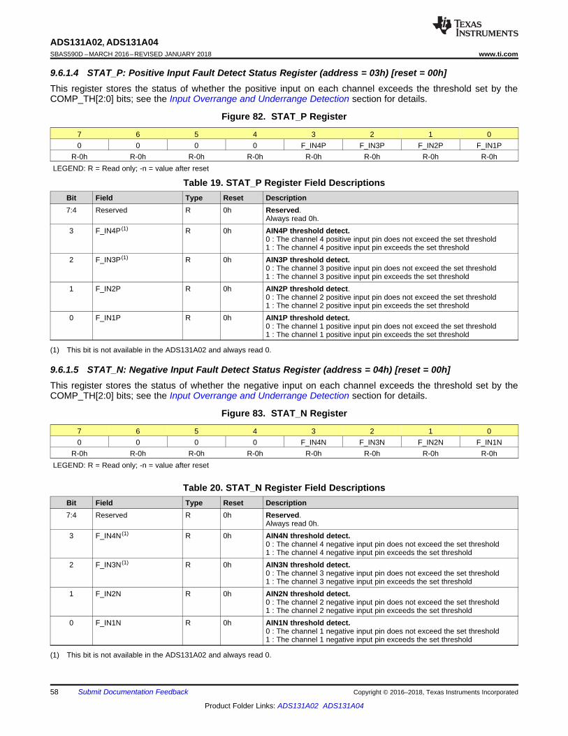
58
ADS131A02, ADS131A04SBAS590D –MARCH 2016–REVISED JANUARY 2018 www.ti.com
Product Folder Links: ADS131A02 ADS131A04
Submit Documentation Feedback Copyright © 2016–2018, Texas Instruments Incorporated
9.6.1.4 STAT_P: Positive Input Fault Detect Status Register (address = 03h) [reset = 00h]This register stores the status of whether the positive input on each channel exceeds the threshold set by theCOMP_TH[2:0] bits; see the Input Overrange and Underrange Detection section for details.
Figure 82. STAT_P Register
7 6 5 4 3 2 1 00 0 0 0 F_IN4P F_IN3P F_IN2P F_IN1P
R-0h R-0h R-0h R-0h R-0h R-0h R-0h R-0hLEGEND: R = Read only; -n = value after reset
(1) This bit is not available in the ADS131A02 and always read 0.
Table 19. STAT_P Register Field DescriptionsBit Field Type Reset Description7:4 Reserved R 0h Reserved.
Always read 0h.3 F_IN4P (1) R 0h AIN4P threshold detect.
0 : The channel 4 positive input pin does not exceed the set threshold1 : The channel 4 positive input pin exceeds the set threshold
2 F_IN3P (1) R 0h AIN3P threshold detect.0 : The channel 3 positive input pin does not exceed the set threshold1 : The channel 3 positive input pin exceeds the set threshold
1 F_IN2P R 0h AIN2P threshold detect.0 : The channel 2 positive input pin does not exceed the set threshold1 : The channel 2 positive input pin exceeds the set threshold
0 F_IN1P R 0h AIN1P threshold detect.0 : The channel 1 positive input pin does not exceed the set threshold1 : The channel 1 positive input pin exceeds the set threshold
9.6.1.5 STAT_N: Negative Input Fault Detect Status Register (address = 04h) [reset = 00h]This register stores the status of whether the negative input on each channel exceeds the threshold set by theCOMP_TH[2:0] bits; see the Input Overrange and Underrange Detection section for details.
Figure 83. STAT_N Register
7 6 5 4 3 2 1 00 0 0 0 F_IN4N F_IN3N F_IN2N F_IN1N
R-0h R-0h R-0h R-0h R-0h R-0h R-0h R-0hLEGEND: R = Read only; -n = value after reset
(1) This bit is not available in the ADS131A02 and always read 0.
Table 20. STAT_N Register Field DescriptionsBit Field Type Reset Description7:4 Reserved R 0h Reserved.
Always read 0h.3 F_IN4N (1) R 0h AIN4N threshold detect.
0 : The channel 4 negative input pin does not exceed the set threshold1 : The channel 4 negative input pin exceeds the set threshold
2 F_IN3N (1) R 0h AIN3N threshold detect.0 : The channel 3 negative input pin does not exceed the set threshold1 : The channel 3 negative input pin exceeds the set threshold
1 F_IN2N R 0h AIN2N threshold detect.0 : The channel 2 negative input pin does not exceed the set threshold1 : The channel 2 negative input pin exceeds the set threshold
0 F_IN1N R 0h AIN1N threshold detect.0 : The channel 1 negative input pin does not exceed the set threshold1 : The channel 1 negative input pin exceeds the set threshold

59
ADS131A02, ADS131A04www.ti.com SBAS590D –MARCH 2016–REVISED JANUARY 2018
Product Folder Links: ADS131A02 ADS131A04
Submit Documentation FeedbackCopyright © 2016–2018, Texas Instruments Incorporated
9.6.1.6 STAT_S: SPI Status Register (address = 05h) [reset = 00h]This register indicates the detection of SPI fault conditions.
Figure 84. STAT_S Register
7 6 5 4 3 2 1 00 0 0 0 0 F_STARTUP F_CS F_FRAME
R-0h R-0h R-0h R-0h R-0h R-0h R-0h R-0hLEGEND: R = Read only; -n = value after reset
Table 21. STAT_S Register Field DescriptionsBit Field Type Reset Description7:3 Reserved R 00h Reserved.
Always read 00h.2 F_STARTUP R 0h ADC startup fault.
This bit indicates if an error is detected during power-up. This bit clearsonly when power is recycled.0 : No fault has occurred1 : A fault has occurred
1 F_CS R 0h Chip-select fault.This bit is set if CS transitions when the SCLK pin is high. This bit auto-clears on a STAT_S transfer, unless the condition remains.0 : CS is asserted or deasserted when SCLK is low1 : CS is asserted or deasserted when SCLK is high
0 F_FRAME R 0h Frame fault.This bit is set if the device detects that not enough SCLK cycles are sent ina data frame for the existing mode of operation. This bit auto-clears on aSTAT_S transfer, unless the condition remains.0 : Enough SCLKs are sent per frame1 : Not enough SCLKs are sent per frame
9.6.1.7 ERROR_CNT: Error Count Register (address = 06h) [reset = 00h]This register counts the hamming and CRC errors. This register is cleared when read.
Figure 85. ERROR_CNT Register
7 6 5 4 3 2 1 0ER7 ER6 ER5 ER4 ER3 ER2 ER1 ER0R-0h R-0h R-0h R-0h R-0h R-0h R-0h R-0h
LEGEND: R = Read only; -n = value after reset
Table 22. ERROR_CNT Register Field DescriptionsBit Field Type Reset Description7:0 ER[7:0] R 00h Error tracking count.
These bits count the number of hamming and CRC errors on the input. Thecounter saturates if the number of errors exceeds 255, FFh. This register iscleared when read.

60
ADS131A02, ADS131A04SBAS590D –MARCH 2016–REVISED JANUARY 2018 www.ti.com
Product Folder Links: ADS131A02 ADS131A04
Submit Documentation Feedback Copyright © 2016–2018, Texas Instruments Incorporated
9.6.1.8 STAT_M2: Hardware Mode Pin Status Register (address = 07h) [reset = xxh]This register indicates detection of the captured states of the hardware mode pins.
(1) Reset values are dependent on the state of the hardware pin.
Figure 86. STAT_M2 Register
7 6 5 4 3 2 1 00 0 M2PIN[1:0] M1PIN[1:0] M0PIN[1:0]
R-0h R-0h R-xh (1) R-xh (1) R-xh (1)
LEGEND: R = Read only; -n = value after reset
(1) Reset values are dependent on the state of the hardware pin.
Table 23. STAT_M2 Register Field DescriptionsBit Field Type Reset Description7:6 Reserved R 0h Reserved.
Always read 0h.5:4 M2PIN[1:0] R xh (1) M2 captured state.
These bits indicate the captured state of the M2 hardware control pin.00 : GND (hamming code word validation off)01 : IOVDD (hamming code word validation on)10 : No connection11 : Reserved
3:2 M1PIN[1:0] R xh (1) M1 captured state.These bits indicate the captured state of the M1 hardware control pin.00 : GND (24-bit device word)01 : IOVDD (32-bit device word)10 : No connection (16-bit device word)11 : Reserved
1:0 M0PIN[1:0] R xh (1) M0 captured state.These bits indicate the captured state of the M0 hardware control pin.00 : GND (synchronous master mode)01 : IOVDD (asynchronous slave mode )10 : No connection (synchronous slave mode )11 : Reserved
9.6.1.9 Reserved Registers (address = 08h to 0Ah) [reset = 00h]This register is reserved for future use.
Figure 87. Reserved Registers
7 6 5 4 3 2 1 00 0 0 0 0 0 0 0
R-0h R-0h R-0h R-0h R-0h R-0h R-0h R-0hLEGEND: R = Read only; -n = value after reset
Table 24. Reserved Registers Field DescriptionsBit Field Type Reset Description7:0 Reserved R 00h Reserved.
Always read 00h.

61
ADS131A02, ADS131A04www.ti.com SBAS590D –MARCH 2016–REVISED JANUARY 2018
Product Folder Links: ADS131A02 ADS131A04
Submit Documentation FeedbackCopyright © 2016–2018, Texas Instruments Incorporated
9.6.1.10 A_SYS_CFG: Analog System Configuration Register (address = 0Bh) [reset = 60h]This register configures the analog features in the ADS131A0x.
Figure 88. A_SYS_CFG Register
7 6 5 4 3 2 1 0VNCPEN HRM 1 VREF_4V INT_REFEN COMP_TH[2:0]R/W-0h R/W-1h R/W-1h R/W-0h R/W-0h R/W-0h
LEGEND: R/W = Read/Write; -n = value after reset
Table 25. A_SYS_CFG Register Field DescriptionsBit Field Type Reset Description7 VNCPEN R/W 0h Negative charge pump enable.
This bit enables the negative charge pump when using a 3.0-V to 3.45-Vunipolar power supply.0 : Negative charge pump powered down1 : Negative charge pump enabled
6 HRM R/W 1h High-resolution mode.This bit selects between high-resolution and low-power mode.0 : Low-power mode1 : High-resolution mode
5 Reserved R/W 1h Reserved.Always write 1h.
4 VREF_4V R/W 0h REFP reference voltage level.This bit determines the REFP reference voltage level when using theinternal reference.0 : REFP is set to 2.442 V1 : REFP is set to 4.0 V
3 INT_REFEN R/W 0h Internal reference enable.This bit connects the internal reference voltage to the reference buffer touse the internal reference0 : External reference voltage selected1 : Internal reference voltage enabled and selected
2:0 COMP_TH[2:0] R/W 0h Fault detect comparator threshold.These bits determine the fault detect comparator threshold level settings;see theInput Overrange and Underrange Detection section for details.Table 26 lists the bit settings for the high- and low-side thresholds. Valuesare approximate and are referenced to the device analog supply range.When VNCPEN = 0, AVDD and AVSS are used for the high and lowthreshold.When VNCPEN = 1, AVDD is used for the high threshold value. A –1.5-Vsupply, generated from the negative charge pump, is used for the lowthreshold value.
Table 26. COMP_TH[2:0] Bit Settings
COMP_TH[2:0] COMPARATOR HIGH-SIDE THRESHOLD(%)
COMPARATOR LOW-SIDE THRESHOLD(%)
000 95 5001 92.5 7.5010 90 10011 87.5 12.5100 85 15101 80 20110 75 25111 70 30
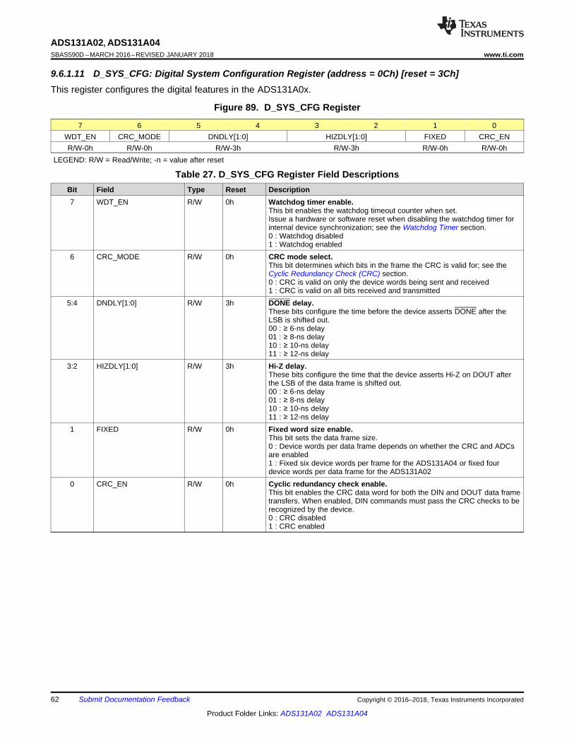
62
ADS131A02, ADS131A04SBAS590D –MARCH 2016–REVISED JANUARY 2018 www.ti.com
Product Folder Links: ADS131A02 ADS131A04
Submit Documentation Feedback Copyright © 2016–2018, Texas Instruments Incorporated
9.6.1.11 D_SYS_CFG: Digital System Configuration Register (address = 0Ch) [reset = 3Ch]This register configures the digital features in the ADS131A0x.
Figure 89. D_SYS_CFG Register
7 6 5 4 3 2 1 0WDT_EN CRC_MODE DNDLY[1:0] HIZDLY[1:0] FIXED CRC_ENR/W-0h R/W-0h R/W-3h R/W-3h R/W-0h R/W-0h
LEGEND: R/W = Read/Write; -n = value after reset
Table 27. D_SYS_CFG Register Field DescriptionsBit Field Type Reset Description7 WDT_EN R/W 0h Watchdog timer enable.
This bit enables the watchdog timeout counter when set.Issue a hardware or software reset when disabling the watchdog timer forinternal device synchronization; see the Watchdog Timer section.0 : Watchdog disabled1 : Watchdog enabled
6 CRC_MODE R/W 0h CRC mode select.This bit determines which bits in the frame the CRC is valid for; see theCyclic Redundancy Check (CRC) section.0 : CRC is valid on only the device words being sent and received1 : CRC is valid on all bits received and transmitted
5:4 DNDLY[1:0] R/W 3h DONE delay.These bits configure the time before the device asserts DONE after theLSB is shifted out.00 : ≥ 6-ns delay01 : ≥ 8-ns delay10 : ≥ 10-ns delay11 : ≥ 12-ns delay
3:2 HIZDLY[1:0] R/W 3h Hi-Z delay.These bits configure the time that the device asserts Hi-Z on DOUT afterthe LSB of the data frame is shifted out.00 : ≥ 6-ns delay01 : ≥ 8-ns delay10 : ≥ 10-ns delay11 : ≥ 12-ns delay
1 FIXED R/W 0h Fixed word size enable.This bit sets the data frame size.0 : Device words per data frame depends on whether the CRC and ADCsare enabled1 : Fixed six device words per frame for the ADS131A04 or fixed fourdevice words per data frame for the ADS131A02
0 CRC_EN R/W 0h Cyclic redundancy check enable.This bit enables the CRC data word for both the DIN and DOUT data frametransfers. When enabled, DIN commands must pass the CRC checks to berecognized by the device.0 : CRC disabled1 : CRC enabled
63
ADS131A02, ADS131A04www.ti.com SBAS590D –MARCH 2016–REVISED JANUARY 2018
Product Folder Links: ADS131A02 ADS131A04
Submit Documentation FeedbackCopyright © 2016–2018, Texas Instruments Incorporated
9.6.1.12 CLK1: Clock Configuration 1 Register (address = 0Dh) [reset = 08h]This register configures the ADC clocking and sets the internal clock dividers.
Figure 90. CLK1 Register
7 6 5 4 3 2 1 0CLKSRC 0 0 0 CLK_DIV[2:0] 0R/W-0h R/W-0h R/W-0h R/W-0h R/W-4h R/W-0h
LEGEND: R/W = Read/Write; -n = value after reset
Table 28. CLK1 Register Field DescriptionsBit Field Type Reset Description7 CLKSRC R/W 0h ADC clock source.
This bit selects the source for ICLK; see the Clock section for moreinformation on ADC clocking.0 : XTAL1/CLKIN pin or XTAL1/CLKIN and XTAL2 pins1 : SCLK pin
6:4 Reserved R/W 0h Reserved.Always write 0h.
3:1 CLK_DIV[2:0] R/W 4h CLKIN divider ratio.These bits set the CLKIN divider ratio to generate the internal fICLKfrequency. ICLK is used as the fSCLK output when the ADC is operating insynchronous master mode.000 : Reserved001 : fICLK = fCLKIN / 2010 : fICLK = fCLKIN / 4011 : fICLK = fCLKIN / 6100 : fICLK = fCLKIN / 8101 : fICLK = fCLKIN / 10110 : fICLK = fCLKIN / 12111 : fICLK = fCLKIN / 14
0 Reserved R/W 0h Reserved.Always write 0.

64
ADS131A02, ADS131A04SBAS590D –MARCH 2016–REVISED JANUARY 2018 www.ti.com
Product Folder Links: ADS131A02 ADS131A04
Submit Documentation Feedback Copyright © 2016–2018, Texas Instruments Incorporated
9.6.1.13 CLK2: Clock Configuration 2 Register (address = 0Eh) [reset = 86h]This register configures the ADC modulator clock and oversampling ratio for the converter.
Figure 91. CLK2 Register
7 6 5 4 3 2 1 0ICLK_DIV[2:0] 0 OSR[3:0]
R/W-4h R/W-0h R/W-6hLEGEND: R/W = Read/Write; -n = value after reset
Table 29. CLK2 Register Field DescriptionsBit Field Type Reset Description7:5 ICLK_DIV[2:0] R/W 4h ICLK divider ratio.
These bits set the divider ratio to generate the ADC modulator clock, fMOD,from the fICLK signal.000 : Reserved001 : fMOD = fICLK / 2010 : fMOD = fICLK / 4011 : fMOD = fICLK / 6100 : fMOD = fICLK / 8101 : fMOD = fICLK / 10110 : fMOD = fICLK / 12111 : fMOD = fICLK / 14
4 Reserved R/W 0h Reserved.Always write 0h.
3:0 OSR[3:0] R/W 6h Oversampling ratio.These bits set the OSR to create the ADC output data rate, fDATA; seeTable 30 for more details.0000 : fDATA = fMOD / 40960001 : fDATA = fMOD / 20480010 : fDATA = fMOD / 10240011 : fDATA = fMOD / 8000100 : fDATA = fMOD / 7680101 : fDATA = fMOD / 5120110 : fDATA = fMOD / 4000111 : fDATA = fMOD / 3841000 : fDATA = fMOD / 2561001 : fDATA = fMOD / 2001010 : fDATA = fMOD / 1921011 : fDATA = fMOD / 1281100 : fDATA = fMOD / 961101 : fDATA = fMOD / 641110 : fDATA = fMOD / 481111 : fDATA = fMOD / 32

65
ADS131A02, ADS131A04www.ti.com SBAS590D –MARCH 2016–REVISED JANUARY 2018
Product Folder Links: ADS131A02 ADS131A04
Submit Documentation FeedbackCopyright © 2016–2018, Texas Instruments Incorporated
Table 30. Data Rate Settings
OSR[3:0] OSR fDATA AT 2.048-MHz fMOD(kHz)
fDATA AT 4.096-MHz fMOD(kHz)
fDATA AT 4-MHz fMOD(kHz)
0000 4096 0.500 1.000 0.9770001 2048 1.000 2.000 1.9530010 1024 2.000 4.000 3.9060011 800 2.560 5.120 5.0000100 768 2.667 5.333 5.2080101 512 4.000 8.000 7.8130110 400 5.120 10.240 10.0000111 384 5.333 10.667 10.4171000 256 8.000 16.000 15.6251001 200 10.240 20.480 20.0001010 192 10.667 21.333 20.8331011 128 16.000 32.000 31.2501100 96 21.333 42.667 41.6671101 64 32.000 64.000 62.5001110 48 42.667 85.333 83.3331111 32 64.000 128.000 125.000
9.6.1.14 ADC_ENA: ADC Channel Enable Register (address = 0Fh) [reset = 00h]This register controls the enabling of ADC channels.
Figure 92. ADC_ENA Register
7 6 5 4 3 2 1 00 0 0 0 ENA[3:0]
R/W-0h R/W-0h R/W-0h R/W-0h R/W-0hLEGEND: R/W = Read/Write; -n = value after reset
Table 31. ADC_ENA Register Field DescriptionsBit Field Type Reset Description7:4 Reserved R/W 0h Reserved.
Always write 0h.3:0 ENA[3:0] R/W 0h Enable ADC channels.
These bits power-up or power-down the ADC channels. This setting isglobal for all channels.0000 : All ADC channels powered down1111 : All ADC channels powered upAll other settings: Do not use
66
ADS131A02, ADS131A04SBAS590D –MARCH 2016–REVISED JANUARY 2018 www.ti.com
Product Folder Links: ADS131A02 ADS131A04
Submit Documentation Feedback Copyright © 2016–2018, Texas Instruments Incorporated
9.6.1.15 Reserved Register (address = 10h) [reset = 00h]This register is reserved for future use.
Figure 93. Reserved Register
7 6 5 4 3 2 1 00 0 0 0 0 0 0 0
R/W-0h R/W-0h R/W-0h R/W-0h R/W-0h R/W-0h R/W-0h R/W-0hLEGEND: R = Read only; -n = value after reset
Table 32. Reserved Register Field DescriptionsBit Field Type Reset Description7:0 Reserved R/W 00h Reserved.
Always write 00h.
9.6.2 ADCx: ADC Channel Digital Gain Configuration Registers (address = 11h to 14h) [reset = 00h]These registers control the digital gain setting for the individual ADC channel (x denotes the ADC channel).For the ADS131A02, these registers are reserved.
Figure 94. ADCx Register
7 6 5 4 3 2 1 00 0 0 0 0 GAINx_[2:0]
R/W-0h R/W-0h R/W-0h R/W-0h R/W-0h R/W-0hLEGEND: R/W = Read/Write; -n = value after reset
Table 33. ADCx Registers Field DescriptionsBit Field Type Reset Description7:3 Reserved R/W 00h Reserved.
Always write 00h.2:0 GAINx_[2:0] R/W 0h Gain control (digital scaling).
These bits determine the digital gain of the ADC output.000 : Gain = 1001 : Gain = 2010 : Gain = 4011 : Gain = 8100 : Gain = 16101, 110, 111 : Reserved

Device
Phase APhase B
2.5 V
-2.5 V
AVDD
AVSS
AIN1P
AIN1N
AIN2P
AIN2N
R1
R2
R3
RFILT
RFILT
CFILT
CFILT
RFILT
CFILT
R1R2
CT
67
ADS131A02, ADS131A04www.ti.com SBAS590D –MARCH 2016–REVISED JANUARY 2018
Product Folder Links: ADS131A02 ADS131A04
Submit Documentation FeedbackCopyright © 2016–2018, Texas Instruments Incorporated
10 Application and Implementation
NOTEInformation in the following applications sections is not part of the TI componentspecification, and TI does not warrant its accuracy or completeness. TI’s customers areresponsible for determining suitability of components for their purposes. Customers shouldvalidate and test their design implementation to confirm system functionality.
10.1 Application Information
10.1.1 Unused Inputs and OutputsTo minimize leakage currents on the analog inputs, leave any unused analog inputs floating or connected toAVSS. For the ADS131A02, the NC pins (pins 5-8) can be left floating or tied directly to AVSS.
Pin 24 is a digital output unconnected (NC) pin. Leave pin 24 floating or tied to GND through a 10-kΩ pulldownresistor.
Do not float unused digital inputs because excessive power-supply leakage current can result. Tie all unuseddigital inputs to the appropriate levels, IOVDD or DGND, even when in power-down mode.
If the DONE or DRDY outputs are not used, leave these pins (pins 18 and 19, respectively) unconnected or tiethese pins to IOVDD using a weak pullup resistor. Current consumed by the pullup resistor flows into the deviceand therefore increases power consumption.
10.1.2 Power Monitoring Specific ApplicationsEach channel of the ADS131A0x is identical, giving designers the flexibility to sense voltage or current with anychannel. Simultaneous sampling allows the application to calculate instantaneous power for any simultaneousvoltage and current measurement. Figure 95 shows an example system that measures voltage and currentsimultaneously.
Figure 95. Example Power-Monitoring System
68
ADS131A02, ADS131A04SBAS590D –MARCH 2016–REVISED JANUARY 2018 www.ti.com
Product Folder Links: ADS131A02 ADS131A04
Submit Documentation Feedback Copyright © 2016–2018, Texas Instruments Incorporated
Application Information (continued)In Figure 95, channel 1 is dedicated to measuring the voltage between phase A and phase B and channel 2 isdedicated to measuring the current on phase A.
The resistors R1 and R2 form a voltage divider that steps the line voltage down to within the measurement rangeof the ADC. R1 can be formed by multiple resistors in series to dissipate power across several components. Thisconfiguration is also valid if the voltage is measured with respect to neutral instead of between phases.
Channel 2 is dedicated to measuring current that flows on phase A. Resistor R3 serves as a burden resistor thatshunts the current flowing across the secondary coil of the current transformer (CT). Current can also bemeasured using a Rogowski coil and an analog integrator or by performing integration digitally after aconversion.
The RC filters formed by RFILT and CFILT serve as antialiasing filters for the converter. If an application requires asteeper filter roll-off, a second-order RC filter can be used.
10.1.3 Multiple Device ConfigurationThe ADS131A0x allows the designer to add channels to the system by placing an additional device on the SPIbus. The first device in the chain of devices can be configured using any of the interface modes. All subsequentdevices must be configured in synchronous slave mode. In all cases, however, the chain of ADS131A0x devicesappear to the host as a single device with extra channels with the exception that each device sends individualstatus and data integrity words. In this manner, no additional pins on the host are required for more devices onthe chain. There are no special provisions that must be made in the interface except for extending the frame tothe appropriate length.
10.1.3.1 First Device Configured in Asynchronous Interrupt ModeFigure 96 illustrates a multiple device configuration where the first device is configured in asynchronous interruptmode as indicated by the state of the M0 pin. The second ADS131A0x device and any additional devices areconfigured in synchronous slave mode. The DONE pin of each device connects to the CS of the subsequentdevice. In each case, after a device shifts out all of its data, the device deasserts DONE, selecting thesubsequent device for communication. The DOUT of a device whose contents are already shifted out assumes ahigh-impedance state, allowing the DOUT pins of all devices to be tied together. To send commands to specificdevices, send the respective command of the device when that device is selected for communication. The DRDYoutput of the first device serves as the DRDY input to all other devices to synchronize conversions. Figure 97illustrates an example interface timing diagram for this configuration.
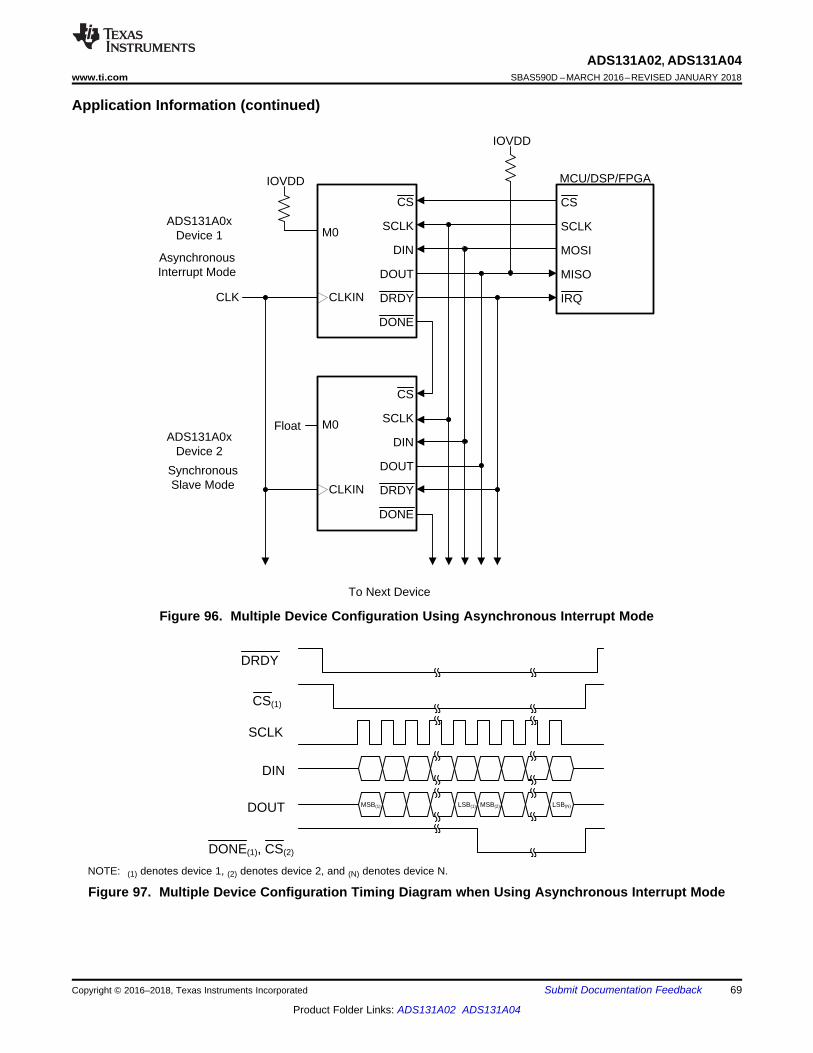
DRDY
CS(1)
SCLK
DOUT
DONE(1), CS(2)
MSB(1) LSB(1) MSB(2) LSB(N)
DIN
CS
SCLK
DIN
DOUT
DRDY
DONE
M0
CLKIN
IOVDD
CLK
CS
SCLK
MOSI
MISO
IRQ
CS
SCLK
DIN
DOUT
DRDY
DONE
M0
CLKIN
To Next Device
ADS131A0x Device 1
MCU/DSP/FPGA
ADS131A0x Device 2
Asynchronous Interrupt Mode
Synchronous Slave Mode
Float
IOVDD
69
ADS131A02, ADS131A04www.ti.com SBAS590D –MARCH 2016–REVISED JANUARY 2018
Product Folder Links: ADS131A02 ADS131A04
Submit Documentation FeedbackCopyright © 2016–2018, Texas Instruments Incorporated
Application Information (continued)
Figure 96. Multiple Device Configuration Using Asynchronous Interrupt Mode
NOTE: (1) denotes device 1, (2) denotes device 2, and (N) denotes device N.
Figure 97. Multiple Device Configuration Timing Diagram when Using Asynchronous Interrupt Mode

70
ADS131A02, ADS131A04SBAS590D –MARCH 2016–REVISED JANUARY 2018 www.ti.com
Product Folder Links: ADS131A02 ADS131A04
Submit Documentation Feedback Copyright © 2016–2018, Texas Instruments Incorporated
Application Information (continued)10.1.3.2 First Device Configured in Synchronous Master ModeFigure 98 shows a multiple device configuration where the first device is configured in synchronous master modeas indicated by the state of the M0 pin. The second ADS131A0x device and any additional devices areconfigured in synchronous slave mode. The DONE pin of each device connects to the CS pin of the subsequentdevice. In each case, after a device shifts out all of its data, the device deasserts DONE, selecting thesubsequent device for communication. Tie the DONE pin of the last device to the CS pin of the first device toallow for an immediate second read back of conversion data in the case a data integrity test failed. The DOUT ofa device whose contents are already shifted out assumes a high-impedance state, allowing the DOUT pins of alldevices to be tied together. To send commands to specific devices, send the respective command of the devicewhen that device is selected for communication. The DRDY output of the first device serves as the DRDY inputto all other devices to synchronize conversions. DRDY also serves as the chip-select or frame sync signal for thehost. SCLK is free running with the same frequency as ICLK in this configuration.Figure 99 illustrates an exampleinterface timing diagram for this configuration.

CS
SCLK
DIN
DOUT
DRDY
DONE
M0
CLKINCLKCS, FSYNC
SCLK
MISO
MOSI
CS
SCLK
DIN
DOUT
DRDY
DONE
M0
CLKIN
ADS131A0x Device 1
MCU/DSP/FPGA
ADS131A0x Device 2
Synchronous Master Mode
Synchronous Slave Mode
CS
SCLK
DIN
DOUT
DRDY
DONE
M0
CLKIN
ADS131A0x Device N
Synchronous Slave Mode
Devices 3 through N-1
Float
Float
IOVDD
71
ADS131A02, ADS131A04www.ti.com SBAS590D –MARCH 2016–REVISED JANUARY 2018
Product Folder Links: ADS131A02 ADS131A04
Submit Documentation FeedbackCopyright © 2016–2018, Texas Instruments Incorporated
Application Information (continued)
Figure 98. Multiple Device Configuration Using Synchronous Master Mode
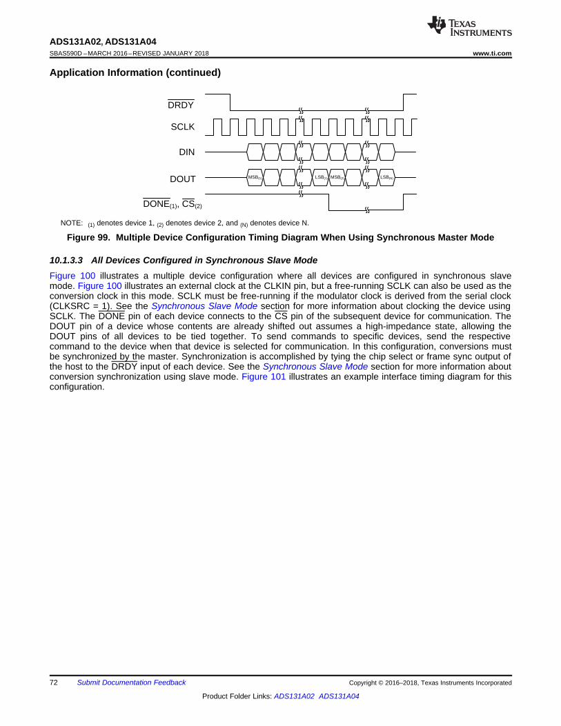
DRDY
SCLK
DOUT
DONE(1), CS(2)
MSB(1) LSB(1) MSB(2) LSB(N)
DIN
72
ADS131A02, ADS131A04SBAS590D –MARCH 2016–REVISED JANUARY 2018 www.ti.com
Product Folder Links: ADS131A02 ADS131A04
Submit Documentation Feedback Copyright © 2016–2018, Texas Instruments Incorporated
Application Information (continued)
NOTE: (1) denotes device 1, (2) denotes device 2, and (N) denotes device N.
Figure 99. Multiple Device Configuration Timing Diagram When Using Synchronous Master Mode
10.1.3.3 All Devices Configured in Synchronous Slave ModeFigure 100 illustrates a multiple device configuration where all devices are configured in synchronous slavemode. Figure 100 illustrates an external clock at the CLKIN pin, but a free-running SCLK can also be used as theconversion clock in this mode. SCLK must be free-running if the modulator clock is derived from the serial clock(CLKSRC = 1). See the Synchronous Slave Mode section for more information about clocking the device usingSCLK. The DONE pin of each device connects to the CS pin of the subsequent device for communication. TheDOUT pin of a device whose contents are already shifted out assumes a high-impedance state, allowing theDOUT pins of all devices to be tied together. To send commands to specific devices, send the respectivecommand to the device when that device is selected for communication. In this configuration, conversions mustbe synchronized by the master. Synchronization is accomplished by tying the chip select or frame sync output ofthe host to the DRDY input of each device. See the Synchronous Slave Mode section for more information aboutconversion synchronization using slave mode. Figure 101 illustrates an example interface timing diagram for thisconfiguration.
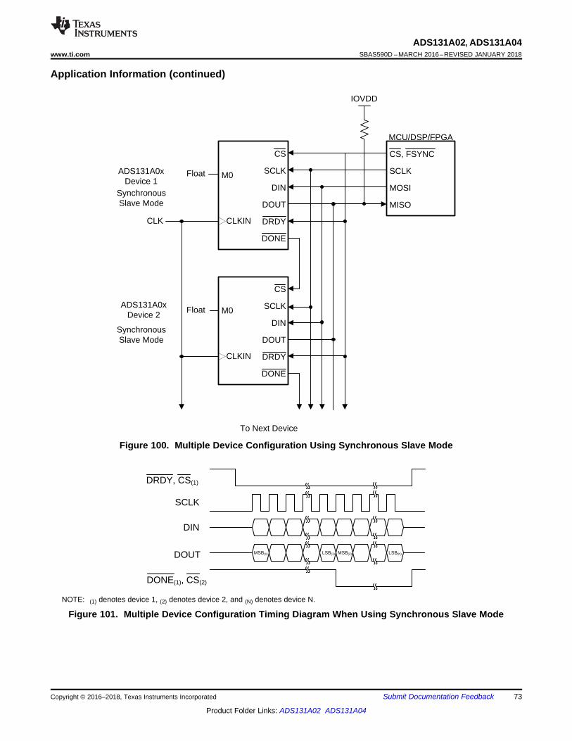
DRDY, CS(1)
SCLK
DOUT
DONE(1), CS(2)
MSB(1) LSB(1) MSB(2) LSB(N)
DIN
CS
SCLK
DIN
DOUT
DRDY
DONE
M0
CLKINCLK
CS, FSYNC
SCLK
MOSI
MISO
CS
SCLK
DIN
DOUT
DRDY
DONE
M0
CLKIN
To Next Device
ADS131A0x Device 1
MCU/DSP/FPGA
ADS131A0x Device 2
Synchronous Slave Mode
Synchronous Slave Mode
Float
Float
IOVDD
73
ADS131A02, ADS131A04www.ti.com SBAS590D –MARCH 2016–REVISED JANUARY 2018
Product Folder Links: ADS131A02 ADS131A04
Submit Documentation FeedbackCopyright © 2016–2018, Texas Instruments Incorporated
Application Information (continued)
Figure 100. Multiple Device Configuration Using Synchronous Slave Mode
NOTE: (1) denotes device 1, (2) denotes device 2, and (N) denotes device N.
Figure 101. Multiple Device Configuration Timing Diagram When Using Synchronous Slave Mode

ADS131A04
AVDD
INxN
2.5 V
INxP
INxN
-2.5 V
AVSS
C1
C1
R1 R1R1
R2
R3
R3
R3
R3
R4
R4
INxPLine
Neutral
Line Current IN
Line Current OUT
2000:1
74
ADS131A02, ADS131A04SBAS590D –MARCH 2016–REVISED JANUARY 2018 www.ti.com
Product Folder Links: ADS131A02 ADS131A04
Submit Documentation Feedback Copyright © 2016–2018, Texas Instruments Incorporated
10.2 Typical ApplicationFigure 102 shows an ADS131A0x device used as part of a power-metering application. The ADS131A0x deviceis ideal because this device allows for simultaneous sampling of voltage and current. The upper channel is usedto measure voltage, accomplished by stepping down the line voltage with a voltage divider. The lower channelmeasures current directly from the line by measuring voltage across the burden resistors R4.
Figure 102. Typical Power Metering Connections
10.2.1 Design Requirements
Table 34. Power Metering Design RequirementsDESIGN PARAMETER VALUE
Voltage input 230 VRMS at 50 HzCurrent input range 0.05 ARMS to 100 ARMS
Active power measurement error < 0.2%
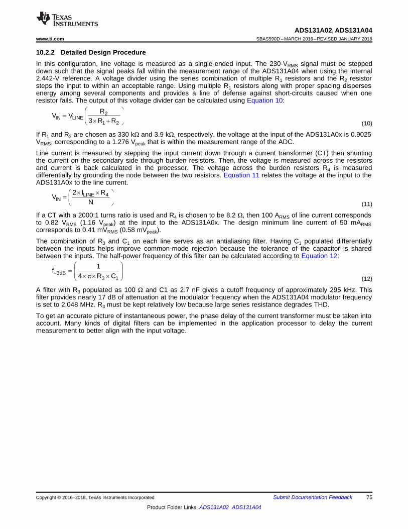
3dB3 1
1f
4 R C
§ · ¨ ¸
u Su u© ¹
LINE 4IN
2 I RV
Nu u§ ·
¨ ¸© ¹
2IN LINE
1 2
RV V
3 R R
§ · ¨ ¸
u © ¹
75
ADS131A02, ADS131A04www.ti.com SBAS590D –MARCH 2016–REVISED JANUARY 2018
Product Folder Links: ADS131A02 ADS131A04
Submit Documentation FeedbackCopyright © 2016–2018, Texas Instruments Incorporated
10.2.2 Detailed Design ProcedureIn this configuration, line voltage is measured as a single-ended input. The 230-VRMS signal must be steppeddown such that the signal peaks fall within the measurement range of the ADS131A04 when using the internal2.442-V reference. A voltage divider using the series combination of multiple R1 resistors and the R2 resistorsteps the input to within an acceptable range. Using multiple R1 resistors along with proper spacing dispersesenergy among several components and provides a line of defense against short-circuits caused when oneresistor fails. The output of this voltage divider can be calculated using Equation 10:
(10)
If R1 and R2 are chosen as 330 kΩ and 3.9 kΩ, respectively, the voltage at the input of the ADS131A0x is 0.9025VRMS, corresponding to a 1.276 Vpeak that is within the measurement range of the ADC.
Line current is measured by stepping the input current down through a current transformer (CT) then shuntingthe current on the secondary side through burden resistors. Then, the voltage is measured across the resistorsand current is back calculated in the processor. The voltage across the burden resistors R4 is measureddifferentially by grounding the node between the two resistors. Equation 11 relates the voltage at the input to theADS131A0x to the line current.
(11)
If a CT with a 2000:1 turns ratio is used and R4 is chosen to be 8.2 Ω, then 100 ARMS of line current correspondsto 0.82 VRMS (1.16 Vpeak) at the input to the ADS131A0x. The design minimum line current of 50 mARMScorresponds to 0.41 mVRMS (0.58 mVpeak).
The combination of R3 and C1 on each line serves as an antialiasing filter. Having C1 populated differentiallybetween the inputs helps improve common-mode rejection because the tolerance of the capacitor is sharedbetween the inputs. The half-power frequency of this filter can be calculated according to Equation 12:
(12)
A filter with R3 populated as 100 Ω and C1 as 2.7 nF gives a cutoff frequency of approximately 295 kHz. Thisfilter provides nearly 17 dB of attenuation at the modulator frequency when the ADS131A04 modulator frequencyis set to 2.048 MHz. R3 must be kept relatively low because large series resistance degrades THD.
To get an accurate picture of instantaneous power, the phase delay of the current transformer must be taken intoaccount. Many kinds of digital filters can be implemented in the application processor to delay the currentmeasurement to better align with the input voltage.

Current Magnitude (A)
Err
or (
%)
0 10 20 30 40 50 60 70 80 90 100-0.5
-0.4
-0.3
-0.2
-0.1
0
0.1
0.2
0.3
0.4
0.5
D007
Power FactorUnity0.5 Lead0.5 Lag
76
ADS131A02, ADS131A04SBAS590D –MARCH 2016–REVISED JANUARY 2018 www.ti.com
Product Folder Links: ADS131A02 ADS131A04
Submit Documentation Feedback Copyright © 2016–2018, Texas Instruments Incorporated
10.2.3 Application CurveFigure 103 shows the active power measurement accuracy for the ADS131A0x across varying currents. Datawas taken for a 0.5 lead, 0.5 lag, and unity power factors. For this test, the external 16.384-MHz crystalfrequency was divided to give a modulator frequency of 2.048 MHz. Finally, an OSR of 256 was chosen to givethe ADS131A04 an output data rate of 8 kSPS.
Figure 103. Active Power Measurement Error
10.3 Do's and Don'ts• Do partition the analog, digital, and power-supply circuitry into separate sections on the printed circuit board
(PCB).• Do use a single ground plane for analog and digital grounds.• Do place the analog components close to the ADC pins using short, direct connections.• Do keep the SCLK pin free of glitches and noise.• Do verify that the analog input voltages are within the specified voltage range under all input conditions.• Do tie unused analog input pins to GND.• Do provide current limiting to the analog inputs in case overvoltage faults occur.• Do use a low-dropout (LDO) regulator to reduce ripple voltage generated by switch-mode power supplies.
This reduction is especially true for AVDD where the supply noise can affect performance.• Do keep the input series resistance low to maximize THD performance.• Do not cross analog and digital signals.• Do not allow the analog power supply voltages (AVDD – AVSS) to exceed 3.6 V under any conditions,
including during power-up and power-down when the negative charge pump is enabled.• Do not allow the analog power supply voltages (AVDD – AVSS) to exceed 6 V under any conditions,
including during power-up and power-down when the negative charge pump is disabled.• Do not allow the digital supply voltage to exceed 3.9 V under any conditions, including during power-up and
power-down.
Figure 104 and Figure 105 illustrate correct and incorrect ADC circuit connections.
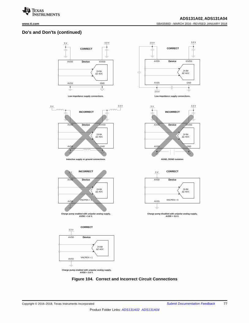
24-Bitû ADC
DeviceAVDD
AVSS
IOVDD
GND
3.3 V5 V
Low-impedance supply connections.
24-Bitû ADC
DeviceAVDD
AVSS
IOVDD
GND
3.3 V2.5 V
Low-impedance supply connections.
-2.5 V
24-Bitû ADC
DeviceAVDD
AVSS
IOVDD
GND
Inductive supply or ground connections.
5 V 3.3 V
24-Bitû ADC
DeviceAVDD
AVSS
IOVDD
GND
3.3 V5 V
AGND, DGND isolation.
24-Bitû ADC
DeviceAVDD
AVSS
5 V
VNCPEN = 1
Charge pump enabled with unipolar analog supply, AVDD > 3.6 V.
24-Bitû ADC
DeviceAVDD
AVSS
5 V
VNCPEN = 0
Charge pump disabled with unipolar analog supply, AVDD > 3.6 V.
CORRECT
CORRECTCORRECT
INCORRECT
INCORRECTINCORRECT
24-Bitû ADC
DeviceAVDD
AVSS
3.3 V
VNCPEN = 1
Charge pump enabled with unipolar analog supply, AVDD < 3.6 V.
CORRECT
77
ADS131A02, ADS131A04www.ti.com SBAS590D –MARCH 2016–REVISED JANUARY 2018
Product Folder Links: ADS131A02 ADS131A04
Submit Documentation FeedbackCopyright © 2016–2018, Texas Instruments Incorporated
Do's and Don'ts (continued)
Figure 104. Correct and Incorrect Circuit Connections

24-Bitû ADC
DeviceAVDD
AVSS
2.5 V
VNCPEN = 1
Charge pump is enabled with a bipolar analog supply.
-2.5 V
24-Bitû ADC
DeviceAVDD
AVSS
2.5 V
VNCPEN = 0
Charge pump is disabled with a bipolar analog supply.
-2.5 V
24-Bitû ADC
DeviceAVDD
AVSS
3.3 VCORRECT
VNCPEN = 1
Input swings below ground, charge pump is enabled.
+
±
AIN1P
AIN1N
-1 V
24-Bitû ADC
DeviceAVDD
AVSS
3.3 VINCORRECT
VNCPEN = 0
Input swings below ground, charge pump is disabled.
AINxP
AINxN
CORRECTINCORRECT
+
±
-1 V
78
ADS131A02, ADS131A04SBAS590D –MARCH 2016–REVISED JANUARY 2018 www.ti.com
Product Folder Links: ADS131A02 ADS131A04
Submit Documentation Feedback Copyright © 2016–2018, Texas Instruments Incorporated
Do's and Don'ts (continued)
Figure 105. Correct and Incorrect Circuit Connections, Continued
10.4 Initialization Set UpFigure 106 illustrates a general procedure to configure the ADS131A0x to collect data.

Power Off
SETRESET = 1
// RESET can come up with Power Supply
Receive Command Status Response
Write another register?
Capture Data
// Analog and Digital supply can come up together
// Use the WREG or WREGS commands
// Send WAKEUP command 0x0033// Start conversions
// Use DRDY indicator to indicate new data is available
// Verify registers are written successfully// Device Data Frame or Data Rate may change if coresponding register is changed
Set M0 mode pin
Power upAnalog + Digital Supply
Unlock Device
Wait
Y
N
Receive READY Word?
Write Registers
Y
Enable ADCs // Write 0Fh to the ADC_ENA register to enable ADCs
N
// Configure Int/Ext reference, CLK dividers, OSR, comparator threshold, negative charge pump, and power mode setting
// Send UNLOCK command 0x0655// Receive Command Status Response 0x0655
// Monitor serial output for 0xFF02 (ADS131A02) or 0xFF04 (ADS131A04)
// Send LOCK command 0x0555
// Pull up, pull down or float the M0 pin
Wakeup Device
Configure Device
Lock Registers
79
ADS131A02, ADS131A04www.ti.com SBAS590D –MARCH 2016–REVISED JANUARY 2018
Product Folder Links: ADS131A02 ADS131A04
Submit Documentation FeedbackCopyright © 2016–2018, Texas Instruments Incorporated
Initialization Set Up (continued)
Figure 106. ADS131A0x Configuration Sequence

80
ADS131A02, ADS131A04SBAS590D –MARCH 2016–REVISED JANUARY 2018 www.ti.com
Product Folder Links: ADS131A02 ADS131A04
Submit Documentation Feedback Copyright © 2016–2018, Texas Instruments Incorporated
11 Power Supply RecommendationsThe device requires two power supplies: analog (AVDD, AVSS) and digital (IOVDD, GND). The analog powersupply can be bipolar (for example, AVDD = 2.5 V, AVSS = –2.5 V), unipolar (for example, AVDD = 5 V, AVSS =0 V), or unipolar using the negative charge pump (for example, AVDD = 3.3 V, AVSS = VNCP), and isindependent of the digital power supply. The digital supply range sets the digital I/O levels.
11.1 Negative Charge PumpAn optional negative charge pump is available to power AVSS with an operating voltage of –1.95 V. Enabling thenegative charge pump allows for input signals below analog ground when using a unipolar analog supply (forexample, AVDD = 3.3 V, AVSS = 0 V). The VNCPEN bit in the A_SYS_CFG register must be set high by theuser to enable the negative charge pump. The VNCP pin outputs the nominal –1.95-V negative charge pumpoutput and requires a capacitor to AVSS in the range of 220 pF to 470 pF. The charge pump operates at aswitching frequency of 2fMOD. The minimum ADC absolute input voltage range is –1.5 V with the negative chargepump enabled. The maximum analog supply limit (AVDD – AVSS) is restricted to 3.6 V maximum. Exceeding thislimit can permanently damage the device.
The negative charge pump is internally activated when the VNCPEN bit is set to 1 and the device is in wake-upmode with all ADC channels enabled (ADC_ENA = 0Fh).
Connect VNCP directly to AVSS when not using the negative charge pump.
11.2 Internal Digital LDOThe ADS131A0x digital core voltage operates from 1.8 V, created from an internal LDO from IOVDD. The CAPpin outputs the LDO voltage created from the IOVDD supply and requires an external bypass capacitor. Whenoperating from VIOVDD > 2 V, place a 1-µF capacitor on the CAP pin to GND. If VIOVDD ≤ 2 V, tie the CAP pindirectly to the IOVDD pin and decouple both pins using a 1-µF capacitor to GND.
11.3 Power-Supply SequencingThe power supplies can be sequenced in any order but the analog or digital inputs must never exceed therespective analog or digital power-supply voltage limits.

3.3 V 3.3 V
TI Device
AVDD
VNCPAVSS GND
IOVDD
REFP
REFN
CAP1RESV
1 PF 1 PF
1 PF
REFEXT
1 PF
1 PF
270 nF
CAP2
10 pF
Copyright © 2017, Texas Instruments Incorporated
2.5 V 3.3 V
TI Device
AVDD
VNCPAVSS GND
IOVDD
REFP
REFN
CAP1RESV
1 PF
1 PF
REFEXT
1 PF
1 PF
-2.5 V
-2.5 V
-2.5 V
CAP2
10 pF
Copyright © 2017, Texas Instruments Incorporated
1 PF
-2.5 V
5 V
TI Device
AVDD
VNCPAVSS GND
IOVDD
REFP
REFN
CAP1RESV
1 PF
1 PF
REFEXT
1 PF
1 PF
CAP2
10 pF
Copyright © 2017, Texas Instruments Incorporated
3.3 V
1 PF
81
ADS131A02, ADS131A04www.ti.com SBAS590D –MARCH 2016–REVISED JANUARY 2018
Product Folder Links: ADS131A02 ADS131A04
Submit Documentation FeedbackCopyright © 2016–2018, Texas Instruments Incorporated
11.4 Power-Supply DecouplingGood power-supply decoupling is important to achieve optimum performance. AVDD, AVSS (when using abipolar supply), and IOVDD must be decoupled with at least a 1-µF capacitor, as shown in Figure 107,Figure 108, and Figure 109. A 270-nF capacitor is required on the VNCP pin when using the negative chargepump. Place the bypass capacitors as close to the power-supply pins of the device as possible with low-impedance connections. Using multi-layer ceramic chip capacitors (MLCCs) that offer low equivalent seriesresistance (ESR) and inductance (ESL) characteristics are recommended for power-supply decoupling purposes.For very sensitive systems, or for systems in harsh noise environments, avoiding the use of vias for connectingthe capacitors to the device pins can offer superior noise immunity. The use of multiple vias in parallel lowers theoverall inductance and is beneficial for connections to ground planes. The analog and digital ground arerecommended to be connected together as close to the device as possible.
Figure 107. Bipolar Analog Power SupplyFigure 108. Unipolar Analog Power Supply
Figure 109. Unipolar Analog Power Supply with Negative Charge Pump Enabled

Device Microcontroller
Signal
Conditioning
(RC Filters
and
Amplifiers)
Supply
Generation
Connector
or Antenna
Ground Fill orGround Plane
Op
tio
na
l: S
plit
Gro
und
Cu
tGround Fill orGround Plane
Op
tio
na
l: S
plit
Gro
un
d C
ut
InterfaceTransceiver
Ground Fill orGround Plane
Ground Fill orGround Plane
82
ADS131A02, ADS131A04SBAS590D –MARCH 2016–REVISED JANUARY 2018 www.ti.com
Product Folder Links: ADS131A02 ADS131A04
Submit Documentation Feedback Copyright © 2016–2018, Texas Instruments Incorporated
12 Layout
12.1 Layout GuidelinesUse a low-impedance connection for ground so that return currents flow undisturbed back to the respectivesources. For best performance, dedicate an entire PCB layer to a ground plane and do not route any other signaltraces on this layer. Keep connections to the ground plane as short and direct as possible. When using vias toconnect to the ground layer, use multiple vias in parallel to reduce impedance to ground. Figure 110 shows theproper component placement for the system.
A mixed-signal layout sometimes incorporates separate analog and digital ground planes that are tied together atone location; however, separating the ground planes is not necessary when analog, digital, and power-supplycomponents are properly placed. Proper placement of components partitions the analog, digital, and power-supply circuitry into different PCB regions to prevent digital return currents from coupling into sensitive analogcircuitry. If ground plane separation is necessary, then make the connection at the ADC. Connecting individualground planes at multiple locations creates ground loops, and is not recommended. A single ground plane for theanalog and digital grounds avoids ground loops.
Bypass the supply pins with a low-ESR ceramic capacitor. The placement of the bypass capacitors must be asclose as possible to the supply pins using short, direct traces. For optimum performance, the ground-sideconnections of the bypass capacitors must also be made with low-impedance connections. The supply currentflows through the bypass capacitor pin first and then to the supply pin to make the bypassing most effective (alsoknown as a Kelvin connection). If multiple ADCs are on the same PCB, use wide power-supply traces ordedicated power-supply planes to minimize the potential of crosstalk between ADCs.
If external filtering is used for the analog inputs, use C0G-type ceramic capacitors when possible. C0Gcapacitors have stable properties and low-noise characteristics. Ideally, route differential signals as pairs tominimize the loop area between the traces. Route digital circuit traces (such as clock signals) away from allanalog pins. Note that the internal reference output return shares the same pin as the AVSS power supply. Tominimize coupling between the power-supply trace and reference return trace, route the two traces separately;ideally, as a star connection at the AVSS pin.
Treat the AVSS pin as a sensitive analog signal and connect directly to the supply ground with proper shielding.Leakage currents between the PCB traces can exceed the input bias current of the ADS131A0x if shielding is notimplemented. Keep digital signals as far as possible from the analog input signals on the PCB.
The SCLK input of the serial interface must be free from noise and glitches when this device is configured in aslave mode. This configuration is especially true when SCLK is used as the master clock for this device. Evenwith relatively slow SCLK frequencies, short digital signal rise and fall times can cause excessive ringing andnoise. For best performance, keep the digital signal traces short, using termination resistors as needed, andmake sure all digital signals are routed directly above the ground plane with minimal use of vias.
Figure 110. System Component Placement

1: AIN1N
2: AIN1P
3: AIN2N
4: AIN2P
5: AIN3N
6: AIN3P
7: AIN4N
8: AIN4P
9: A
VD
D
10: A
VS
S
13: R
EF
N
11: V
NC
P
12: R
EF
P
14: R
EF
EX
T
15: I
OV
DD
16: R
ES
V
17: RESET
18: DONE
19: DRDY
20:DIN
21:DOUT
22: SCLK
23: CS
24: NC
25: X
TA
L1
26: X
TA
L2
27: G
ND
28: C
AP
29: I
OV
DD
30: M
0
31: M
1
32: M
2
+2.5 V
-2.5 V
+3.3 V
-2.5 V
-2.5 V
Device
+3.3 V Via to corresponding voltage plane or pour
Via to ground plane or pour
Inputs filtered with differential capacitors
Reference, CAP, and power supply decoupling capacitors
close to pins
Long digital input lines terminated with resistors to
prevent reflection
+3.3 V
83
ADS131A02, ADS131A04www.ti.com SBAS590D –MARCH 2016–REVISED JANUARY 2018
Product Folder Links: ADS131A02 ADS131A04
Submit Documentation FeedbackCopyright © 2016–2018, Texas Instruments Incorporated
12.2 Layout ExampleFigure 111 is an example layout of the ADS131A0x. This example shows the device supplied with a bipolarsupply, though the layout can be replicated for a unipolar case. In general, analog signals and planes arepartitioned to the left and digital signals and planes to the right.
Figure 111. ADS131A0x Layout Example

84
ADS131A02, ADS131A04SBAS590D –MARCH 2016–REVISED JANUARY 2018 www.ti.com
Product Folder Links: ADS131A02 ADS131A04
Submit Documentation Feedback Copyright © 2016–2018, Texas Instruments Incorporated
13 Device and Documentation Support
13.1 Documentation Support
13.1.1 Related DocumentationFor related documentation see the following:• REF50xx Low-Noise, Very Low Drift, Precision Voltage Reference (SBOS410)• THS4531A Ultra Low-Power, Rail-to-Rail Output, Fully Differential Amplifier (SLOS823)• REF60xx High-Precision Voltage Reference With Integrated ADC Drive Buffer (SBOS708)
13.2 Related LinksThe table below lists quick access links. Categories include technical documents, support and communityresources, tools and software, and quick access to order now.
Table 35. Related Links
PARTS PRODUCT FOLDER ORDER NOW TECHNICALDOCUMENTS
TOOLS &SOFTWARE
SUPPORT &COMMUNITY
ADS131A02 Click here Click here Click here Click here Click hereADS131A04 Click here Click here Click here Click here Click here
13.3 Receiving Notification of Documentation UpdatesTo receive notification of documentation updates, navigate to the device product folder on ti.com. In the upperright corner, click on Alert me to register and receive a weekly digest of any product information that haschanged. For change details, review the revision history included in any revised document.
13.4 Community ResourcesThe following links connect to TI community resources. Linked contents are provided "AS IS" by the respectivecontributors. They do not constitute TI specifications and do not necessarily reflect TI's views; see TI's Terms ofUse.
TI E2E™ Online Community TI's Engineer-to-Engineer (E2E) Community. Created to foster collaborationamong engineers. At e2e.ti.com, you can ask questions, share knowledge, explore ideas and helpsolve problems with fellow engineers.
Design Support TI's Design Support Quickly find helpful E2E forums along with design support tools andcontact information for technical support.
13.5 TrademarksE2E is a trademark of Texas Instruments.All other trademarks are the property of their respective owners.
13.6 Electrostatic Discharge CautionThis integrated circuit can be damaged by ESD. Texas Instruments recommends that all integrated circuits be handled withappropriate precautions. Failure to observe proper handling and installation procedures can cause damage.
ESD damage can range from subtle performance degradation to complete device failure. Precision integrated circuits may be moresusceptible to damage because very small parametric changes could cause the device not to meet its published specifications.
13.7 GlossarySLYZ022 — TI Glossary.
This glossary lists and explains terms, acronyms, and definitions.

85
ADS131A02, ADS131A04www.ti.com SBAS590D –MARCH 2016–REVISED JANUARY 2018
Product Folder Links: ADS131A02 ADS131A04
Submit Documentation FeedbackCopyright © 2016–2018, Texas Instruments Incorporated
14 Mechanical, Packaging, and Orderable InformationThe following pages include mechanical, packaging, and orderable information. This information is the mostcurrent data available for the designated devices. This data is subject to change without notice and revision ofthis document. For browser-based versions of this data sheet, refer to the left-hand navigation.
PACKAGE OPTION ADDENDUM
www.ti.com 14-Dec-2017
Addendum-Page 1
PACKAGING INFORMATION
Orderable Device Status(1)
Package Type PackageDrawing
Pins PackageQty
Eco Plan(2)
Lead/Ball Finish(6)
MSL Peak Temp(3)
Op Temp (°C) Device Marking(4/5)
Samples
ADS131A02IPBS ACTIVE TQFP PBS 32 250 Green (RoHS& no Sb/Br)
CU NIPDAU Level-2-260C-1 YEAR -40 to 125 131A02
ADS131A02IPBSR ACTIVE TQFP PBS 32 1000 Green (RoHS& no Sb/Br)
CU NIPDAU Level-2-260C-1 YEAR -40 to 125 131A02
ADS131A04IPBS ACTIVE TQFP PBS 32 250 Green (RoHS& no Sb/Br)
CU NIPDAU Level-2-260C-1 YEAR -40 to 125 131A04
ADS131A04IPBSR ACTIVE TQFP PBS 32 1000 Green (RoHS& no Sb/Br)
CU NIPDAU Level-2-260C-1 YEAR -40 to 125 131A04
(1) The marketing status values are defined as follows:ACTIVE: Product device recommended for new designs.LIFEBUY: TI has announced that the device will be discontinued, and a lifetime-buy period is in effect.NRND: Not recommended for new designs. Device is in production to support existing customers, but TI does not recommend using this part in a new design.PREVIEW: Device has been announced but is not in production. Samples may or may not be available.OBSOLETE: TI has discontinued the production of the device.
(2) RoHS: TI defines "RoHS" to mean semiconductor products that are compliant with the current EU RoHS requirements for all 10 RoHS substances, including the requirement that RoHS substancedo not exceed 0.1% by weight in homogeneous materials. Where designed to be soldered at high temperatures, "RoHS" products are suitable for use in specified lead-free processes. TI mayreference these types of products as "Pb-Free".RoHS Exempt: TI defines "RoHS Exempt" to mean products that contain lead but are compliant with EU RoHS pursuant to a specific EU RoHS exemption.Green: TI defines "Green" to mean the content of Chlorine (Cl) and Bromine (Br) based flame retardants meet JS709B low halogen requirements of <=1000ppm threshold. Antimony trioxide basedflame retardants must also meet the <=1000ppm threshold requirement.
(3) MSL, Peak Temp. - The Moisture Sensitivity Level rating according to the JEDEC industry standard classifications, and peak solder temperature.
(4) There may be additional marking, which relates to the logo, the lot trace code information, or the environmental category on the device.
(5) Multiple Device Markings will be inside parentheses. Only one Device Marking contained in parentheses and separated by a "~" will appear on a device. If a line is indented then it is a continuationof the previous line and the two combined represent the entire Device Marking for that device.
(6) Lead/Ball Finish - Orderable Devices may have multiple material finish options. Finish options are separated by a vertical ruled line. Lead/Ball Finish values may wrap to two lines if the finishvalue exceeds the maximum column width.
Important Information and Disclaimer:The information provided on this page represents TI's knowledge and belief as of the date that it is provided. TI bases its knowledge and belief on informationprovided by third parties, and makes no representation or warranty as to the accuracy of such information. Efforts are underway to better integrate information from third parties. TI has taken and

PACKAGE OPTION ADDENDUM
www.ti.com 14-Dec-2017
Addendum-Page 2
continues to take reasonable steps to provide representative and accurate information but may not have conducted destructive testing or chemical analysis on incoming materials and chemicals.TI and TI suppliers consider certain information to be proprietary, and thus CAS numbers and other limited information may not be available for release.
In no event shall TI's liability arising out of such information exceed the total purchase price of the TI part(s) at issue in this document sold by TI to Customer on an annual basis.

TAPE AND REEL INFORMATION
*All dimensions are nominal
Device PackageType
PackageDrawing
Pins SPQ ReelDiameter
(mm)
ReelWidth
W1 (mm)
A0(mm)
B0(mm)
K0(mm)
P1(mm)
W(mm)
Pin1Quadrant
ADS131A02IPBSR TQFP PBS 32 1000 330.0 16.4 7.2 7.2 1.5 12.0 16.0 Q2
ADS131A04IPBSR TQFP PBS 32 1000 330.0 16.4 7.2 7.2 1.5 12.0 16.0 Q2
PACKAGE MATERIALS INFORMATION
www.ti.com 14-Dec-2017
Pack Materials-Page 1

*All dimensions are nominal
Device Package Type Package Drawing Pins SPQ Length (mm) Width (mm) Height (mm)
ADS131A02IPBSR TQFP PBS 32 1000 367.0 367.0 38.0
ADS131A04IPBSR TQFP PBS 32 1000 367.0 367.0 38.0
PACKAGE MATERIALS INFORMATION
www.ti.com 14-Dec-2017
Pack Materials-Page 2


IMPORTANT NOTICE
Texas Instruments Incorporated (TI) reserves the right to make corrections, enhancements, improvements and other changes to itssemiconductor products and services per JESD46, latest issue, and to discontinue any product or service per JESD48, latest issue. Buyersshould obtain the latest relevant information before placing orders and should verify that such information is current and complete.TI’s published terms of sale for semiconductor products (http://www.ti.com/sc/docs/stdterms.htm) apply to the sale of packaged integratedcircuit products that TI has qualified and released to market. Additional terms may apply to the use or sale of other types of TI products andservices.Reproduction of significant portions of TI information in TI data sheets is permissible only if reproduction is without alteration and isaccompanied by all associated warranties, conditions, limitations, and notices. TI is not responsible or liable for such reproduceddocumentation. Information of third parties may be subject to additional restrictions. Resale of TI products or services with statementsdifferent from or beyond the parameters stated by TI for that product or service voids all express and any implied warranties for theassociated TI product or service and is an unfair and deceptive business practice. TI is not responsible or liable for any such statements.Buyers and others who are developing systems that incorporate TI products (collectively, “Designers”) understand and agree that Designersremain responsible for using their independent analysis, evaluation and judgment in designing their applications and that Designers havefull and exclusive responsibility to assure the safety of Designers' applications and compliance of their applications (and of all TI productsused in or for Designers’ applications) with all applicable regulations, laws and other applicable requirements. Designer represents that, withrespect to their applications, Designer has all the necessary expertise to create and implement safeguards that (1) anticipate dangerousconsequences of failures, (2) monitor failures and their consequences, and (3) lessen the likelihood of failures that might cause harm andtake appropriate actions. Designer agrees that prior to using or distributing any applications that include TI products, Designer willthoroughly test such applications and the functionality of such TI products as used in such applications.TI’s provision of technical, application or other design advice, quality characterization, reliability data or other services or information,including, but not limited to, reference designs and materials relating to evaluation modules, (collectively, “TI Resources”) are intended toassist designers who are developing applications that incorporate TI products; by downloading, accessing or using TI Resources in anyway, Designer (individually or, if Designer is acting on behalf of a company, Designer’s company) agrees to use any particular TI Resourcesolely for this purpose and subject to the terms of this Notice.TI’s provision of TI Resources does not expand or otherwise alter TI’s applicable published warranties or warranty disclaimers for TIproducts, and no additional obligations or liabilities arise from TI providing such TI Resources. TI reserves the right to make corrections,enhancements, improvements and other changes to its TI Resources. TI has not conducted any testing other than that specificallydescribed in the published documentation for a particular TI Resource.Designer is authorized to use, copy and modify any individual TI Resource only in connection with the development of applications thatinclude the TI product(s) identified in such TI Resource. NO OTHER LICENSE, EXPRESS OR IMPLIED, BY ESTOPPEL OR OTHERWISETO ANY OTHER TI INTELLECTUAL PROPERTY RIGHT, AND NO LICENSE TO ANY TECHNOLOGY OR INTELLECTUAL PROPERTYRIGHT OF TI OR ANY THIRD PARTY IS GRANTED HEREIN, including but not limited to any patent right, copyright, mask work right, orother intellectual property right relating to any combination, machine, or process in which TI products or services are used. Informationregarding or referencing third-party products or services does not constitute a license to use such products or services, or a warranty orendorsement thereof. Use of TI Resources may require a license from a third party under the patents or other intellectual property of thethird party, or a license from TI under the patents or other intellectual property of TI.TI RESOURCES ARE PROVIDED “AS IS” AND WITH ALL FAULTS. TI DISCLAIMS ALL OTHER WARRANTIES ORREPRESENTATIONS, EXPRESS OR IMPLIED, REGARDING RESOURCES OR USE THEREOF, INCLUDING BUT NOT LIMITED TOACCURACY OR COMPLETENESS, TITLE, ANY EPIDEMIC FAILURE WARRANTY AND ANY IMPLIED WARRANTIES OFMERCHANTABILITY, FITNESS FOR A PARTICULAR PURPOSE, AND NON-INFRINGEMENT OF ANY THIRD PARTY INTELLECTUALPROPERTY RIGHTS. TI SHALL NOT BE LIABLE FOR AND SHALL NOT DEFEND OR INDEMNIFY DESIGNER AGAINST ANY CLAIM,INCLUDING BUT NOT LIMITED TO ANY INFRINGEMENT CLAIM THAT RELATES TO OR IS BASED ON ANY COMBINATION OFPRODUCTS EVEN IF DESCRIBED IN TI RESOURCES OR OTHERWISE. IN NO EVENT SHALL TI BE LIABLE FOR ANY ACTUAL,DIRECT, SPECIAL, COLLATERAL, INDIRECT, PUNITIVE, INCIDENTAL, CONSEQUENTIAL OR EXEMPLARY DAMAGES INCONNECTION WITH OR ARISING OUT OF TI RESOURCES OR USE THEREOF, AND REGARDLESS OF WHETHER TI HAS BEENADVISED OF THE POSSIBILITY OF SUCH DAMAGES.Unless TI has explicitly designated an individual product as meeting the requirements of a particular industry standard (e.g., ISO/TS 16949and ISO 26262), TI is not responsible for any failure to meet such industry standard requirements.Where TI specifically promotes products as facilitating functional safety or as compliant with industry functional safety standards, suchproducts are intended to help enable customers to design and create their own applications that meet applicable functional safety standardsand requirements. Using products in an application does not by itself establish any safety features in the application. Designers mustensure compliance with safety-related requirements and standards applicable to their applications. Designer may not use any TI products inlife-critical medical equipment unless authorized officers of the parties have executed a special contract specifically governing such use.Life-critical medical equipment is medical equipment where failure of such equipment would cause serious bodily injury or death (e.g., lifesupport, pacemakers, defibrillators, heart pumps, neurostimulators, and implantables). Such equipment includes, without limitation, allmedical devices identified by the U.S. Food and Drug Administration as Class III devices and equivalent classifications outside the U.S.TI may expressly designate certain products as completing a particular qualification (e.g., Q100, Military Grade, or Enhanced Product).Designers agree that it has the necessary expertise to select the product with the appropriate qualification designation for their applicationsand that proper product selection is at Designers’ own risk. Designers are solely responsible for compliance with all legal and regulatoryrequirements in connection with such selection.Designer will fully indemnify TI and its representatives against any damages, costs, losses, and/or liabilities arising out of Designer’s non-compliance with the terms and provisions of this Notice.
Mailing Address: Texas Instruments, Post Office Box 655303, Dallas, Texas 75265Copyright © 2018, Texas Instruments Incorporated


