
REV. B
Information furnished by Analog Devices is believed to be accurate andreliable. However, no responsibility is assumed by Analog Devices for itsuse, nor for any infringements of patents or other rights of third partieswhich may result from its use. No license is granted by implication orotherwise under any patent or patent rights of Analog Devices.
aAD7008
© Analog Devices, Inc., 1995
One Technology Way, P.O. Box 9106, Norwood. MA 02062-9106, U.S.A.
Tel: 617/329-4700 Fax: 617/326-8703
CMOSDDS Modulator
FEATURES
Single +5 V Supply
32-Bit Phase Accumulator
On-Chip COSINE and SINE Look-Up Tables
On-Chip 10-Bit DAC
Frequency, Phase and Amplitude Modulation
Parallel and Serial Loading
Software and Hardware Power Down Options
20 MHz and 50 MHz Speed Grades
44-Pin PLCC
APPLICATIONS
Frequency Synthesizers
Frequency, Phase or Amplitude Modulators
DDS Tuning
Digital Modulation
phase modulation, frequency modulation, and both in-phase andquadrature amplitude modulation suitable for QAM and SSBgeneration.
Clock rates up to 20 MHz and 50 MHz are supported. Fre-quency accuracy can be controlled to one part in 4 billion.Modulation may be effected by loading registers either throughthe parallel microprocessor interface or the serial interface. Afrequency-select pin permits selection between two frequencieson a per cycle basis.
The serial and parallel interfaces may be operated independentlyand asynchronously from the DDS clock; the transfer controlsignals are internally synchronized to prevent metastability prob-lems. The synchronizer can be bypassed to reduce the transferlatency in the event that the microprocessor clock is synchro-nous with the DDS clock.
A power-down pin allows external control of a power-downmode (also accessible through the microprocessor interface)The AD7008 is available in 44-pin PLCC.
PRODUCT HIGHLIGHT1. Low Power2. DSP/µP Interface3. Completely Integrated
PRODUCT DESCRIPTIONThe AD7008 direct digital synthesis chip is a numerically con-trolled oscillator employing a 32-bit phase accumulator, sine andcosine look-up tables and a 10-bit D/A converter integrated on asingle CMOS chip. Modulation capabilities are provided for
FUNCTIONAL BLOCK DIAGRAM
32
32
12
10
10
10
10
10SIN
COS
12
10-BIT DAC
PHASEACCUMULATOR
SIN/COSROM
IQMOD [9:0]
IOUT
COMP
FS ADJUST
SDATA
SCLK
GND
RESETTEST
CLOCK
VAA
WR CS
IOUT
AD7008
32-BIT SERIAL REGISTER
32-BIT PARALLEL REGISTER COMMAND REG
MPU INTERFACE TRANSFER LOGIC
FULLSCALEADJUST
10
IQMOD [19:10]
12
PHASE REG
D0 D15
32
32
FSELECT
MUX
FREQ1 REG
TC0 TC3 LOAD
Σ10
Σ
FREQ0REG
Σ
SLEEP
VREF

AD7008–SPECIFICATIONS1
AD7008AP20 AD7008JP50 Test Conditions/Parameter Min Typ Max Min Typ Max Units Comments
SIGNAL DAC SPECIFICATIONSResolution 10 10 BitsUpdate Rate (fMAX) 20 50 MSPSIOUT Full Scale 20 20 mAOutput Compliance 1 1 VoltsDC Accuracy
Integral Nonlinearity +1 +1 LSBDifferential Nonlinearity ± 1 ± 1 LSB
DDS SPECIFICATIONS2
Update Rate (fMAX) 20 50 MSPSDynamic Specifications
Signal-to-Noise 50 50 dB fCLK = fMAX,fOUT = 2 MHz
Total Harmonic Distortion –55 –53 dB fCLK = fMAX,fOUT = 2 MHz
Spurious Free Dynamic Range (SFDR)3
Narrow Band (±50 kHz) –70 –70 dBc fCLK = 6.25 MHz,fOUT = 2.11 MHz
Wide Band (±2 MHz) –55 –55 dBc
VOLTAGE REFERENCEInternal Reference @ +25°C4 1.2 1.27 1.35 1.2 1.27 1.35 VoltsReference TC 300 300 ppm/°CVREF Overdrive5 0 2 0 2 V
LOGIC INPUTSVINH, Input High Voltage VDD–0.9 VDD–0.9 VoltsVINL, Input Low Voltage 0.9 0.9 VoltsIINH, Input Current 10 10 µACIN, Input Capacitance 10 10 pF
POWER SUPPLIESVDD 4.75 5.25 4.75 5.25 VoltsIAA 26 26 mA RSET = 390 ΩIDD 22 + 1.5/MHz 22 + 1.5/MHz mAIAA + IDD
fCLK = Max 80 110 125 160 mASleep = VDD 10 20 mA
NOTES1Operating temperature ranges as follows: A Version: –40°C to +85°C; J Version: 0°C to +70°C.2All dynamic specifications are measured using IOUT. 100% Production tested.3fCLK = 6.25 MHz, Frequency Word = 5671C71C HEX, fOUT = 2.11 MHz.4VREF may be externally driven between 0 and VDD.5Do not allow reference current to cause power dissipation beyond the limit of I AA + IDD shown above.Specifications subject to change without notice.
REV. B–2–
(VAA = VDD = +5 V ± 5%; TA = TMIN to TMAX, RSET = 390 Ω, RLOAD = 1 Ω forIOUT and IOUT, unless otherwise noted)

AD7008
REV. B –3–
TIMING CHARACTERISTICS (VAA = VDD +5 V ± 5%; TA = TMIN to TMAX, unless otherwise noted)
AD7008AP20 AD7008JP50Parameter Min Typ Max Min Typ Max Units Test Conditions/Comments
t1 50 20 ns CLOCK Periodt2 20 8 ns CLOCK High Durationt3 20 8 ns CLOCK Low Durationt4 5 5 ns CLOCK to Control Setup Timet5 3 3 ns CLOCK to Control Hold Timet6 4t1 4t1 ns LOAD Periodt7 2t1 2t1 ns LOAD High Duration1
t8 5 5 ns LOAD High to TC0–TC3 Setup Timet9 5 5 ns LOAD High to TC0–TC3 Hold Timet10 10 10 ns WR Falling to CS Low Setup Timet11 10 10 ns WR Falling to CS Low Hold Timet12 20 20 ns Minimum WR Low Durationt13 10 10 ns Minimum WR High Durationt14 3 3 ns WR to D0–D15 Setup Timet15 3 3 ns WR to D0–D15 Hold Timet16 20 20 ns SCLK Periodt17 8 8 ns SCLK High Durationt18 8 8 ns SCLK Low Durationt19 10 10 ns SCLK Rising to SDATA Setup Timet20 10 10 ns SCLK Rising to SDATA Hold Time
NOTE1May be reduced to 1t1 if LOAD is synchronized to CLOCK and Setup (t4) and Hold (t5) Times for LOAD to CLOCK are observed.
D0–D15 VALID DATA
CS
WR
t11t10
t12 t13
t15t14
Figure 3. Parallel Port Timing
SCLK
DB31SDATA DB0
t20
t16
t17
t19
t18
Figure 4. Serial Port TimingFigure 2. Register Transfer Timing
LOAD
TC0–TC3 VALID
t9t8
t6
t7
CLOCK
FSEL, LOAD, TC3–TC0
VALID VALID
t1
t3
t4
t5
t2
Figure 1. Clock Synchronization Timing

REV. B–4–
AD7008ABSOLUTE MAXIMUM RATINGS*(TA = +25°C unless otherwise noted)
VAA, VDD to GND . . . . . . . . . . . . . . . . . . . . . . . –0.3 V to +7 VAGND to DGND . . . . . . . . . . . . . . . . . . . . . –0.3 V to +0.3 VDigital I/O Voltage to DGND . . . . . . . . –0.3 V to VDD + 0.3 VAnalog I/O Voltage to AGND . . . . . . . . –0.3 V to VDD + 0.3 VOperating Temperature Range
Industrial (A Version) . . . . . . . . . . . . . . . . . –40°C to +85°CCommercial (J Version) . . . . . . . . . . . . . . . . . .0°C to +70°C
Storage Temperature Range . . . . . . . . . . . . . –65°C to +150°CLead Temperature (Soldering, 10 secs) . . . . . . . . . . . . +300°CJunction Temperature . . . . . . . . . . . . . . . . . . . . . . . . . +115°CPLCC θJA Thermal Impedance . . . . . . . . . . . . . . . +53.8°C/W θJC Thermal Impedance . . . . . . . . . . . . . . . +24.1°C/W
*Stresses above those listed under “Absolute Maximum Ratings” may causepermanent damage to the device. This is a stress rating only and functionaloperation of the device at these or any other conditions above those listed in theoperational sections of this specification is not implied. Exposure to absolutemaximum rating conditions for extended periods may affect device reliability.
ORDERING GUIDE
Temperature Package PackageModel Range Description Option
AD7008AP20 –40°C to +85°C 44-Pin PLCC P-44AAD7008JP50 0°C to +70°C 44-Pin PLCC P-44AAD7008/PCB* 1–3.5" Disk
*AD7008/PCB DDS Evaluation Kit, assembled and tested. Kit includes anAD7008JP50.
PIN CONFIGURATION
PLCC
PIN NO. 1 IDENTIFIER
6 40
18 28
7 39
17 29
AD7008 PLCCTOP VIEW
(NOT TO SCALE)
VDD
RESET
SLEEP
LOAD
TC3
TC2
TC1
TC0
FSELECT
CLOCK
DGND
VR
EF
CO
MP
FS
AD
JUS
T
VA
A
IOU
T
AG
ND
DG
ND
SD
AT
A
SC
LK
TE
ST
IOU
T
DG
ND D0
D1
D2
D3
D4
D5
D6
D7
VD
D
CS
DGND
D8
D9
D10
D11
D12
D13
D14
D15
VDD
WR
MSB LSB
A WORD D15–D0 ← A WORD*
B WORD D15–D0 ← B WORDA WORD
32-BIT PARALLEL ASSEMBLY REGISTER
*MOST SIGNIFICANT WORD IS LOADED FIRST
Figure 5. 16-Bit Parallel Port Loading Sequence
A BYTE
A BYTE
A BYTE
A BYTE
B BYTE
B BYTE
B BYTE
C BYTE
C BYTE D BYTE
D7–D0 ← A BYTE*
D7–D0 ← B BYTE
D7–D0 ← C BYTE
D7–D0 ← D BYTE
MSB LSB
32-BIT PARALLEL ASSEMBLY REGISTER
*MOST SIGNIFICANT BYTE IS LOADED FIRST
Figure 6. 8-Bit Parallel Port Loading Sequence
CAUTIONESD (electrostatic discharge) sensitive device. Electrostatic charges as high as 4000 V readilyaccumulate on the human body and test equipment and can discharge without detection.Although the AD7008 features proprietary ESD protection circuitry, permanent damage mayoccur on devices subjected to high energy electrostatic discharges. Therefore, proper ESDprecautions are recommended to avoid performance degradation or loss of functionality.
WARNING!
ESD SENSITIVE DEVICE

AD7008
REV. B –5–
PIN DESCRIPTION
Mnemonic Function
POWER SUPPLY
VAA Positive power supply for the analog section. A 0.1 µF decoupling capacitor should be connected between VAA andAGND. This is +5 V ± 5%.
AGND Analog Ground.
VDD Positive power supply for the digital section. A 0.1 µF decoupling capacitor should be connected between VDD
and DGND. This is +5 V ± 5%. Both VAA and VDD should be externally tied together.
DGND Digital Ground; both AGND and DGND should be externally tied together.
ANALOG SIGNAL AND REFERENCE
IOUT, IOUT Current Output. This is a high impedance current source. A load resistor should be connected between IOUTand AGND. IOUT should be either tied directly to AGND or through an external load resistor to AGND.
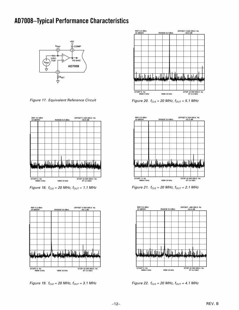
FS ADJUST Full-Scale Adjust Control. A resistor (RSET) is connected between this pin and AGND. This determines the mag-nitude of the full-scale DAC current. The relationship between RSET and the full-scale current is as follows:
IOUTFULL-SCALE (mA) =
6233 ×VREF
RSET VREF = 1.27 V nominal RSET = 390 Ω typical
VREF Voltage Reference Input. A 0.1 µF decoupling ceramic capacitor should be connected between VREF and VAA.There is an internal 1.27 volt reference which can be overdriven by an external reference if required. Seespecifications for maximum range.
COMP Compensation pin. This is a compensation pin for the internal reference amplifier. A 0.1 µF decoupling ceramiccapacitor should be connected between COMP and VAA.
DIGITAL INTERFACE AND CONTROL
CLOCK Digital Clock Input for DAC and NCO. DDS output frequencies are expressed as a binary fraction of the fre-quency of this clock. The output frequency accuracy and phase noise is determined by this clock.
FSELECT Frequency Select Input. FSELECT controls which frequency register, FREQ0 or FREQ1, is used in the phaseaccumulator. Frequency selection can be done on a cycle-per-cycle basis. See Tables I, II and III.
LOAD Register load, active high digital Input. This pin, in conjunction with TC3–TC0, control loading of internal regis-ters from either the parallel or serial assembly registers. The load pin must be high at least 1t1. See Table II.
TC3–TC0 Transfer Control address bus, digital inputs. This address determines the source and destination registers that areused during a transfer. The source register can either be the parallel assembly register or the serial assembly regis-ter. The destination register can be any of the following: COMMAND REG, FREQ0 REG, FREQ1 REG,PHASE REG or IQMOD REG. TC3–TC0 should be valid prior to LOAD rising and should not change untilLOAD falls. The Command Register can only be loaded from the parallel assembly register. See Table II.
CS Chip Select, active low digital input. This input in conjunction with WR is used when writing to the parallelassembly register.
WR Write, active low digital input. This input in conjunction with CS is used when writing to the parallel assemblyregister.
D7–D0 Data Bus, digital inputs. These represent the low byte of the 16-bit data input port used to write to the 32-bitparallel assembly register. The databus can configured for either a 8-bit or 16-bit MPU/DSP ports.
D15–D8 Data Bus, digital inputs. These represent the high byte of the 16-bit data input port used to write to the 32-bitparallel assembly register. The databus can be configured for either a 8-bit or 16-bit MPU/DSP ports. When thedatabus is configured for 8-bit operation, D8–D15 should be tied to DGND.
SCLK Serial Clock, digital input. SCLK is used, in conjunction with SDATA, to clock data into the 32-bit serial assem-bly register.
SDATA Serial Data, digital input. Serial data is clocked on the rising edge of SCLK, Most Significant Bit (MSB) first.
SLEEP Low power sleep control, active high digital input. SLEEP puts the AD7008 into a low power sleep mode. Inter-nal clocks are disabled, while also turning off the DAC current sources. A SLEEP bit is also provided in theCOMMAND REG to put the AD7008 into a low power sleep mode.
RESET Register Reset, active high digital input. RESET clears the COMMAND REG and all the modulation registers tozero.
TEST Test Mode. This is used for factory test only and should be left as a No Connect.

REV. B–6–
AD7008
AD7008REGISTER
ANDCONTROL
LOGIC
32
12
20
32
12
PHASEACCUMULATOR
ACCUM RESET
SLEEP
AM ENABLE
PHASESUMMATION
12
SIN
COS
ROM
10
10
10
10
DAC
10
SIN/ COSSUMMATION
11 PIPELINE DELAYS
13 PIPELINE DELAYS
9:0 19:10
IOUT/ IOUT
14 PIPELINE DELAYS
Figure 7. AD7008 CMOS DDS Modulator (See Table I)
CS (27)
D0-D15
(19-26, 8-15)
TC0-TC3
ACCUMULATOR
RESET
CLK
D Q
x 6
D Q
x 6
D Q
x 6
D Q
x 6
D Q
x 6
PASS
1
0x 6
CLK
LOAD (36)
FSEL (31)
(32-35)
D Q D Q D Q
CLK
RESET (38)
RESET SYNCHRONIZATION
TRANSFER CONTROL (TC) REGISTER
CLK
D Q
x 5
TC0TC1
LOAD
TC3
TC2
D Q
TC3
TC2
0123
4
S
E
0123
2
3
4
D Qx 20
E
FREQ 0
FREQ 1
FREQUENCYREGISTERS
PHASE REGISTER
D Qx 12
E
CLK
D Qx 32
E
IQ MOD REGISTER
1
0x32
TO PHASE
SUMMATION
TO SIN/COS
SUMMATION
TO PHASE
ACCUMULATOR
CLK
CLK
CLK
32
32
12
10
TRANSFER DECODE
FSELECT
CLOCK (30)
x 5
D FLIP-FLOPS ARE MASTER SLAVE,LATCHING DATA ON CLK RISING EDGE.
CLK1
0x 24
WR (16)
SCLK (41)
SDATA (42)
SLEEP (37)
15:0 23:8
15:8 7:0
23:0
7:0D Q
x 32
32-BIT SERIALASSEMBLY REGISTER
32-BIT PARALLELASSEMBLY REGISTER
D Q
x 32
REGISTERMUX
31:0
31:0 D Q
x 4
D QCLK
3:0
1
0x 32
D Q D1
D2
BUS MODE
SYNCHRO LOGIC
D0
D3
D Q
D Q
CLK
AM ENABLE
SLEEP
COMMAND REGISTER
CLK
CLK
PASS FLIP-FLOPS ARE TRANSPARENTWHEN THE CLOCK IS LOW.
CLK
01
31:8
D Qx 32
E
5
6
Figure 8. AD7008 Register and Control Logic

AD7008
REV. B –7–
Table II. Source and Destination Register
TC3 TC2 TC1 TC0 LOAD Source Register Destination Register
X X X X 0 N/A N/A0 0 X X 1 Parallel COMMAND*1 0 0 0 1 Parallel FREQ01 0 0 1 1 Parallel FREQ11 0 1 0 1 Parallel PHASE1 0 1 1 1 Parallel IQMOD1 1 0 0 1 Serial FREQ01 1 0 1 1 Serial FREQ11 1 1 0 1 Serial PHASE1 1 1 1 1 Serial IQMOD
*The Command Register can only be loaded from the parallel assembly registers.
Table III. AD7008 Control Registers
Register Size Reset State Description
COMMAND REG* 4 Bits CR3–CR0 All Zeros Command Register. This is written to using the parallel assembly register.FREQ0 REG 32 Bits DB31–DB0 All Zeros Frequency Register 0. This defines the output frequency, when
FSELECT = 0, as a fraction of the CLOCK frequency.FREQ1 REG 32 Bits DB31–DB0 All Zeros Frequency Register 1. This defines the output frequency, when
FSELECT = 1, as a fraction of the CLOCK frequency.PHASE REG 12 Bits DB11–DB0 All Zeros Phase Offset Register. The contents of this register is added to the
output of the phase accumulator.IQMOD REG 20 Bits DB19–DB0 All Zeros I and Q Amplitude Modulation Register. This defines the amplitude of
the I and Q signals as 10-bit twos complement binary fractions.DB[19:10] is multiplied by the Quadrature (sine component andmultiplied by the In-Phase (cosine) component.
*On power up, the Command Register should be configured by the user for the desired mode before operation.
Table IV. Command Register Bits*
CR0 = 0 Eight-Bit Databus. Pins D15–D8 are ignored and the parallel assembly register shifts eight places left on each write.Hence four successive writes are required to load the 32-bit parallel assembly register, Figure 6.
= 1 Sixteen-Bit Databus. The parallel assembly register shifts 16 places left on each write. Hence two successive writes arerequired to load the 32-bit parallel assembly register, Figure 5.
CR1 = 0 Normal Operation.= 1 Low Power Sleep Mode. Internal Clocks and the DAC current sources are turned off.
CR2 = 0 Amplitude Modulation Bypass. The output of the sine LUT is directly sent to the DAC.= 1 Amplitude Modulation Enable. IQ modulation is enabled allowing AM or QAM to be performed.
CR3 = 0 Synchronizer Logic Enabled. The FSELECT, LOAD and TC3–TC0 signals are passed through a 4-stage pipelineto synchronize them with the CLOCK, avoiding metastability problems.
= 1 Synchronizer Logic Disabled. The FSELECT, LOAD and TC3–TC0 signals bypass the synchronization logic. Thisallows for faster response to the control signals.
*The Command Register can only be loaded from the parallel assembly register.
Table I. Latency Table
LatencyFunction (Synchronizer Enabled CR3 = 01)
FSelect 14t1
Phase 13t1
IQ Mod 11t1
NOTE1All latencies are reduced by 4t1 when CR3 = 1 (synchronizer disabled). 1t1 is equal to one pipeline delay.

REV. B–8–
AD7008CIRCUIT DESCRIPTIONThe AD7008 provides an exciting new level of integration forthe RF/Communications system designer. The AD7008 com-bines the numerically controlled oscillator (NCO), SINE/CO-SINE look-up tables, frequency, phase and IQ modulators, anda digital-to-analog converter on a single integrated circuit.
The internal circuitry of the AD7008 consists of four main sec-tions. These are:
Numerically Controlled Oscillator (NCO) + Phase ModulatorSINE and COSINE Look-Up TablesIn Phase and Quadrature ModulatorsDigital-to-Analog Converter
The AD7008 is a fully integrated Direct Digital Synthesis(DDS) chip. The chip requires one reference clock, two low-precision resistors and six decoupling capacitors to providedigitally created sine waves up to 25 MHz. In addition to thegeneration of this RF signal, the chip is fully capable of a broadrange of simple and complex modulation schemes. Thesemodulation schemes are fully implemented in the digital domainallowing accurate and simple realization of complex modulationalgorithms using DSP techniques.
THEORY OF OPERATIONSine waves are typically thought of in terms of their amplitudeform: a(t) = sin (ωt) or a(t) = cos (ωt). However, these are non-linear and not easy to generate except through piece wise con-struction. On the other hand, the angular information is linearin nature. That is, the phase angle rotates though a fixed anglefor each unit of time. The angular rate depends on the fre-quency of the signal by the traditional rate of: ω = 2 πf.
+1
0
–1
2π
0
MAGNITUDE
PHASE
Figure 9.
Knowing that the phase of a sine wave is linear and given a ref-erence interval (clock period), the phase rotation for that periodcan be determined.
∆Phase = ωdt
Solving for w:
ω = ∆Phase
dt= 2 πf
Solving for f and substituting the reference clock frequency for
the reference period:
1fCLOCK
= dt
:
f =∆Phase × fCLOCK
2 π
The AD7008 builds the output based on this simple equation.A simple DDS chip will implement this equation with 3 majorsubcircuits. The AD7008 has an extra section for I and Qmodulation.
Numerically Controlled Oscillator + Phase ModulatorThis consists of two frequency select registers, a phase accumu-lator and a phase offset register. The main component of theNCO is a 32-bit phase accumulator which assembles the phasecomponent of the output signal. Continuous time signals have aphase range 0 to 2 π. Outside this range of numbers, the sinu-soidal functions repeat themselves in a periodic manner. Thedigital implementation is no different. The accumulator simplyscales the range of phase numbers into a multibit digital word.The phase accumulator in the AD7008 is implemented with 32bits. Therefore in the AD7008, 2 π = 232
. Likewise, the ∆Phaseterm is scaled into this range of numbers 0 ≤ ∆Phase ≤ 232 – 1.Making these substitutions into the equation above:
f = ∆Phase × fCLOCK
232where 0 ≤ ∆Phase < 232
With a clock signal of 50 MHz and a phase word of 051EB852hex:
f = 51EB852 × 50 MHz
232= 1.000000000931 MHz
The input to the phase accumulator (i.e., the phase step) can beselected either from the FREQ0 Register or FREQ1 Register,and this is controlled by the FSELECT pin. The phase accu-mulator in the AD7008 inherently generates a continuous 32-bit phase signal, thus avoiding any output discontinuity whenswitching between frequencies. This facilitates complex fre-quency modulation schemes, such as GMSK.
Following the NCO, a phase offset can be added to performphase modulation using the 12-bit PHASE Register. The con-tents of this register are added to the most significant bits of theNCO.
Sine and Cosine Look-Up TablesTo make the output useful, the signal must be converted fromphase information into a sinusoidal value. Since phase informa-tion maps directly into amplitude, a ROM look up table con-verts the phase information into amplitude. To do this thedigital phase information is used to address a Sine/Cosine ROMLUT. Only the most significant 12 bits are used for this pur-pose. The remaining 20 bits provide frequency resolution andminimize the effects of quantization of the phase to amplitudeconversion.
In Phase and Quadrature ModulatorsTwo 10-bit amplitude multipliers are provided allowing the easyimplementation of either Quadrature Amplitude Modulation(QAM) or Amplitude Modulation (AM). The 20-bit IQMODRegister is used to control the amplitude of the I (cos) and Q(sin) signals. IQMOD [9:0] controls the I amplitude andIQMOD [19:10] controls the Q amplitude.
The user should ensure that when summing the I and Q signalsthe sum should not exceed the value that a 10-bit accumulatorcan hold. The AD7008 does not clip the digital output; theoutput will roll over instead of clip.

AD7008
REV. B –9–
When amplitude modulation is not required, the IQ multiplierscan be bypassed (CR = 2). The sine output is directly sent tothe 10-bit DAC.
Digital-to-Analog ConverterThe AD7008 includes a high impedance current source 10-bitDAC, capable of driving a wide range of loads at differentspeeds. Full-scale output current can be adjusted, for optimumpower and external load requirements, through the use of asingle external resistor (RSET).
The DAC can be configured for single or differential-endedoperation. IOUT can be tied directly to AGND for single-endedoperation or through a load resistor to develop an output volt-age. The load resistor can be any value required as long as thefull-scale voltage developed across it does not exceed 1 volt.Since full-scale current is controlled by RSET, adjustments toRSET can balance changes made to the load resistor.
DSP and MPU InterfacingThe AD7008 contains a 32-bit parallel assembly register and a32-bit serial assembly register. Each of the modulation registerscan be loaded from either assembly register under control of theLOAD pin and the Transfer-Control (TC) pins (See Table II).The Command register can be loaded only from the parallel as-sembly register. In practical use, both serial and parallel inter-faces can be used simultaneously if the application requires.
TC3–TC0 should be stable before the LOAD signal rises andshould not change until after LOAD falls (Figure 2).
The DSP/MPU asserts both WR and CS to load the parallel as-sembly register (Figure 3). At the end of each write, the parallelassembly register is shifted left by 8 or 16 bits (Depending onCR0), and the new data is loaded into the low bits. Hence, two16-bit writes or four 8-bit writes are used to load the parallel as-sembly register. When loading parallel data, it is only necessaryto write as much data as will be used by that register. For in-stance, the Command Register requires only one write to theparallel assembly register.
Serial data is input to the chip on the rising edge of SCLK, mostsignificant bit first (Figure 4). The data in the assembly regis-ters can be transferred to the modulation registers by means ofthe transfer control pins.
Maximum Updating of the AD7008Updating the AD7008 need not take place in a synchronousfashion. However, in asynchronous systems, most of the exter-nal clock pulses (LOAD and SCLK) must be high for greaterthan one system clock period. This insures that at least oneCLOCK rising edge will occur successfully completing the latchfunction (Figure 1).
However, if the AD7008 is run in a synchronous mode with thecontrolling DSP or microcontroller, the AD7008 may be loadedvery rapidly. Optimal speed is attained when operated in the16-bit load mode; the following discussion will assume thatmode is used. Each of the modulation registers require two 16bit loads. This data is latched into the parallel assembly registeron the falling edge of the WR command. This strobe is notqualified by the CLOCK pulse but must be held low for a mini-mum of 20 ns and only need be high for 10 ns. The two 16-bitwords may be loaded in succession. While the second 16-bitword is being latched into the parallel assembly register, theTransfer and Control word may be presented to the TC3–TC0pins. If the designation register is always the same, an externalregister can be used to store the information on the inputs of
TC3–TC0. At some time after the second falling edge of WR,the LOAD signal may go high. As long as the load signal is high5 ns (see setup time) before the rising edge of the CLOCK sig-nal, data will be transferred to the destination register.
The limiting factor of this technique is the WR period which is30 ns. Thus the CLOCK may run up to 33 MSPS using thistechnique and the effective update rate would be one half or16.5 MHz. See timing Figure 10 for timing details.
DATA HI WORD
WR
LOW WORD
CLOCK
TC
LOAD
Figure 10. Accelerated Data Load Sequence
APPLICATIONSSerial ConfigurationData is written to the AD7008 in serial mode using the two sig-nal lines SDATA and SCLK. Data is accumulated in the serialassembly register with the most significant bit loaded first. Thedata bits are loaded on the rising edge of the serial clock. Oncedata is loaded in the serial assembly register, it must be trans-ferred to the appropriate register on chip. This is accomplishedby setting the TC bits according to Tables II and III. If youwant to load the serial assembly register into FREQ1 register,the TC bits should be 1101. When the LOAD pin is raised,data is transferred directly to the FREQ1 register. When oper-ating in serial mode, some functions must still operate in parallelmode such as loading the TC bits and updating the Commandregister which is accessed only through the parallel assemblyregister. See Figure 11 for a typical serial mode configuration.
R5
390
C2
0.1µF
CMD0CMD1CMD2CMD3
192021222324252689
10111213141516
D0D1D2D3D4D5D6D7D8D9D10D11D12D13D14D15WR
TC0TC1TC2TC3
WR
LOADSCLK
SDATA
RESET
VCC
VEE
50MHzU2
+5V
K11157
14
OUT
VREF
COMP
IOUT
IOUT
FSADJUST
VAAVDDVDDVDD
AGNDDGNDDGNDDGNDDGND
TEST
447182943
40
3172839
+5V+5V+5V+5V
4
5
6C1
0.1µF+5V
+5V
R4
49.9
2
1 R3
49.9
U3AD7008
8
TC0TC1TC2TC3LOADSCLKSDATAFSELECTCLKRESETSLEEP
CS273233343536414231303837
Figure 11. General Purpose Serial Interface

REV. B–10–
AD7008Parallel ConfigurationThe AD7008 functions fully in the parallel mode. There aretwo parallel modes of operation. Both are similar but are tai-lored for different bus widths, 8 and 16 bits. All modes of op-eration can be controlled by the parallel interface.
On power up and reset, the chip must be configured by instruc-ting the command register how to operate. The command reg-ister may be used to set the device up for 8- or 16-bit mode,
RFINPUT
(ANTENNA)330Ω 330Ω
4.7µF
100nF
100nF
MIDPOINTBIAS
GENERATOR
OPTIONALBPF
OR LPF
VMID10Ω
10Ω
BANDPASSFILTER
AGCDETECTOR
PLL
90°
0°
FM OUTPUT
AM OUTPUT
BIASCIRCUIT PTAT
VOLTAGE
AGC VOLTAGE
PLL INPUT
RECEIVEDSIGNALSTRENGTHINDICATOR
RSET390Ω
5Ω 5Ω
AD7008
FILTER
0.1µF–16dBm
10 BITS
AD607
Figure 13. AD7008 and AD607 Receiver Circuit
sleep mode, amplitude control and synchronization logic. Atreset, the chip defaults to 8-bit bus, no amplitude control andlogic synchronized. The code fragment below indicates howthe initialization code for the AD7008 might look using theADSP-21020.
dds_para is a port define to decode forthe parallel assembly register write pulse.dds_cont is a port defined to decode forthe TC control Load pin. The Command reg-ister must first be loaded with configura-tion information. In this example, the chipis set up for 16 bits data. See Table IIIfor details.
r4 = 0x00010000; 16 bits, Normal Op., AMdisabled, Synchronizerenabled
dm(dds_para) = r4; write data to parallelassembly register
r4 = 0x00000000;dm(dds_cont) = r5; No data written, data is
just transferred fromparallel assemblyregister to the commandregister
r4 = 0x051E0000; 1 MHz=051EB852, load highword first
dm(dds_para) = r4;r4 = 0xB8520000; Now load low worddm(dds_para)=r4;r4 = 0x80000000; Transfer data from the
parallel assemblyregister to Freq0
dm(dds_cont)=r4;
Local OscillatorThe AD7008 is well suited for applications such as local oscilla-tors used in super-heterodyne receivers. Although the AD7008can be used in a variety of receiver designs, one simple local os-
C1
0.1µF
645
Y7Y6Y5Y4Y3Y2Y1Y0
79
101112131415
G1G2AG2B
+5VDMS1
DMWR
R5
390
C2
0.1µF
DMD24DMD25DMD26DMD27DMD28DMD29DMD30DMD31DMD32DMD33DMD34DMD35DMD36DMD37DMD38DMD39
192021222324252689
10111213141516
TC0TC1TC2TC3LOADSCLKSDATAFSELECTCLKRESETSLEEP
CSGNDDMD36DMD37DMD38DMD39
RESETVCC
VEE
50MHzU2
+5V
K11157
14
OUT
VREF
COMP
IOUT
IOUT
FSADJUST
VAAVDDVDDVDD
AGNDDGNDDGNDDGNDDGND
TEST
447182943
40
3172839
+5V+5V+5V+5V
4
5
6 +5V
+5V
R4
49.9
2
1R3
49.9
CBA
DMA02DMA01DMA00
321
U174HC138
U3AD7008
8
DMDXX–DATA BITSDMAXX–ADDRESS BITS
D0D1D2D3D4D5D6D7D8D9D10D11D12D13D14D15WR
273233343536414231303837
Figure 12. Parallel Interface to a 16- or 32-Bit DSP or
Microprocessor

AD7008
REV. B –11–
This section converts the twos complement au-dio into offset binary scaled for modulatingthe AD7008. If twos complement is used, themodulation scheme will instead be double side-band, suppressed carrier.
r5 = 0x80000000;r6 = r6 xor r5;r6 = lshift r6 by -1;r6 = r6 xor r5;r4 = lshift r6 by -6;
Load parallel assembly register with modula-tion data. Q portion set to midscale, Iportion with scaled data
r5 = 0x00000004;dm(dds_para) = r5;dm(dds_para) = r4;
Transfer parallel assembly register to IQMODregister
r4 = 0xb0000000;dm(dds_cont) = r4;rti;
Many applications require precise control of the output ampli-tude, such as in local oscillators, signal generators and modula-tors. There are several methods to control signal amplitude.The most direct is to program the amplitude using the IQMODregister on the AD7008. Other methods include selecting theload resistor value or changing the value of RSET. Another op-tion is to place a voltage out DAC on the ground side of RSET asin Figure 16. This allows easy control of the output amplitudewithout affecting other functions of the AD7008. Any combina-tion of these techniques may be used as long as the full-scalevoltage developed across the load does not exceed 1 volt.
cillator application is with the AD607 Monoceiver(tm). Thisunique two chip combination provides a complete receiver sub-system with digital frequency control, RSSI and demodulatedoutputs for AM, FM and complex I/Q (SSB or QAM). (SeeFigure 13.)
Direct Digital ModulatorIn addition to the basic DDS function provided by the AD7008,the device also offers several modulation capabilities useful in awide variety of application. The simplest modulation scheme isfrequency shift keying or FSK. In this application, each of thetwo frequency registers is loaded with a different value, one rep-resenting the space frequency and the other the mark frequency.The digital data stream is fed to the FSELECT pin causingthe AD7008 to modulate the carrier frequency between the twovalues.
FREQ 0REG
FREQ 1REG
32
32
32MUX
32
0
1 1
0 0
F SELECT CLOCK
PHASEACCUMULATOR
AD7008
Figure 14. FSK Modulator
The AD7008 has three registers that can be used for modula-tion. Besides the example of frequency modulation shownabove, the frequency registers can be updated dynamically ascan the phase register and the IQMOD register. These can bemodulated at rates up to 16.5 MHz. The example shown belowalong with code fragment shows how to implement the AD7008in an amplitude modulation scheme. Other modulationschemes can be implemented in a similar fashion.
SIN/COSROM
SIN
COS
DSP:SCALE
ANALOGINPUT TO
FULLSCALE
I MODADC
Q MOD
10 10
10
1010
10
10-BIT DAC
IOUT
IOUT10
10
0AD7008
Figure 15. Amplitude Modulation
__________IRQ3 Interrupt Vector__________
in_audio is a port used to sample the audiosignal. This signal is assumed to be twoscomplement. This interrupt should be servicedat an audio sample rate. This routine assumesthat the AD7008 has been set up with the Ampli-tude Modulation Enabled.
irq3_asserted:Get audio sample
r6=dm(in_audio);
C1
0.1µF
645
Y7Y6Y5Y4Y3Y2Y1Y0
79
101112131415
G1G2AG2B
+5VDMS1
DMWR
R5
390
C2
0.1µF
DMD24DMD25DMD26DMD27DMD28DMD29DMD30DMD31DMD32DMD33DMD34DMD35DMD36DMD37DMD38DMD39
192021222324252689
10111213141516
DMS3DMD36DMD37DMD38DMD39
RESETVCC
VEE
50MHzU2
+5V
K11157
14
OUT
VREF
COMP
IOUT
IOUT
FSADJUST
VAAVDDVDDVDD
AGNDDGNDDGNDDGNDDGND
TEST
447182943
40
3172839
+5V+5V+5V+5V
4
5
6 +5V
+5V
R4
49.9
2
1R3
49.9
CBA
DMA02DMA01DMA00
321
U174HC138
U3AD7008
8
VOLTAGE OUT DAC,i.e., AD7245A
0 TO +1 VOLTSIfs =6233 x (VREF –VDAC)
RSET
DMDXX–DATA BITSDMAXX–ADDRESS BITS
CS
TC0TC1TC2TC3LOADSCLKSDATAFSELECTCLKRESETSLEEP
D0D1D2D3D4D5D6D7D8D9D10D11D12D13D14D15WR
273233343536414231303837
Figure 16. External Gain Adjustment
AD7008–Typical Performance Characteristics
START 0 Hz RBW 3 kHz VBW 10 kHz
STOP 10 000 000.0 HzST 2.4 SEC
REF 5.0 dBm10 dB/DIV RANGE 5.0 dBm
OFFSET 4 640 000.0 Hz–54.8 dB
Figure 20. fCLK = 20 MHz, fOUT = 5.1 MHz
START 0 Hz RBW 3 kHz VBW 10 kHz
STOP 10 000 000.0 HzST 2.4 SEC
REF 4.3 dBm10 dB/DIV RANGE 5.0 dBm
OFFSET 6 320 000.0 Hz–61.3 dB
Figure 21. fCLK = 20 MHz, fOUT = 2.1 MHz
START 0 Hz RBW 3 kHz VBW 10 kHz
STOP 10 000 000.0 HzST 2.4 SEC
REF 5.0 dBm10 dB/DIV RANGE 5.0 dBm
OFFSET –490 000.0 Hz–63.4 dB
Figure 22. fCLK = 20 MHz, fOUT = 4.1 MHz
REV. B–12–
VREF
6
4
5
VREF
+5V
TO DAC
COMP
RSET
AD7008
115ΩTYP
Figure 17. Equivalent Reference Circuit
START 0 Hz RBW 3 kHz VBW 10 kHz
STOP 10 000 000.0 HzST 2.4 SEC
REF 4.3 dBm10 dB/DIV RANGE 5.0 dBm
OFFSET 3 330 000.0 Hz–63.6 dB
Figure 18. fCLK = 20 MHz, fOUT = 1.1 MHz
START 0 Hz RBW 3 kHz VBW 10 kHz
STOP 10 000 000.0 HzST 2.4 SEC
REF 4.3 dBm10 dB/DIV RANGE 5.0 dBm
OFFSET 4 500 000.0 Hz–61.1 dB
Figure 19. fCLK = 20 MHz, fOUT = 3.1 MHz

START 0 Hz RBW 3 kHz VBW 10 kHz
STOP 10 000 000.0 HzST 2.4 SEC
REF 5.0 dBm10 dB/DIV RANGE 5.0 dBm
OFFSET 1 680 000.0 Hz–52.8 dB
Figure 23. fCLK = 20 MHz, fOUT = 6.1 MHz
CENTER 6 500 000.0 Hz RBW 3 kHz VBW 10 kHz
SPAN 10 000 000.0 HzST 2.4 SEC
REF 4.3 dBm10 dB/DIV RANGE 5.0 dBm
OFFSET 500 000.0 Hz–51.7 dB
Figure 24. fCLK = 20 MHz, fOUT = 6.5 MHz
VBW 10 kHzSTOP 16 000 000.0 Hz
ST 3.6 SEC
REF 4.3 dBm10 dB/DIV RANGE 5.0 dBm
OFFSET 6 304 000.0 Hz–56.3 dB
START 0 Hz RBW 3 kHz
Figure 25. fCLK = 50 MHz, fOUT = 2.1 MHz
CENTER 16 000 000.0 Hz RBW 3 kHz
REF 4.3 dBm10 dB/DIV RANGE 5.0 dBm
OFFSET 14 500 000.0 Hz–52.4 dB
VBW 10 kHzSPAN 25 000 000.0 Hz
ST 5.6 SEC
Figure 26. fCLK = 50 MHz, fOUT = 7.1 MHz
VBW 10 kHzSTOP 10 000 000.0 Hz
ST 2.4 SEC
REF 5.0 dBm10 dB/DIV RANGE 5.0 dBm
OFFSET –1 280 000.0 Hz –51.8 dB
START 0 Hz RBW 3 kHz
Figure 27. fCLK = 20 MHz, fOUT = 7.1 MHz
VBW 10 kHzSTOP 25 000 000.0 Hz
ST 5.6 SEC
REF 4.3 dBm10 dB/DIV RANGE 5.0 dBm
START 0 Hz RBW 3 kHz
OFFSET 15 300 000.0 Hz–51.8 dB
Figure 28. fCLK = 50 MHz, fOUT = 5.1 MHz
Typical Performance Characteristics–AD7008
REV. B –13–
START 0 Hz RBW 3 kHz VBW 10 kHz
STOP 25 000 000.0 HzST 5.6 SEC
REF 5.0 dBm10 dB/DIV RANGE 5.0 dBm
OFFSET 4 500 000.0 Hz–54.7 dB
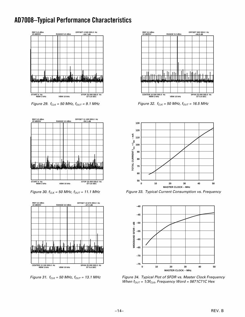
Figure 29. fCLK = 50 MHz, fOUT = 9.1 MHz
START 0 Hz RBW 3 kHz VBW 10 kHz
STOP 25 000 000.0 HzST 5.6 SEC
REF 5.0 dBm10 dB/DIV RANGE 5.0 dBm
OFFSET 11 100 000.0 Hz–54.1 dB
CENTER 13 100 000.0 Hz RBW 3 kHz VBW 10 kHz
SPAN 25 000 000.0 HzST 5.6 SEC
REF 5.0 dBm10 dB/DIV RANGE 5.0 dBm
OFFSET 10 675 000.0 Hz–47.0 dB
Figure 31. fCLK = 50 MHz, fOUT = 13.1 MHz
Figure 30. fCLK = 50 MHz, fOUT = 11.1 MHz
CENTER 16 500 000.0 Hz RBW 3 kHz VBW 10 kHz
SPAN 25 000 000.0 HzST 5.6 SEC
REF 5.0 dBm10 dB/DIV RANGE 5.0 dBm
OFFSET 500 000.0 Hz–44.8 dB
130
5050
70
60
100
90
80
100
110
120
403020
MASTER CLOCK – MHz
TO
TA
L C
UR
RE
NT
I AA
+ I D
D –
mA
Figure 32. fCLK = 50 MHz, fOUT = 16.5 MHz
Figure 33. Typical Current Consumption vs. Frequency
Figure 34. Typical Plot of SFDR vs. Master Clock Frequency
When fOUT = 1/3fCLK, Frequency Word = 5671C71C Hex
–40
–7550
–60
–70
10
–65
0
–45
–55
–50
403020
MASTER CLOCK – MHz
WID
EB
AN
D S
FD
R –
dB
REV. B–14–
AD7008–Typical Performance Characteristics

AD7008
REV. B –15–
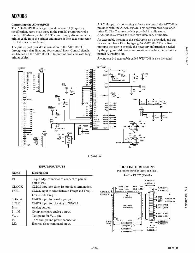
AD7008/PCB DDS EVALUATION BOARDThe AD7008/PCB DDS Evaluation Board allows designers toevaluate the high performance AD7008 DDS Modulator with aminimum amount of effort.
To prove this DDS will meet the user’s waveform synthesis re-quirements, the only things needed are the AD7008/PCB DDSEvaluation Board, +5 V power supply, an IBM-compatible PC,and a spectrum analyzer. The evaluation setup is shown below.
The DDS evaluation kit includes a populated, tested AD7008/PCB board; software which controls the AD7008 through theparallel printer port in a DOS or Windows environment and anAD7008P.
The AD7008 direct digital synthesis chip is a numericallycontrolled oscillator employing a 32-bit phase accumulator, sineand cosine look-up tables, and a l0-bit D/A converter integratedon a single CMOS chip. Modulation capabilities are providedfor phase modulation, frequency modulation, and both in-phaseand quadrature amplitude modulation suitable for SSBgeneration.
Clock rates up to 20 MHz and 50 MHz are supported. Fre-quency accuracy can be controlled to one part in four billion.
+5V
SOFTWAREPROVIDED
POWERSUPPLY
INTERFACE
EXTERNALPOWERSUPPLY
STANDARDPRINTERCABLE
IBM-COMPATIBLE PC
AD700850MHz
CMOS DDSINTERFACE
LOGIC
50Ω CABLE
SPECTRUM ANALYZER
AD7008 DDS EVALUATION BOARD
OPTIONALTTL CLOCKREFERENCEGENERATOR
CLOCKOSCILLATOR
Figure 35. AD7008 DDS Evaluation Board Setup
Table IV. AD7008/PCB Typical Electrical Characteristics(Nominal power supplies, CLK = 50 MHz)
TypicalCharacteristics Value Units
+5.0 V Supply Current 125 mAAD7008 Output Voltage 0 to +1.0 V
(Terminated into 50 Ω Externally)CMOS clock input HIGH 4.1 to 5 VCMOS clock input LOW 0.0 to 0.5 V
USING THE AD7008/PCB DDS EVALUATION BOARD
The AD7008/PCB evaluation kit is a test system designed tosimplify the evaluation of the AD7008 50 MHz Direct DigitalSynthesizer. Provisions to control the AD7008 from the printerport of an IBM-compatible PC are included, along with the
necessary software. This data sheet provides information onoperating the evaluation board; additional details are availablefrom the ADI technical assistance line 1-800-ANALOGD.
Prototyping AreaAn area near one edge of the board is intentionally left void ofcomponents to allow the user to add additional circuits to theevaluation test set. Users may want to build custom analog fil-ters for the outputs, or add buffers and operational amplifiersused in the final applications.
XO vs. External ClockThe reference clock of the AD7008/PCB is normally providedby a 50 MHz CMOS oscillator. This oscillator can be removedand an external CMOS clock connected to CLOCK. If an ex-ternal clock is used, a 50 Ω resistor R6 should be installed.
Power SupplyPower for the AD7008/PCB must be provided externallythrough the pin connections, as described in the Inputs/Outputs.The power leads should be twisted to reduce ground loops.
AD7008/PCB BILL OF MATERIAL
Quantity Reference Description
1 C1 Tag – Tant Cap, 10 µF, 35 V, 20%
8 C2–C9 Cer Chip Cap, 0.1 µF, MurataGrm42
6 CLOCK, FSEL SMB – Submin Snap-on (Male)IOUT, IOUTN PCB MT PlugSCLK, SDATA
1 FSADJ RN55 – Res Met Film, 392
1 LK1 HDR SIP 3-Pin Male
1 Shunt 530153-2
1 P1 36-Pin D Conn Rt Ang PcmtFem AMP
1 P2 PC Voltage Ter Blk w/ScrewsAugat RDI
3 R1–R3 RN55 – Res Met Film, 10k
2 R4, R5 RN55 – Res Met Film, 49.9
1 RZ1 10P Bussed Res Ntwk, 10kCSC10A01103G
1 RZ2 6P Bussed Res Ntwk, 4.7kCSC06A01472G
1 U1 AD7008 JP50 CMOS DDS
Modulator
1 U2 74HC74 – Dual D-type Pos-Ed-Trigd Flip-Flop
1 VREF Pin Terminal, Testpoint
1 XTAL OSC XTAL, Fox F1100H50 MHz
1 Socket, Methode 213-044-501
4 Support, Nylon
1 PCB, 48295(-)
26 Pin Sockets, Closed End
REV. B–16–
AD7008A 3.5" floppy disk containing software to control the AD7008 isprovided with the AD7008/PCB. This software was developedusing C. The C source code is provided in a file namedA:\AD7008.C, which the user may view, run, or modify.
An executable version of this software is also provided, and canbe executed from DOS by typing “A:\AD7008.” The softwareprompts the user to provide the necessary information neededby the program. Additional information is included in a test filenamed A:\readme.txt.
A windows 3.1 executable called WIN7008 is also included.
OUTLINE DIMENSIONSDimensions shown in inches and (mm).
44-Pin PLCC (P-44A)
6
PIN 1IDENTIFIER
740
39
1718
2928
TOP VIEW(PINS DOWN)
0.695 (17.65)0.685 (17.40) SQ
0.656 (16.66)0.650 (16.51) SQ
0.048 (1.21)0.042 (1.07)
0.048 (1.21)0.042 (1.07)
0.020(0.50)
R
0.021 (0.53)0.013 (0.33)
0.050(1.27)BSC
0.63 (16.00)0.59 (14.99)
0.032 (0.81)0.026 (0.66)
0.180 (4.57)0.165 (4.19)
0.040 (1.01)0.025 (0.64)
0.056 (1.42)0.042 (1.07)
0.025 (0.63)0.015 (0.38)
0.110 (2.79)0.085 (2.16)
INPUTS/OUTPUTS
Name Description
P1 36-pin edge connector to connect to parallelport of PC.
CLOCK CMOS input for clock R6 provides termination.FSEL CMOS input to select between Freq 0 and Freq 1.
Low selects Freq 0.SDATA CMOS input for serial input pin.SCLK CMOS input for clocking in SDATA.IOUT Analog output.IOUTN Complementary analog output.VREF Test point for VREF pin.P2 +5 V and ground power connection.LK1 External sleep command input.
Figure 36.
Controlling the AD7008/PCBThe AD7008/PCB is designed to allow control (frequencyspecification, reset, etc.) through the parallel printer port of astandard IBM-compatible PC. The user simply disconnects theprinter cable from the printer and inserts it into edge connectorP1 of the evaluation board.
The printer port provides information to the AD7008/PCBthrough eight data lines and four control lines. Control signalsare latched on the AD7008/PCB to prevent problems with longprinter cables.
PR
INT
ED
IN
U.S
.A.
C1
79
1a
–1
0–2
/95
VCC
OUT
+5V 14
7
XTAL1
8C9
0.1µF
VEE
PRQ
QCLC
D
>
PRQ
QCLC
D
>LATCH
LOAD2
3
4
5
6
8
9
10
11
12
13
1
LLOAD
WR
+5V
+5V
+5V+5V U2
74HC74
U274HC74
LWR
C36DRPFP1
12345678910111213
1415161718192021222324252627282930313233343536
LATCHD0D1D2D3D4D5
D7D6
RESET
LOAD
WR
23456789
10
D0D1D2D3D4D5
D7D6
10k10PB+5
RZ1
23456
LATCHRESETLOAD
WR
4.7k6PB+5
RZ2
U1DUT7008P
6
5
2
1
4
3172839
447182943
40
VREF
COMP
FSADJUST
1920212223242526
89
10111213
14151627323334353641423130
3837
D0D1D2D3D4D5
D7D6
RESET
123
H3MLK1
+5V
GND
+5V
+5VD
12
P2PCTB2
D8D9D10D11D12D13
D15D14
R110k
SMBSCLK
R210k
R310k
SMBFSELECT
R650OPTIONAL
WR
CS
TC0
TC2TC1
TC3LOAD
SCLKSDATAFSELECTCLK
SLEEP
D0
D1D2D3
LLOAD
RESET
DGNDDGNDDGNDDGND
AGND
TEST
+5V+5V+5V+5V
C70.1µF
+5V
R450
SMBIOUT
FSADJ
390
LWR
SMBSDATA
SMBCLK
IOUT
IOUT
VREF
SMBIOUTR5
50
C60.1µF
C20.1µF
C30.1µF
C40.1µF
C50.1µF
C110µF
C80.1µF
D0D1D2D3D4D5
D7
D6
VAAVDDVDDVDD


