
99
AUTOMATED DESIGN OF INDUSTRIAL SEQUENCE CONTROLLERS
R. Tabachnick**, T. Le-Ngoct, L.J. Vroomen*, and P.J. Zsombor-Murray*
*DATAC computer Laboratory, McGill University tSPAR Aerospace Ltd. +The Bailey Meter Company
ABSTRACT
A system for replacing solid-state or relay based industrial control logic with custom firmware, implemented in a standard system is described. A comparison to other approaches, such as OEM implemented high level language based systems and large computer based systems is made. Existing software developments, particularly high level languages for user convenience, are discussed. The approach includes three principal concepts, viz:(1) A high level user-oriented programming language which allows the
designer to describe an entire logic circuit with a series of keystrokes.
(2) A compiler which generates object code for a standard microprocessor based controller unit, and
(3) A microprocessor based, portable suitcase, development system which includes all the necessary hardware and firmware for field implementation and modification of sequence controllers. The portable development system is based on the Motorola MC6800
microprocessor family while the controller uses the Motorola MCI4500B I-bit microprocessor family. The development of the keystroke language and its compiler/interpreter.
AUTOMATISATION DE LA MISE EN APPLICATION DES CONTROLEURS INDUSTRIELS DE MISE EN S~QUENCE
Un systeme pour remplacer les controles industriels logiques a composants semi-conducteurs ou a relais par une microprogrammation adaptee aux besoins particuliers de l'utilisateur d'un systeme standard est decrit. L'on fait la comparaison entre les autres methodes telles que la mise en application O.E.M. des systemes a langage de programmation evolue et des systemes a base de gros ordinateurs. D'autres concepts de software et particulierement les langages evolues pour la convenance de l'usager sont trait~s. Les trois concepts principals de cette approche sont: (1) Un langage de programmation evolue oriente vers l'usager qui permet
un concept decrivant un circuit logique entier au moyen d'un clavier. (2) Un compilateur produisant un code pour un controleur standard
microprocesseur. (3) Un systeme portatif a microprocesseur qui comprend tout le hardware
et la microprogrammation necessaire pour la mise en application et la modification sur le chantier des controleurs de mise en sequence. La realisation du systeme portatif est basee sur la famille de micro
processeurs Motorola MC6800 et le controleur utilise la famille de microprocesseurs Motorola MCI4500B I-bit. La mise en valeur du langage du clavier et de son compilateur/interpreteur est accentuee.
100
AUTOMATED DESIGN OF INDUSTRIAL SEQUENCE CONTROLLERS
by
R. Tabachnick, T. Le-Ngoc, &.J. Vroomen and P.J. Zsombor-MUrray
INTRODUCTION
Programmable sequence controllers were developed to reduce the cost involved in relay or solid state based sequence controller implementations. In order to understand the problem, consider the steps required to develop a "hardwired" sequencing system:-
1. Definition of the sequences, 2. Design of the functional circuits, 3. Fabrication of component circuit subassemb1ies, 4. Testing them, 5. System integration, 6. Testing the entire system and 7. Installation and startup.
Steps 1., 6. and 7. are required regardless of the technology upon which a sequence controller design is based. In programmable controllers, software writing and debugging represent steps 2., 3. and 4. By anticipating features common to the entire class of applications for which a sequence controller is intended, system integration, step 5., can be standardized to include all functions, whether they are required for a given application or not. The waste of an unused function is more than outweighed by eliminating the need to assemble and carry a variety of controller configurations. Software is the only configuration variable.
Ladder or flow diagrams are traditionally used to define sequence requirements. This has led to the evolution of logic programming 1anguages[4,5,6]. The development of "Eng1ish Language" programming languages represents efforts made to put programmable controller design within the reach of nonprogrammers[2]. These techniques severely limit the complexity of controller sequences which can be conveniently implemented. Loops which include the sequencing of several devices and which require many logic, memory and timing functions are poorly served by "Eng1ish Language" descriptions. Their inadequacy stems from the inherently sequential structure of text. On the other hand, ladder diagrams, while capable of describing any sequence controller accurately, have a relatively low level of information "chunking" compared to the symbolism of multiple input logic gate circuit diagrams.
For these reasons, the customer who needs a sequence controller often insists that its functional description be in terms of a logic gate circuit diagram. The inherent adaptability of circuit diagrams to parallel structure thus makes it easy to design and comprehend relatively complicated controller networks.
The central theme of this paper is union of the logic circuit diagram, a convenient vehicle of comprehension, with the sequential structure of a stored program; inevitable if one wishes to enjoy

101
the flexibility and hardware standardization offered by software driven sequence controllers. In this regard, a keystroke language for translating circuit diagram logic into object code instructions for the PROM memory of a standardized hardware sequence controller is described.
STANDARDIZED HARDWARE
Consider the following prototype proposal of a standard system. This consists of a central processor board and three types of peripheral boards. Any given peripheral board may contain:-
1. Programmable timers, 2. Input buffers or 3. Output buffers, respectively.
Details of the prototype system are presented in [8] however it may be noted that boards within any given system are interconnected by a I-bit wide data bus and a 11-bit wide address bus. Input buffers are used to convert field or process inputs into logic levels on the data bus. Output buffers convert logic level pulses on the data bus to latched, transistor driven field outputs capable of activating process device relays or status lights on an operator1s console. A specific buffer bit or timer is addressable, on any board, via the address bus. Delay timing functions are performed by hardware timers because software delays are cumbersome and if many timers are required, software timing becomes entirely impractical. In the proposed system, timers can be read simply by reading an input, thus eliminating the need for interrupts. Timer hardware is described below because it is important to understand how the timing function is interfaced to software.
Timers state automaton.
From a logical point of view a timer is a threeIts three states are:-
1. I Inacti ve, 2. M ... Timing and 3. X ... Finished timing, expired.
Transitions between states are controlled by the circuit input and circuit output variables:-
1. R ... Timing request, cicuit input to ·the timer and 2. T ... Timing flag, timer circuit output.
Fig. 1 summarizes these transitions.
Fig . 1
Timer State Transi tion Diagram
102
From this it can be clearly seen why this function is best implemented in dedicated hardware. A®-classical sequential automaton, i.e.; a program, cannot handle the M -~ transition wi hout ambiguity because the circuit input R= 1 defines a transition M M, with a circuit outPu~ = 1, while the unit is timing, as wel as he timeout transition ~-~ with a different circuit output, T = O.
A timer occupies one addressable memory location, conne~ted to three one-bit timer locations (T, Rand R®T). Two (T and R®T) are READ-ONLY, the third (R) is WRITE-ONLY with respect to th~ CPU. R is accessed when the CPU is the WRITE state. Both T and R®T are accessed when the CPU is in the READ state, and the location is selected by the status of a FLIP-FLOP which is toggled by a preceeding software instruction.
The timer performs the following software functions:-1. The program stores a 1 into timer location R in order
to start it. This generates a 1 in the T location. 2. The program stores a 0 into timer location R. This
generates a 0 in both the T and ReT locations. 3. The timer sets T = 0 when it has timed out. This forces
the R0T to 1 until a 0 is stored in the R location. The program need not I. remember" the condi ti on of a ti mer.
This is established, as required, by reading T and R0T:-
R T ReT Timer i nacti ve .......... 0 0 0 Impossible condition .... 0 1 x Timer expired ........... 1 0 1 Timer active, timing .... 1 1 0
Peripheral Boards A peripheral board contains 16 devices, all of the same type, i.e., 16 input buffers, 16 output buffers or 16 timers. A mix of up to 64 boards may be configured, with a processor board, to constitute a system. Address, data and power bus wiring is standard. Field wiring to input or output points on buffer boards is customized to suit any given controller application and its connection to customers· equipment.
Processor Board The Motorola MC14500 Industrial Control unit (ICU)[7] was selected for this system because its I-bit wide data processing architecture is ideally suited to the logical manipulation of single bit data which constitute all the inputs and outputs. The connective transformations performed internally upon these data by any given controller implementation also result in single bit intermediate results. A wider data path, peculiar to most microprocessors, would be a disadvantage because all but one data bit would have to be tied to a common logic level in order to perform single bit operations. Otherwise, if data were stored wordwise, the processor would spend most of its computational effort in unpacking and isolating single bits.
The processor board contains EPROM for program instruction storage. A 1024 x I-bit wide RAM is provided to store intermediate connective results and other data. Since data and instruction addressing is

15
f· :
FIO. 2. Instruction Word
12
:
Format
00 I1 n n ~ ., .. t7 .. .si lA
•• le .0 .E IF
.. .: ..... :>
GO .. :> c. ~
11 10 9
'I p R I: : .f.!!l!!. Width
4 p 1 li Am 10
Ab 6
Ad 4
1"..,,,cllonC,,
0000 0001 0010 0011 0100 0101 0110 0111 1000 1001 1010 lOll 1100
"0' "'0 1111
Bits
12-15
11
10
0- 9
4- 9 0- 3
M,, __ ""
Noro LD
LDC AND ANDC
Oil ORC
XNOA STe
STOC IEN DEH JMP RTH SKZ
HO'F
Description
Instruction (Dp Code) Parity Bit Input/Output Select Bit RAM Memory Data Address Board Select Address Device Select Address
Act ....
No ct..np In ,-vit'.'" III - R. F LGO" J\. \'0'" R •• wll Re, > 0" ... AR load Campl.."."t il.'i"; - AA Loek" AND. RR' 0" RA LotiC .. AND Con~t. RR ·0'" RR Loglcal on . RR" 0 -"fII Lotiul OR Compt . RR + ii ... RA l.du.We NOR . It RR • D. RR" t 51Of • . RA .. 0.11 ' in, W,Il. ~, SIO'. eomP'. RH" 0 ... Pin, W,I .... '
Inpul EnabJe. 0'" IEN "". Output (nanl • . 0" DEN "". Jump . .... , Flat - I\. n.'",n. RlN fl.' .. n . Skip ""lINt. Slllp nea. In"",ct ion i t AR ·0 No ch.nge tn Reai"ln RA -RR, fLGf"'J\.
Fig . 2b:- MCU5OOII1.", •• ,ionSo.
Timers
Fig . 3
System Block Diagram
.. .: ..... :>
GO
~ . a. .. :> o
'0+ M .. :>
!t :11 o ~
-.; i:::
103
104
performed by logic external to the ICU itself, the processor instruction word format has been tailored to suit the needs of a generalized sequence controller. This is shown in Fig. 2a. This 16-bit instruction contains a 4-bit operation code which defines the operation to be performed by the ICU during the current clock cycle; one of the 16 functions of the instruction set of the MC14500, Fig. 2b. Aside from the error checking parity bit, P, the rest of the word is an ~ddress operand which specifies one of 1024 RAM memory bits if M = O. If M = 1, one of the 16 devices, specified by Ad' is addressed on one of the peripheral boards, specified by Ab.
An integrated system block diagram is shown in Fig. 3. The bus interconnection among the modules carries not only the data and address paths, but two processor flag signal lines as well. These serve to access timer functions.
SOFTWARE
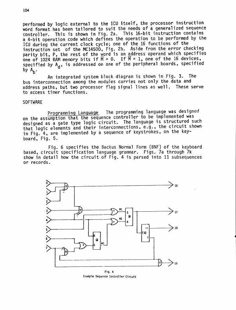
Programming Language The programming language was designed on the assumption that the sequence controller to be implemented was designed as a gate type logic circuit. The language is structured such that logic elements and their interconnections, e.g., the circuit shown · in Fig. 4, are implemented by a sequence of keystrokes, on the key-boa rd, Fig. 5.
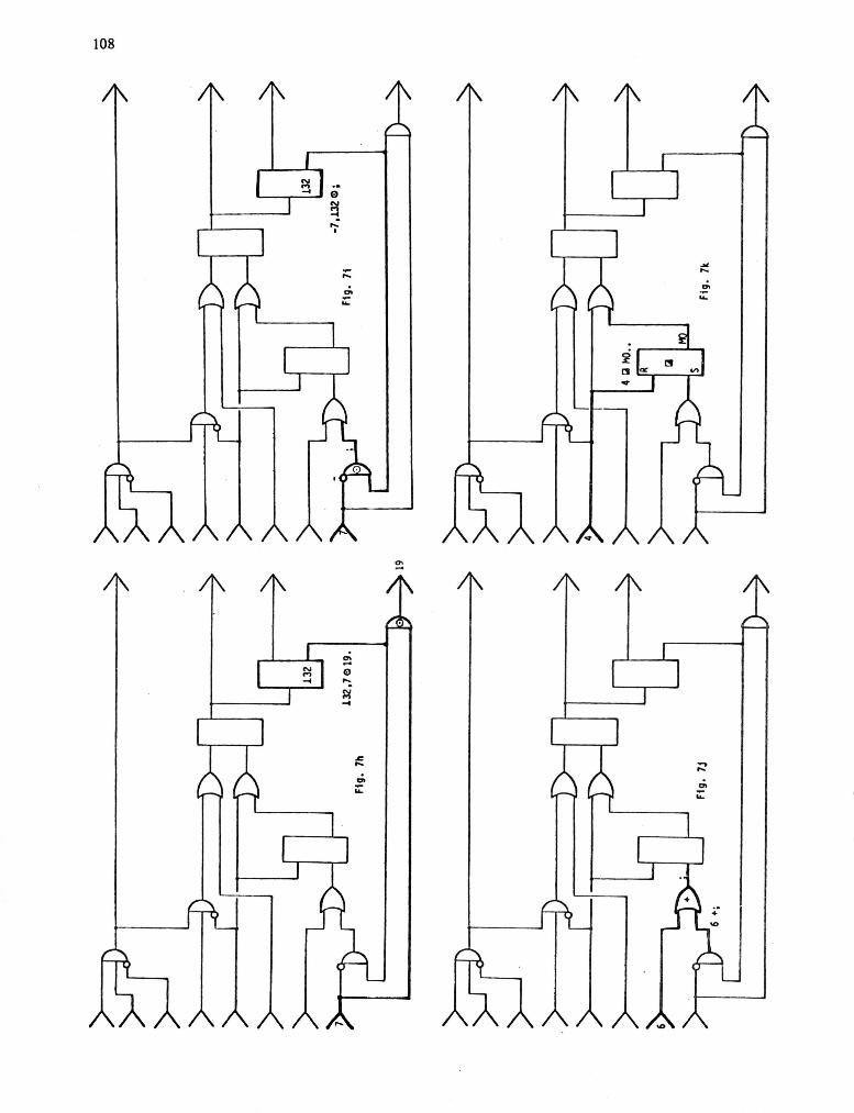
Fig. 6 specifies the Backus Normal Form (BNF) of the keyboard based, circuit specification language grammar. Figs. 7a through 7k show in detail how the circuit of Fig. 4 is parsed into 11 subsequences or records.
~T---------------------------------~16
S 17 till
R
-i 18 32
J. ~
S HO
}-~19 ~----------------------------------~
Fig. 4 Example Sequence Controller Circuit

T ~
1 M
0-9
t +
< RECALL OPERAND ,. :: • ;
~J ~ I ~I T
'--=-' '==-'
7 I I 8 I
~ 5 i 1 ~ >-"
, 0 ,
Description
R-S nip-nop And-Gate Or-Gate
~J J -=J ~
9 I = '-----'
6 i t .-J
~ ~ ; I .
'===:!
Negate signal Input starts timer Output true if timing Output true if timer expired Temporary storage in RAM Assign signal unconditionally Signal/function enumerators Input signal separator . Store/recall previous result for next input operand End of line/enter Delete to previous end of line Delete previous symbol
Fig. 5
Programming Keyboard
< OPER{ND ,. :: • 01112131415161718191< OPERAND ,.< OPERAND ,.
< OPERATOR" :: • Qlel+ITH 11= < TERN" :: • < OPERAND ", < OP~RAND ,. 1-< OPERAND ,. 1 H< OPERAND ,. 1 < OPERAND ", < TERN ,.
< EXPRESSION ,. :: • < TERN >< OPERATOR > 1 ; < TERN >< OPERATOR ,.
< INSTRUCTION > :: • < EXPRESSION >< OPERAND ". 1 < EXPRESSION ,.; 1 < EXPRESSION >H< OPERAND ".1 < EXPRESSION >< OPER{ND ,.;
< PROCEDURE > : : • < INSTRUCTION >.1 < INSTRUCTION >< INSTRUCTION >.
Fig. 6
B N F Grammar of Keystroke language
105
Note that multiple input operands are separated by (J) and records are terminated by (.). A record is defined by a sequence which results in an output. There are four types of record output:-
1. A field output connected to the customer's equipment, 2. An output which starts a timer, 3. An output which, though not assigned to the field or to a
timer, will implicitly constitute the first input in the next record and
4. An output, such as 3. above, which cannot logically be used in the next record and hence must be stored temporarily so that it may be referenced explicitly, later, when it is required as an input.

-Sample Program
~ )16 0 0-
1 0,1.,-2016. 0,1.-2816.
;3,-4 e ; 5+M1·
4 , MO +M 2 .
M1,M2 !;jI17.
; T32 .
-<32=18.
132,7019. -7,1320;
/ I I '\---J fig. 71
6+;
4 ~MO •..
;3,-40; 5+Hl.
fig. 7b Fig. 7e

..... ... 107
108

109
A record closed with a (.) must have an explicit output such as:-1. Field output:- ( .•• 17.), 2. Start timer:- ( .•• T32.) or 3. Temporarily as si g'ned to memory: - ( ... M1.).
If not, it will be lost unless recalled ,by an initial, opening (j) in the next record. Conversely, a record closed with a (.) will regenerate the implied output as the implicit, first operand of the next record. Proper use of (j) will enhance the object program by inhibiting the generation of extra LD and/or ST0 instructions which would inevitably result if the output, and its use as a subsequent input, were explicitly specified. E.g., the sequence:-
0) 1)-2016. j 3)-40 j
saves the extra LD which would be generated by the second record of the following, logically identical, explicit sequence:-
0) 1)-2016. 16) 3)-4@ j
Fig. 8
Compiler Flow Chart
N
N
Fig. 11
Flow Sheet Controller Reprpsentatlon
110
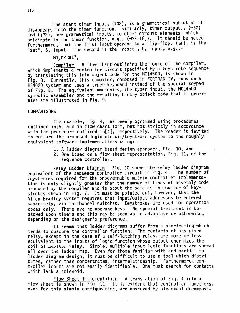
The start timer input, (T32), is a grammatical output which disappears into the timer function. Similarly, timer outputs, {~32} and {132}, are grammatical inputs, to other circuit elements, which originate in the timer function, e.g., {-i32=18,}. It should be not ec, furthermore, that the first input operand to a flip-flop, (IjiI), is the "set", S, input. The second is the "reset", R, input, e.g.:-
M 1.1 M2 t;i 17 , Compiler A flow chart outlining the logic of the compiler,
which implements a controller circuit specified by a k~ystroke ~equence by translating this into object code for the MC14500, 1S shown 1n Fig. 8. Currently, this compiler, composed in FORTRAN IV, runs on a HS4020 system and uses a typer keyboard instead of the special keypad of Fig. 5. The equivalent mnemonics, the typer input, the MC14500 symbolic assembler and the resulting binary object code that it generates are illustrated in Fig. 9.
COMPARISONS
The example, Fig. 4, has been programmed using procedures outlined in[5] and in flow :chart form, but not strictly in accordance with the procedure outlined in[4], respectively. The reader is invited to compare the proposed logic circuit/keystroke system to the roughly equivalent software implementations using:-
1. A ladder diagram based design approach, Fig. 10, and 2. One based on a flow sheet representation, Fig. 11, of the
sequence controller.
Relay Ladder Diagram Fig. 10 shows the relay ladder diagram equivalent of the sequence controller circuit in Fig. 4. The number of keystrokes required for the programmable matrix controller implementation is only slightly greater than the number of lines of assembly code produced by the compiler and is about the same as the number of keystrokes shown in Fig. 7. It must be pointed out, however, that the Allen-Bradley system requires that input/output addresses be entered separately, via thumbwheel switches. Keystrokes are used for operation codes only. There are no operand keys. No special treatment is bestowed upon timers and this may be seen as an advantage or otherwise, depending on the designer's preference.
It seems that ladder diagrams suffer from a shortcoming which tends to obscure the controller function. The contacts of any given relay, except in the case of a self-latching relay, are more or less equivalent to the inputs of logic function whose output energizes the coil of another relay. Simple, multiple input logic functions are spread all over the ladder map. Even for those familiar with and partial to ladder diagram design, it must be difficult to use a tool which distributes, rather than concentrates, interrelationship. Furthermore, controller inputs are not easily identifiable. One must search for contacts which lack a solenoid.
Flow Sheet Implementation A translation of Fig. 4 into a flow sheet is shown in Fig. 11. It is evident that controller functions, even for this simple configuration, are obscured by piecemeal decomposi-

111
tion into auxiliary fragments. In this regard it was not obvious from
descriptions given in[4] how a "Versatyme" controller handles a timer
function if it is required to check timer status, i.e., (~) or (1).
EQUIVALENT MNEMONICS
Teletype Keyboard
A o X B T E , M
(carriage return) F L >
Teletype Keyboard Input
MI4500 USER? 10106 01 11 X2AI6 MI 31 X4AM 501..1 41 L00L2 LIIL2FI7 MB32 T32> 18 £3217 A 19
Programming Keyboa rd
® +
T ~
1
I
(.;i M =
Fi g. 9
Using the Compiler
X7I E32AM 6CM
binary
Compiler Output
hexadecimal assembler
101 000 0 0 10111000 000 1 0 1 0 0 ~Ot10l00
tAgglt88 00111100 0100 100 01011100 1 t) t) .) () 0 0 0
~ ? ~: t t A 8 8 tOt.lt)OOOO
§OQIOOOO 1 (I 1 0 f) ° 8 1 (10000
1 0 tJ I) 1 tJ 0 0 0001100
11110000 00011100 1 t' t) (I 0 1 0 0 o ° 0 (I 0 000 o t' 0) 1 1 1 0 0 00110100 1 (I 'J (I 1 1 0 0 00101100 OO()VOOOO 00110100 01011100 o 1 0 1 0 0 0 0 0lll(II00 8 1 000 1 0 0 11000000
o 000 0 000 00000000 Ot)(JOOl'OO 00000001 00000018 00t)1000 00000011 o 000 0 100 0000010 1 00000001 000001 yO 000000 0 000000 0 QOOOOOOl 000 I 000 1 00000010 0001t)001 00100t)00 o 0 0 0 000 0 o 0 1 0 0 000 000 1 001 0 o 000 0 0 0 0 o 0 1 0 0 0 0 0 00000111 000 1 001 1 00000111 00000000 00100000 00000110 o 0 0 0 0 000 00000100 o 000 0 000 00000000
AO 00 I:IS 00 14 00 34 01 'le 02 I::C 10 3C 03 'le 04 :se 05 BO 01 le 04 ~ 00 eo 02 10 01 50 II '10 O:i e8 II ~'.. . ~o FO 00 le 20 e4 12 00 00 lC 20 34 07 BC 13 2C 0 ·' 00 00 ~4 20 _·e 06 :::'0 00 48 04 B8 00 eo 00
lE'" OION Lll ANlJ ANOC S10 ANLI ANlJC OR 5TO L[) Of< STO LV Of( AI~LlC STO STO NOf'F LD STO NOPO LV AND SltJ LOC NOPO AND OR OR ANDC STO ..IMP
o o
1024 10:iS 1026 10'10 1027 1028 1029
1 1028
2 1
17 2
17 10:56
o 1056 1042
o 1056 1031 1043 1031
o 1056 1030
o
" o o

112
16
---ll 5
---l
17
T32
T32
6
I()
XIC 0 XIC 1 XI0 2 SET 16 XIC 16 XIC 3
3
"
17
4
Z
4 ;r-
7
XIC 32 SET 18 XI0 32 XIC 17 XIC 6 SET 19 XIC 17
16
17
TIMER 32
19
~--.XI0 6 BRT XIC 7 BRT XIC MO XI0 4 SET MO XI0 4
BRTv---~
XIC 5 BRT XIC 17 XI0 4 XIC MO SET 17 XIC 17 SET 32 XI0 32 ~--
XIC Normally Open contact XI0 Normally Closed contact BRT OR SET Energize output
Fig. 10 Programmable Matrix Controller Implementation of Ladder Diagram Design

r-113
CONCLUSION
The development of high level languages and complement ary
system development hardware serves to reinforce the advantages which
microprocessor based sequence controllers enjoy with respect to their
hardwired counterparts. The logic circuit/keystroke approach described
herein should yield a substantial improvement in the productivity of
sequence controller designers; especially those who have some background
in digital logic and assembly language programming.
An impromptu competition, with an interesting outcome, was
held. Five sequence controller designer/programmers set about the im
plementation of a simple circuit based design; one which could be con
veniently evaluated on a commercially available MC14500 Ieu evaluation
kit. The programmers had varying degrees of experience. One used the
preliminary, HS4020 based compiler while the others confined themselves
to hand coding in MC14500 assembly code. The computer assisted imple
mentation tied for first place in terms of the number of instructions
required to correctly emulate the target control circuit. For obvious
reasons, the speed with which the five contestants accomplished their
task will not be compared.
ACKNOWLEDGEMENT
This research is supported by Natural Sciences and Engineering Research Council Canada grant number A4219 and the Bailey Meter Company Limited of Canada.
REFERENCES
[1] Maggioli, V.J., "How to Apply Prograrrmable Controllers", Hydrocarbon
Processing, Vol. 57, No. 12, Dec. 1978, pp. 137-142.
[2] Smith, G.H., "Converting Relay Logic to Software", Machine Design, Vol. 50, No. 19, 24 Aug. 1978, pp. 93-99.
[3] Sanderson; L.B. and Lord, J.C., "Microcomputers Promise Less Stop
More Go", IEEE Spectrum, Vol. 15, No. 11, Nov. 1978, pp.30-32. '
[4] Versatyme System 2 Programmable Controller, Product Specification,
Versatyme Controls Corporation, 1333 Lawrence Expressway, Suite 360, Santa Clara, CA 95051, 1978.
(5] Allen-Bradley Publication SD23, Allen-Bradley Systems Div., Highland Heights, OH 44143, Apr. 1971.
[6] Togino, K. and Fukura, K., "A Computer Route to Ladder Diagrams and
PC Programs", Instrumentation Technology, Vol. 25, No. 5, Sept. 1978, pp. 125-130.
[7] Gregory, V., Dellande, B. et al, "MC14500B Industrial Control Unit
Handbook", Motorola Semiconductor Products Inc., 1977.
[8] Tabach~ick, R.L. and .Zsombor-Murray, P.J., "An Approach to the Imple
mentatlon of Industrlal Sequence Controllers with Standardized Hard
ware.and Firmware", Proc. Cdn. Conf. on Auto. Control, McGill Uni
verslty, Montreal, QU H3A 2K6, 23-25 May 1979. (to be published)


