
CHAPTER 4 60Co GAMMA AND HIGH ENERGY ION IRRADIATION
STUDIES ON 50 GHz SiGe HBTs
4.1. Introduction The 50 GHz SiGe BiCMOS technology was the first in SiGe technologies to enter commercial production at IBM. The first generation SiGe BiCMOS technology integrates 50 GHz SiGe HBT, rf passives (polysilicon and implanted resistors, inductors, metal-insulator metal capacitors), lateral pnp and a higher breakdown (5.3 V) SiGe HBTs [54]. The bandgap-engineered SiGe heterojunction bipolar transistor (SiGe HBT) technology has emerged as a viable candidate for a wide variety of electronic applications operating in extreme environments. The 50 GHz SiGe HBTs have shown built-in multi-Mrad (Si/SiO2) total ionizing dose (TID) tolerance and excellent low temperature performance when compared to Si BJTs [72, 118]. Thus, SiGe HBTs are being considered for upgrade of the front-end readout electronics in the ATLAS detector of the large hadron collider (LHC) [119-121]. The other high end application of SiGe HBTs is in making of radiation hard circuits for space missions [122]. The reliability of SiGe HBTs in extreme environments is particularly important issue for high energy physics experiments, aerospace and various military applications. The accepted best practice is to investigate the reliability of a given device intended to operate in high energy radiation environments by first irradiating the device to very high total dose levels using gamma or proton irradiations. It has been shown that different high energy ion irradiation effects on MOSFETs and transistor show similar degradation to 60Co gamma irradiation even though there is large difference in linear energy transfer [33, 34]. As expected, after heavy ion irradiation (or higher LET radiation), the irradiation time required to reach a particular total dose is much less when compared with gamma or proton irradiation since the heavy ions induce both ionization and displacement damage with large LET when compared to proton or 60Co gamma radiation. Therefore, it is very important to compare the total dose effects of heavy ion and 60Co gamma irradiation on SiGe HBTs with the identical total dose. The heavy ions selected after SRIM simulations were used to irradiate 50 GHz SiGe HBTs. The electrical characteristics like forward and inverse mode Gummel characteristics, excess base current, current gain, neutral base recombination, avalanche multiplication of carriers and output characteristics were measured before and after every irradiation. The electrical characteristics of 60Co gamma and ion irradiated SiGe HBTs are presented and discussed in this chapter.
Chapter 4 66
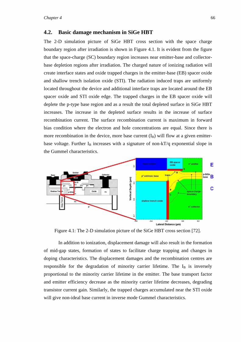
4.2. Basic damage mechanism in SiGe HBT The 2-D simulation picture of SiGe HBT cross section with the space charge boundary region after irradiation is shown in Figure 4.1. It is evident from the figure that the space-charge (SC) boundary region increases near emitter-base and collector-base depletion regions after irradiation. The charged nature of ionizing radiation will create interface states and oxide trapped charges in the emitter-base (EB) spacer oxide and shallow trench isolation oxide (STI). The radiation induced traps are uniformly located throughout the device and additional interface traps are located around the EB spacer oxide and STI oxide edge. The trapped charges in the EB spacer oxide will deplete the p-type base region and as a result the total depleted surface in SiGe HBT increases. The increase in the depleted surface results in the increase of surface recombination current. The surface recombination current is maximum in forward bias condition where the electron and hole concentrations are equal. Since there is more recombination in the device, more base current (IB) will flow at a given emitter- base voltage. Further IB increases with a signature of non-kT/q exponential slope in the Gummel characteristics.
Figure 4.1: The 2-D simulation picture of the SiGe HBT cross section [72].
In addition to ionization, displacement damage will also result in the formation
of mid-gap states, formation of states to facilitate charge trapping and changes in doping characteristics. The displacement damages and the recombination centres are responsible for the degradation of minority carrier lifetime. The IB is inversely proportional to the minority carrier lifetime in the emitter. The base transport factor and emitter efficiency decrease as the minority carrier lifetime decreases, degrading transistor current gain. Similarly, the trapped charges accumulated near the STI oxide will give non-ideal base current in inverse mode Gummel characteristics.

60Co Gamma and High Energy Ion Irradiation Studies on 50 GHz SiGe HBTs 67
The SiGe HBT fabrication is silicon compatible and hence SiGe HBTs
consists of silicon and silicon composites. The different types of dielectrics are used
as emitter base (EB) spacer oxide and shallow trench isolation oxide (STI) depending
on the BiCMOS process. In EB spacer oxide, oxide/nitride composites are used where
as pure SiO2 constitutes STI oxide. When ionizing radiation interacts with SiGe HBT,
a number of electron-hole pairs are produced in different materials of SiGe HBT. In
silicon dioxide (SiO2), one electron-hole pair is produced for every 17 eV of energy
that is deposited in SiO2 [123]. The corresponding energy in silicon to create one
electron-hole pair is 3.6 eV [124]. In silicon nitride (Si3N4), the minimum energy
required to create an electron-hole pair is 6.4 eV.
In silicon, the radiation generated carriers produce transient effects and there
are no long term effects. However in SiO2 long term effects are reported in [125]. A
fraction of electron-hole pairs recombine in oxide in a very short interval of time after
interaction with radiation. The charge yield depends on the electric field and more
carriers survive without recombination in higher electric fields. The surviving
electrons are very mobile in SiO2 and are usually transported out of the oxide in very
short interval of time (in picoseconds). The remaining holes are not very much mobile
and are transported in the oxide by a complicated hopping process. Further, the holes
disperse and transport process typically extends over several orders of magnitude in
time. However some of the holes are trapped in the oxide where they may be stable
for long period of time. Typically in oxides significant hole trapping occurs primarily
near the Si/SiO2 interface [125, 126].
Table 4.1: The bandgap energy, minimum energy required to create an electron-hole (e-h) pair and e-h pair density in different materials of SiGe HBT.
Materials used in SiGe HBT
Bandgap energy, Eg
(eV)
Minimum energy required for e-h pair
creation, Ep (eV)
Density (g/cm3)
e-h pair density generated per rad,
go (pairs/cm3) Silicon 1.11 3.6 2.32 4.0x10¹³
Silicon nitride 5.1 6.4 3.44 3.3x10¹³
Silicon dioxide 8.9 17 2.25 8.1x10¹²

Chapter 4 68
Table 4.1 shows the bandgap energy, minimum energy required to create an electron-hole pair and the electron-hole pair density in different materials of SiGe HBT. The electron-hole pair density is obtained from the product of the material density and the energy deposited per rad divided by Ep. The number of electron hole pair density is more in silicon than silicon dioxide and silicon nitride. In silicon nitride the electron hole pair density is higher than that of silicon dioxide. It is reported that the defects like oxygen vacancy and hydrogen vacancy at or near the Si/SiO2 interface have key roles in determining the defect density of irradiated and stressed oxides [127]. The nitrided oxides are composed of nitrogen-rich region at the interface and a lower concentration of nitrogen in the bulk of the film [128]. In oxide/nitride composites used in semiconductor devices, nitrogen plays an important to improve the trapping properties of the near interfacial oxide in which border traps are found. The suppression of interface-state generation in the nitride/oxides is related to the build-up of nitrogen near the insulator-silicon interface. The radiation induced trapped charges in nitrided oxide readily recombine in very short time when compared to the trapped charges generated in SiO2. Hence the oxide/nitride composite is used in EB spacer oxide of SiGe HBTs. Therefore the radiation hardness of SiGe HBTs has to be measured up to a very high total dose. It is evident from the literature survey that the effects of proton, neutron and 60Co gamma irradiation is well understood up to a total dose of 6 Mrad. It is important and interesting to study the effects of swift heavy ion irradiation on SiGe HBTs before one can use ion irradiation for radiation testing. The objective of this work is to investigate the effects of different high energy ion irradiation on I–V characteristics of 50 GHz SiGe HBTs. The ion irradiation results are compared with 60Co gamma irradiation results and the results are presented in the following sections.
4.3. Results and discussions The 50 GHz SiGe HBTs were exposed to 60Co gamma radiation and different high energy ions such as 50 MeV lithium ions, 75 MeV boron ions and 100 MeV oxygen ions. The SiGe HBTs were irradiated at different total doses from 600 krad to 100 Mrad. The in-situ electrical measurements were carried after exposure to different total doses. The electrical characteristics like forward mode and inverse mode Gummel characteristics, excess base current, current gain, damage constant, neutral base recombination, avalanche multiplication of carriers and output characteristics are presented in the following sections.
60Co Gamma and High Energy Ion Irradiation Studies on 50 GHz SiGe HBTs 69
4.4. The effects of 60Co gamma and high energy ion irradiation on the electrical characteristics of 50GHz SiGe HBTs
The important electrical characteristics of SiGe HBT were studied before and after
irradiation and the results are discussed below.
4.4.1. Forward Gummel characteristics The forward Gummel characteristics represents the variation of collector current (IC)
and base current (IB) in logarithmic scale against linearly increasing emitter-base
voltage (VBE). The forward mode Gummel characteristic is studied to assess the
radiation induced changes in the emitter-base (EB) spacer oxide. Therefore after every
total dose, Gummel characteristic is measured to observe the changes in IB and IC. The
forward mode Gummel characteristics of 60Co gamma, 50 MeV Li3+ ion, 75 MeV B5+
ion and 100 MeV O7+ ion irradiated SiGe HBT with emitter area (AE) of 0.5 x 2.5
μm2 are shown in Figures 4.2 to 4.5. From the figures it can be seen that IB increases
at lower VBE with increase in radiation dose but IC remains the same even after 100
Mrad of total dose. Therefore only pre-rad IC curve is shown for brevity. The radiation
induced generation–recombination (G/R) traps near EB spacer oxide are responsible
for the observed increase in IB. The increase in IB is the result of increased
recombination current in the EB depletion region. The ionizing radiation creates
damage at the periphery of the EB spacer oxide and ion irradiation creates damage
even inside the EB spacer oxide [4, 73, 129]. Figures 4.6 to 4.9 show the post-
irradiation forward mode IB normalised to the un-irradiation IB for SiGe HBTs
exposed to different radiation. From these figures it can be seen that the IB increased
significantly at lower VBE with increase in radiation dose. The characteristic increase
in the low injection IB is mainly due to the phenomenon of radiation induced G/R trap
centres in the EB spacer oxide. The normalized IB increases with increase in linear
energy transfer (LET) of the incident radiation. The LET of the incident radiation
increases significantly for ions of higher atomic number. Therefore, higher LET
radiation create more G/R trapped charges in EB spacer oxide.

Chapter 4 70
0.4 0.6 0.8 1.0 1.21x10⁻¹⁰
1x10⁻⁹
1x10⁻⁸
1x10⁻⁷
1x10⁻⁶
1x10⁻⁵
1x10⁻⁴
1x10⁻³
1x10⁻²
I C, I B (
A)
VBE (V)
5AM SiGe HBTForward Gummel characteristicsAE = 0.5 x 2.5 µm2
Co-60 gamma radiation IB Prerad IC Prerad 600 krad 1 Mrad 3 Mrad 6 Mrad 10 Mrad 30 Mrad 60 Mrad 100 Mrad
Figure 4.2: Forward mode Gummel characteristics of 60Co gamma irradiated SiGe HBT.
0.4 0.6 0.8 1.0 1.21x10⁻¹⁰
1x10⁻⁹
1x10⁻⁸
1x10⁻⁷
1x10⁻⁶
1x10⁻⁵
1x10⁻⁴
1x10⁻³
1x10⁻²
5AM SiGe HBTsForward Gummel CharacteristicsAE = 0.5 x 2.5 µm2
50 MeV Lithium ion
I C, I B
(A)
VBE(V)
IC Prerad IB Prerad 600 krad 1 Mrad 3 Mrad 6 Mrad 10 Mrad 30 Mrad 60 Mrad 100 Mrad
Figure 4.3: Forward mode Gummel characteristics of 50 MeV Li3+ ion irradiated SiGe HBT.
0.4 0.6 0.8 1.0 1.21x10⁻¹⁰
1x10⁻⁹
1x10⁻⁸
1x10⁻⁷
1x10⁻⁶
1x10⁻⁵
1x10⁻⁴
1x10⁻³
1x10⁻²
5AM SiGe HBTForward Gummel characteristicsAE = 0.5 x 2.5 µm2
75 MeV Boron ion Prerad IC Prerad IB 600 krad 1 Mrad 3 Mrad 6 Mrad 10 Mrad 30 Mrad 60 Mrad 100 Mrad
I C, I B (
A)
VBE (V)
Figure 4.4: Forward mode Gummel characteristics of 75 MeV B5+ ion irradiated SiGe HBT.
0.4 0.6 0.8 1.0 1.21x10⁻¹⁰
1x10⁻⁹
1x10⁻⁸
1x10⁻⁷
1x10⁻⁶
1x10⁻⁵
1x10⁻⁴
1x10⁻³
1x10⁻²
5AM SiGe HBTForward Gummel CharacteristicsAE = 0.5 x 2.5 µm2
100 MeV Oxygen ion
VBE (V)
I C, I B (
A)
Prerad IC Prerad IB 3 Mrad 6 Mrad 10 Mrad 30 Mrad 60 Mrad 100 Mrad
Figure 4.5: Forward mode Gummel characteristics of 100 MeV O7+ ion irradiated SiGe HBT.
0.3 0.4 0.5 0.6 0.7 0.8 0.91x100
1x101
1x10²
1x10³
1x10⁴
Co-60 gamma radiationForward mode normalised IB
I Bpo
st /
I Bpr
e
VBE (V)
5AM SiGe HBTAE = 0. 5 x 2.5 µm2
600 krad 1 Mrad 3 Mrad 6 Mrad 10 Mrad 30 Mrad 60 Mrad 100 Mrad
Figure 4.6: Forward mode normalised base current (IBPost/IBPre) of 60Co gamma irradiated SiGe HBT.
0.5 0.6 0.7 0.8 0.91x100
1x101
1x10²
1x10³
1x10⁴
50 MeV Lithium ionForward mode normalised IB
I Bpo
st /
I Bpr
e
VBE (V)
5AM SiGe HBTAE = 0. 5 x 2.5 µm2
600 krad 1 Mrad 3 Mrad 6 Mrad 10 Mrad 30 Mrad 60 Mrad 100 Mrad
Figure 4.7: Forward mode normalised base current (IBPost/IBPre) of 50 MeV Li3+ ion irradiated SiGe HBT.

60Co Gamma and High Energy Ion Irradiation Studies on 50 GHz SiGe HBTs 71
0.3 0.4 0.5 0.6 0.7 0.8 0.91x10⁻¹
1x100
1x101
1x10²
1x10³
1x10⁴
75 MeV Boron ionForward mode normalised IB
I Bpos
t / I Bp
re
VBE (V)
5AM SiGe HBTAE = 0. 5 x 2.5 µm2
600 krad 1 Mrad 3 Mrad 6 Mrad 10 Mrad 30 Mrad 60 Mrad 100 Mrad
Figure 4.8: Forward mode normalised base current (IBPost/IBPre) of 75 MeV B5+ ion irradiated SiGe HBT.
0.3 0.4 0.5 0.6 0.7 0.8 0.91x100
1x101
1x10²
1x10³
1x10⁴
100 MeV Oxygen ionForward mode normalised IB
VBE (V)
I Bpos
t / I Bp
re
5AM SiGe HBTAE = 0. 5 x 2.5 µm2
3 Mrad 6 Mrad 10 Mrad 30 Mrad 60 Mrad 100 Mrad
Figure 4.9: Forward mode normalised base current (IBPost/IBPre) of 100 MeV O7+ ion irradiated SiGe HBT.
1 10 1000
2x10⁻⁸
4x10⁻⁸
6x10⁻⁸
8x10⁻⁸
1x10⁻⁷
1x10⁻⁷
5AM SiGe HBTForward mode excess base currentAE = 0.5 x 2.5 µm2
@VBE = 0.65 V∆IB = IBpost - IBpre
Exce
ss b
ase
curr
ent (
A)
Total dose (Mrad(Si))
Co-60 Gamma 50 MeV Lithium 75 MeV Boron 100 MeV Oxygen
Prerad
Figure 4.10: The variation in forward mode excess base current at VBE = 0.65 V after gamma and ion irradiation.
1 10 1000
20
40
60
80
100
Co-60 Gamma 50 MeV Lithium 75 MeV Boron 100 MeV Oxygen
(∆Ι Β/Ι
Β) x
100
Total dose (Mrad(Si))
5AM SiGe HBTAE = 0.5 x 2.5 µm2
Forward mode normalised IB@ VBE = 0.65 V
Prerad
Figure 4.11: The variation in forward mode excess base current normalised to 100 for gamma and ion irradiated SiGe HBT.
The increase in IB for forward mode Gummel characteristics (IBpost) is measured at VBE = 0.65 V for various total doses and VBE
= 0.65 V is chosen to avoid high injection effects where large carrier densities severely diminish the G/R effects of radiation induced traps. The bias levels much lower than VBE
= 0.65 V result in much smaller currents and less reliable measurements of ΔIB. The forward mode excess base current (ΔIB = IBpost – IBpre) is plotted versus total dose for SiGe HBTs irradiated with gamma and ion and is shown in figure 4.10. The forward mode
normalised excess base current �𝚫𝚫𝐈𝐈𝐁𝐁𝐈𝐈𝐁𝐁𝐱𝐱𝐱𝐱𝐱𝐱𝐱𝐱� for gamma and ion irradiated SiGe HBTs
is shown in Figure 4.11. From the figures it is clear that the forward mode ΔIB is found to increase around two orders of magnitude after gamma and ion irradiation. The increase in forward mode ΔIB is more for ion irradiated SiGe HBT when

Chapter 4 72
compared to gamma irradiated SiGe HBT. Therefore more G/R trapped charges are created in EB spacer oxide after ion irradiation when compared to gamma irradiation. In SiGe HBTs, the EB spacer oxide is an oxide/nitride composite [4]. The effects of nitrogen near the insulator/silicon improves the radiation hardening by undergoing recombination in short time and thereby leaving fewer radiation induced G/R traps [130]. The resistance offered by the oxide/nitride composite to space charge build-up is the result of efficient recombination centers in the material and balanced densities of deep hole and electron traps [131]. Therefore the EB spacer oxide is more immune to the formation of long term defects due to gamma irradiation.
4.4.2. Inverse Gummel characteristics The radiation damage in shallow trench isolation (STI) oxide is studied by swapping
emitter and collector terminals while taking Gummel measurements and such a
measurement is called inverse mode Gummel characteristics. In other words, VBE is
actually VBC in inverse mode Gummel characteristics. The inverse mode Gummel
characteristics of 60Co gamma, 50 MeV Li3+ ion, 75 MeV B5+ ion and 100 MeV O7+
ion irradiated SiGe HBTs are shown in Figures 4.12 to 4.15 respectively. The inverse
mode Gummel plots show the inverse mode I-V characteristics of SiGe HBT with
emitter area (AE) 0.5 x 2.5 μm2, irradiated up to a total dose of 100 Mrad (Si). From
the figures it is evident that as the ion and gamma dose increases, the IB increases at
lower VBE. In this case, the radiation induced traps in the STI oxide now act as G/R
trap centres in the inverse EB junction (i.e., collector-base junction). These G/R traps
increase the IB by generation-recombination process and hence IB increases at lower
VBE. The radiation induced trapped charges are created along the periphery of STI
oxide and hence the space charge region in the CB junction increases after irradiation
[70]. The post-irradiation inverse mode IB normalized to the pre-irradiation IB for 60Co
gamma, 50 MeV Li3+, 75 MeV B5+ and 100 MeV O7+ ion irradiated SiGe HBTs are
shown in Figures 4.16 to 4.19 respectively. From the figures it is evident that the
normalized IB increases at lower VBE with increase in radiation total dose. The
normalised IB increases with increase in the LET of the incident radiation. The
increase in normalised IB is very less for Li3+ ion irradiated SiGe HBT when
compared to the normalised IB of SiGe HBTs irradiated with other radiations. The
increase in inverse mode normalized IB is around 2 to 3 orders of magnitude for 60Co
gamma, B5+ ion and O7+ ion irradiated SiGe HBTs.

60Co Gamma and High Energy Ion Irradiation Studies on 50 GHz SiGe HBTs 73
0.4 0.6 0.8 1.0 1.21x10⁻¹⁰
1x10⁻⁹
1x10⁻⁸
1x10⁻⁷
1x10⁻⁶
1x10⁻⁵
1x10⁻⁴
1x10⁻³
1x10⁻²
VBE (V)
I C, I B (
A)5AM SiGe HBTAE = 0.5 x 2.5 µm2
Inverse Gummel characteristicsCo-60 gamma radiation
IC Prerad IB Prerad 600 krad 1 Mrad 3 Mrad 6 Mrad 10 Mrad 30 Mrad 60 Mrad 100 Mrad
Figure 4.12: Inverse mode Gummel characteristics of 60Co gamma irradiated SiGe HBT.
0.4 0.6 0.8 1.0 1.21x10⁻¹⁰
1x10⁻⁹
1x10⁻⁸
1x10⁻⁷
1x10⁻⁶
1x10⁻⁵
1x10⁻⁴
1x10⁻³
1x10⁻²
5AM SiGe HBTsInverse Gummel CharacteristicsAE = 0.5 x 2.5 µm2
50 MeV Lithium ion
I C, I B
(A)
VBE (V)
IC Prerad IB Prerad 600 krad 1 Mrad 3 Mrad 6 Mrad 10 Mrad 30 Mrad 60 Mrad 100 Mrad
Figure 4.13: Inverse mode Gummel characteristics of 50 MeV Li3+ ion irradiated SiGe HBT.
0.4 0.6 0.8 1.0 1.21x10⁻¹⁰
1x10⁻⁹
1x10⁻⁸
1x10⁻⁷
1x10⁻⁶
1x10⁻⁵
1x10⁻⁴
1x10⁻³
1x10⁻²
5AM SiGe HBTInverse Gummel characteristicsAE = 0.5 x 2.5 µm2
75 MeV Boron ion IC Prerad IB Prerad 600 krad 1 Mrad 3 Mrad 6 Mrad 10 Mrad 30 Mrad 60 Mrad 100 Mrad
I C, I B (
A)
VBE (V)
Figure 4.14: Inverse mode Gummel characteristics of 75 MeV B5+ ion irradiated SiGe HBT.
0.4 0.6 0.8 1.0 1.21x10⁻¹⁰
1x10⁻⁹
1x10⁻⁸
1x10⁻⁷
1x10⁻⁶
1x10⁻⁵
1x10⁻⁴
1x10⁻³
1x10⁻²
5AM SiGe HBTInverse Gummel CharacteristicsAE = 0.5 x 2.5 µm2
100 MeV Oxygen ion
IC Prerad IB Prerad 3 Mrad 6 Mrad 10 Mrad 30 Mrad 60 Mrad 100 Mrad
I C, I B (
A)
VBE (V)
Figure 4.15: Inverse mode Gummel characteristics of 100 MeV O7+ ion irradiated SiGe HBT.
0.3 0.4 0.5 0.6 0.7 0.8 0.91x100
1x101
1x10²
1x10³
1x10⁴
Co-60 gamma radiationInverse mode normalised IB
I Bpo
st /
I Bpr
e
VBE (V)
5AM SiGe HBTAE = 0. 5 x 2.5 µm2
600 krad 1 Mrad 3 Mrad 6 Mrad 10 Mrad 30 Mrad 60 Mrad 100 Mrad
Figure 4.16: Inverse mode normalised base current (IBPost/IBPre) of 60Co gamma irradiated SiGe HBT.
0.5 0.6 0.7 0.8 0.91x100
1x101
1x10²
VBE (V)
I Bpos
t / I Bp
re
50 MeV Lithium ionInverse mode normalised IB
5AM SiGe HBTAE = 0. 5 x 2.5 µm2
600 krad 1 Mrad 3 Mrad 6 Mrad 10 Mrad 30 Mrad 60 Mrad 100 Mrad
Figure 4.17: Inverse mode normalised base current (IBPost/IBPre) of 50 MeV Li3+ ion irradiated SiGe HBT.

Chapter 4 74
0.4 0.5 0.6 0.7 0.81x100
1x101
1x10²
1x10³
1x10⁴
75 MeV Boron ionInverse mode normalised IB
I Bpo
st /
I Bpr
e
VBE (V)
5AM SiGe HBTAE = 0. 5 x 2.5 µm2
600 krad 1 Mrad 3 Mrad 6 Mrad 10 Mrad 30 Mrad 60 Mrad 100 Mrad
Figure 4.18: Inverse mode normalised base current (IBPost/IBPre) of 75 MeV B5+ ion irradiated SiGe HBT.
0.3 0.4 0.5 0.6 0.7 0.8 0.91x100
1x101
1x10²
1x10³
I Bpos
t / I Bp
re
VBE (V)
100 MeV Oxygen ionInverse mode normalised IB
5AM SiGe HBTAE = 0. 5 x 2.5 µm2
3 Mrad 6 Mrad 10 Mrad 30 Mrad 60 Mrad 100 Mrad
Figure 4.19: Inverse mode normalised base current (IBPost/IBPre) of 100 MeV O7+ ion irradiated SiGe HBT.
The inverse mode excess base current (ΔIB = IBpost – IBpre) measured at VBE =
0.65 V is plotted versus total dose for gamma and ion irradiated SiGe HBTs and is
shown in Figure 4.20. It can be seen that, the increase in inverse mode ΔIB is more for
gamma irradiated SiGe HBT when compared to ion irradiated SiGe HBT up to 10
Mrad of total dose. Therefore more number of G/R trapped charges are created in
shallow trench isolation (STI) oxide after gamma irradiation when compared to high
energy ion irradiation. In the previous section (4.4.1), it was observed that EB spacer
oxide is more radiation tolerant to ionizing radiation, but susceptible to damages after
high energy ion irradiation. Therefore the radiation response of EB spacer oxide is
different from that of STI oxide for different radiations. This different behavior of EB
spacer oxide and STI oxide to different radiation is mainly due to the EB spacer oxide
is oxide/nitride composite whereas the STI oxide is purely silicon dioxide (SiO2). At
lower total doses (up to 10 Mrad), SiO2 is more susceptible to damage for gamma
radiation. Above 10 Mrad of total dose the increase in inverse mode ΔIB is more for
ion irradiated SiGe HBT when compared to gamma irradiated SiGe HBT. Therefore
high energy ions induce more trapped charges above 10 Mrad when compared to
gamma radiation. The inverse mode normalised excess base current �𝚫𝚫𝐈𝐈𝐁𝐁𝐈𝐈𝐁𝐁𝐱𝐱𝐱𝐱𝐱𝐱𝐱𝐱� for
gamma and ion irradiated SiGe HBTs are shown in Figure 4.21. The inverse mode
normalized ΔIB is less for 50 MeV Li3+ ion irradiated SiGe HBT when compared to
other radiations, which is unexpected. After 100 Mrad of total dose the inverse mode
normalized ΔIB is same for 60Co gamma, 75 MeV B5+ and 100 MeV O7+ ion
irradiated SiGe HBTs.

60Co Gamma and High Energy Ion Irradiation Studies on 50 GHz SiGe HBTs 75
1 10 1000
1x10⁻⁷
2x10⁻⁷
3x10⁻⁷
4x10⁻⁷
5x10⁻⁷
6x10⁻⁷
5AM SiGe HBTAE = 0.5 x 2.5 µm2
Inverse mode excess base current@ VBE = 0.65 V
Exce
ss b
ase
curr
ent (
A)
Total dose (Mrad(Si))
Co-60 Gamma 50 MeV Lithium 75 MeV Boron 100 MeV Oxygen
Prerad
Figure 4.20: The variation of inverse mode excess base current at VBE = 0.65 V after gamma and ion irradiation.
1 10 1000
20
40
60
80
1005AM SiGe HBTAE = 0.5 x 2.5 µm2
Inverse mode normalised IB@ VBE = 0.65 V
Co-60 Gamma 50 MeV Lithium 75 MeV Boron 100 MeV Oxygen
(∆Ι Β/Ι
Β) x
100
Total dose (Mrad(Si))Prerad
Figure 4.21: The variation of inverse mode excess base current normalised to 100 for gamma and ion irradiated SiGe HBT.
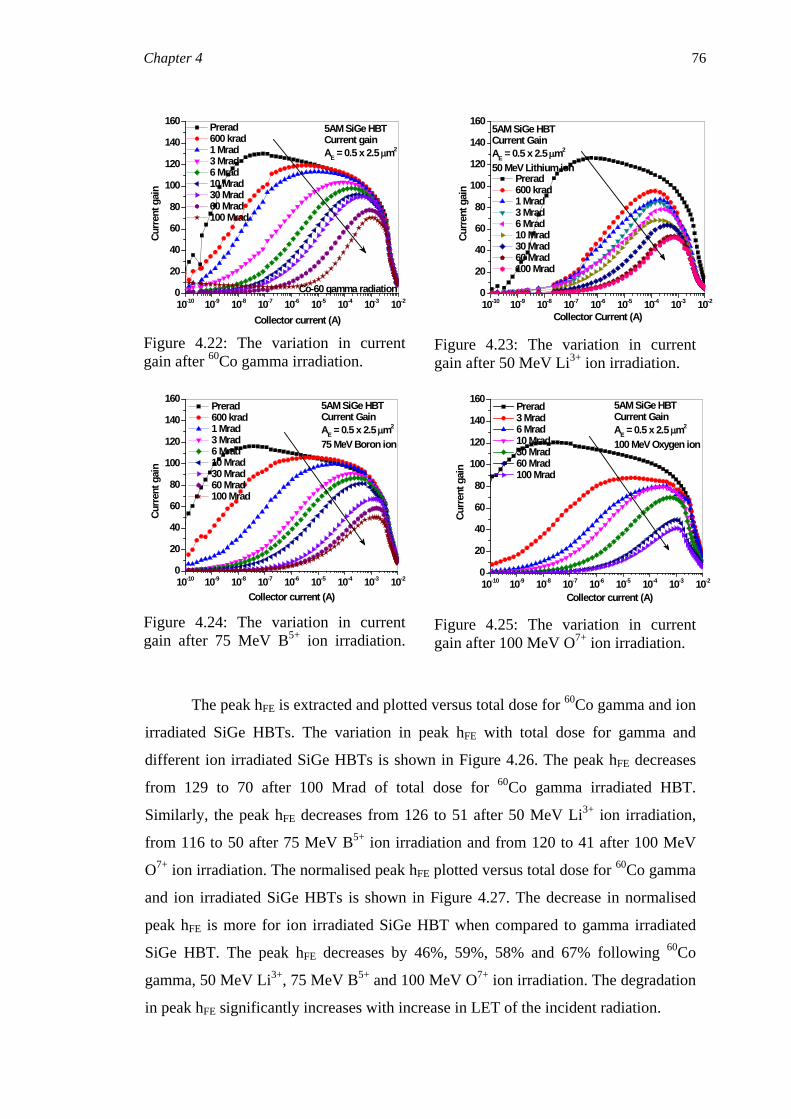
4.4.3. Current gain The DC current gain (hFE = IC / IB) is extracted from the forward Gummel
characteristics. The current gain of gamma and ion irradiated SiGe HBTs with emitter
area 0.5 x 2.5 µm2 are shown in Figures 4.22 to 4.25. From the figures it can be seen
that hFE decreases with increase in radiation total dose. The decrease in hFE is
consistent with the increase in the forward mode ΔIB for gamma and ion irradiated
SiGe HBTs. The peak hFE decreases and shifts towards to higher IC or higher VBE with
increasing radiation total dose. The shift in peak hFE is due to non-ideal increase in IB
at lower VBE. The hFE degradation in SiGe HBTs occurs in two ways: one is bulk
degradation and the other is ionization of the oxide/nitride composite. The bulk
degradation occurs due to atomic displacement in the bulk of the transistor. The
transfer of sufficiently large amount of energy to transistor, the silicon atoms can be
ejected from its location, leaving a vacancy or defect. This displacement damage is a
bulk effect deep inside the transistor structure. These defects act as G/R centers in the
transistor and reduce the minority carrier lifetime and therefore the IB increases and
hFE decreases. The traps with the energies near the middle of the silicon bandgap are
the most effective in reducing the minority carrier lifetime. The decrease in minority
carrier lifetime is the dominant mechanism for hFE degradation in addition to G/R
centers in the EB spacer oxide.
Chapter 4 76
10-10 10-9 10-8 10-7 10-6 10-5 10-4 10-3 10-20
20
40
60
80
100
120
140
160
Co-60 gamma radiation
5AM SiGe HBTCurrent gainAE = 0.5 x 2.5 µm2
Prerad 600 krad 1 Mrad 3 Mrad 6 Mrad 10 Mrad 30 Mrad 60 Mrad 100 Mrad
Curr
ent g
ain
Collector current (A)
Figure 4.22: The variation in current gain after 60Co gamma irradiation.
10-10 10-9 10-8 10-7 10-6 10-5 10-4 10-3 10-20
20
40
60
80
100
120
140
1605AM SiGe HBTCurrent GainAE = 0.5 x 2.5 µm2
50 MeV Lithium ion
Curre
nt g
ain
Collector Current (A)
Prerad 600 krad 1 Mrad 3 Mrad 6 Mrad 10 Mrad 30 Mrad 60 Mrad 100 Mrad
Figure 4.23: The variation in current gain after 50 MeV Li3+ ion irradiation.
10-10 10-9 10-8 10-7 10-6 10-5 10-4 10-3 10-20
20
40
60
80
100
120
140
160 5AM SiGe HBTCurrent GainAE = 0.5 x 2.5 µm2
75 MeV Boron ion
Prerad 600 krad 1 Mrad 3 Mrad 6 Mrad 10 Mrad 30 Mrad 60 Mrad 100 Mrad
Curr
ent g
ain
Collector current (A)
Figure 4.24: The variation in current gain after 75 MeV B5+ ion irradiation.
10-10 10-9 10-8 10-7 10-6 10-5 10-4 10-3 10-20
20
40
60
80
100
120
140
160 5AM SiGe HBTCurrent GainAE = 0.5 x 2.5 µm2
100 MeV Oxygen ion
Prerad 3 Mrad 6 Mrad 10 Mrad 30 Mrad 60 Mrad 100 Mrad
Curr
ent g
ain
Collector current (A)
Figure 4.25: The variation in current gain after 100 MeV O7+ ion irradiation.
The peak hFE is extracted and plotted versus total dose for 60Co gamma and ion
irradiated SiGe HBTs. The variation in peak hFE with total dose for gamma and
different ion irradiated SiGe HBTs is shown in Figure 4.26. The peak hFE decreases
from 129 to 70 after 100 Mrad of total dose for 60Co gamma irradiated HBT.
Similarly, the peak hFE decreases from 126 to 51 after 50 MeV Li3+ ion irradiation,
from 116 to 50 after 75 MeV B5+ ion irradiation and from 120 to 41 after 100 MeV
O7+ ion irradiation. The normalised peak hFE plotted versus total dose for 60Co gamma
and ion irradiated SiGe HBTs is shown in Figure 4.27. The decrease in normalised
peak hFE is more for ion irradiated SiGe HBT when compared to gamma irradiated
SiGe HBT. The peak hFE decreases by 46%, 59%, 58% and 67% following 60Co
gamma, 50 MeV Li3+, 75 MeV B5+ and 100 MeV O7+ ion irradiation. The degradation
in peak hFE significantly increases with increase in LET of the incident radiation.

60Co Gamma and High Energy Ion Irradiation Studies on 50 GHz SiGe HBTs 77
1 10 10020
40
60
80
100
120
140
Peak
cur
rent
gai
n
Total dose (Mrad(Si))
5AM SiGe HBTPeak current gainAE = 0.5 x 2.5 µm2
Co-60 Gamma 50 MeV Lithium 75 MeV Boron 100 MeV Oxygen
Prerad
Figure 4.26: The peak current gain versus total dose for gamma and ion irradiated SiGe HBTs.
1 10 1000
20
40
60
80
100
Total dose (Mrad(Si))
5 AM SiGe HBTNormalised Peak Current GainAE= 0.5 x 2.5 µm2
Co-60 Gamma 50 MeV Lithium 75 MeV Boron 100 MeV Oxygen
Norm
alis
ed p
eak
curr
ent g
ain
Prerad
Figure 4.27: The current gain normalised to pre irradiation value [(hFEpost/hFEpre)x100] versus total dose for gamma and ion irradiated SiGe HBTs.
1 10 1001x10-4
1x10⁻³
1x10⁻²
Co-60 Gamma 50 MeV Lithium 75 MeV Boron 100 MeV Oxygen
1/h FE
(0) -
1/h
FE(φ
)
Total dose (Mrad(Si))Prerad
Figure 4.28: The ∆ � 𝐱𝐱
𝐡𝐡𝐅𝐅𝐅𝐅� versus total dose for
gamma and ion irradiated SiGe HBTs.
The Messenger–Spratt equation is given by [132];
� 𝐱𝐱𝐡𝐡𝐅𝐅𝐅𝐅(𝛗𝛗)
− 𝐱𝐱𝐡𝐡𝐅𝐅𝐅𝐅(𝐱𝐱)
� = ∆ � 𝐱𝐱𝐡𝐡𝐅𝐅𝐅𝐅� = 𝐊𝐊𝛗𝛗 → 4.1
where, 𝐱𝐱𝐡𝐡𝐅𝐅𝐅𝐅(𝛗𝛗)
is the reciprocal of current gain for a given dose, 𝐱𝐱𝐡𝐡𝐅𝐅𝐅𝐅(𝐱𝐱)
is the reciprocal
of pre-rad current gain, K is composite damage constant and φ is the particular given
dose. The above equation is used to calculate the damage constant due to irradiation.
The variation of ∆ � 𝐱𝐱𝐡𝐡𝐅𝐅𝐅𝐅� versus total dose is shown in Figure 4.28. The damage
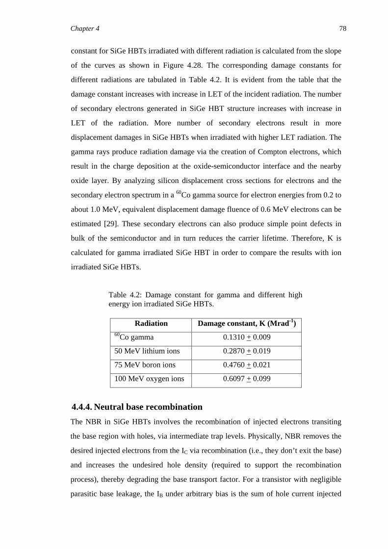
Chapter 4 78
constant for SiGe HBTs irradiated with different radiation is calculated from the slope
of the curves as shown in Figure 4.28. The corresponding damage constants for
different radiations are tabulated in Table 4.2. It is evident from the table that the
damage constant increases with increase in LET of the incident radiation. The number
of secondary electrons generated in SiGe HBT structure increases with increase in
LET of the radiation. More number of secondary electrons result in more
displacement damages in SiGe HBTs when irradiated with higher LET radiation. The
gamma rays produce radiation damage via the creation of Compton electrons, which
result in the charge deposition at the oxide-semiconductor interface and the nearby
oxide layer. By analyzing silicon displacement cross sections for electrons and the
secondary electron spectrum in a 60Co gamma source for electron energies from 0.2 to
about 1.0 MeV, equivalent displacement damage fluence of 0.6 MeV electrons can be
estimated [29]. These secondary electrons can also produce simple point defects in
bulk of the semiconductor and in turn reduces the carrier lifetime. Therefore, K is
calculated for gamma irradiated SiGe HBT in order to compare the results with ion
irradiated SiGe HBTs.
Table 4.2: Damage constant for gamma and different high energy ion irradiated SiGe HBTs.
Radiation Damage constant, K (Mrad-1)
60Co gamma 0.1310 + 0.009
50 MeV lithium ions 0.2870 + 0.019
75 MeV boron ions 0.4760 + 0.021
100 MeV oxygen ions 0.6097 + 0.099
4.4.4. Neutral base recombination The NBR in SiGe HBTs involves the recombination of injected electrons transiting
the base region with holes, via intermediate trap levels. Physically, NBR removes the
desired injected electrons from the IC via recombination (i.e., they don’t exit the base)
and increases the undesired hole density (required to support the recombination
process), thereby degrading the base transport factor. For a transistor with negligible
parasitic base leakage, the IB under arbitrary bias is the sum of hole current injected
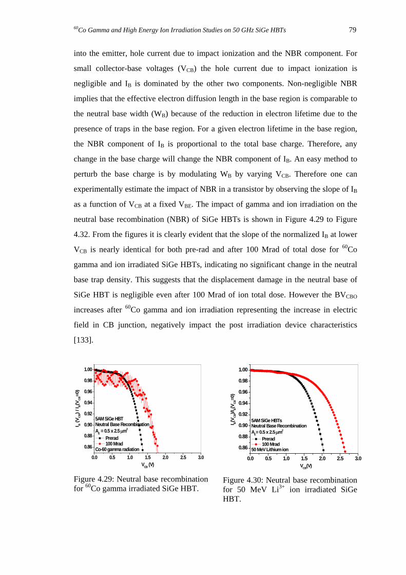
60Co Gamma and High Energy Ion Irradiation Studies on 50 GHz SiGe HBTs 79
into the emitter, hole current due to impact ionization and the NBR component. For
small collector-base voltages (VCB) the hole current due to impact ionization is
negligible and IB is dominated by the other two components. Non-negligible NBR
implies that the effective electron diffusion length in the base region is comparable to
the neutral base width (WB) because of the reduction in electron lifetime due to the
presence of traps in the base region. For a given electron lifetime in the base region,
the NBR component of IB is proportional to the total base charge. Therefore, any
change in the base charge will change the NBR component of IB. An easy method to
perturb the base charge is by modulating WB by varying VCB. Therefore one can
experimentally estimate the impact of NBR in a transistor by observing the slope of IB
as a function of VCB at a fixed VBE. The impact of gamma and ion irradiation on the
neutral base recombination (NBR) of SiGe HBTs is shown in Figure 4.29 to Figure
4.32. From the figures it is clearly evident that the slope of the normalized IB at lower
VCB is nearly identical for both pre-rad and after 100 Mrad of total dose for 60Co
gamma and ion irradiated SiGe HBTs, indicating no significant change in the neutral
base trap density. This suggests that the displacement damage in the neutral base of
SiGe HBT is negligible even after 100 Mrad of ion total dose. However the BVCBO
increases after 60Co gamma and ion irradiation representing the increase in electric
field in CB junction, negatively impact the post irradiation device characteristics
[133].
0.0 0.5 1.0 1.5 2.0 2.5 3.0
0.86
0.88
0.90
0.92
0.94
0.96
0.98
1.00
I B (V
CB) /
I B(V
CB=0
)
VCB (V)
5AM SiGe HBTNeutral Base RecombinationAE = 0.5 x 2.5 µm2
Prerad 100 Mrad
Co-60 gamma radiation
Figure 4.29: Neutral base recombination for 60Co gamma irradiated SiGe HBT.
0.0 0.5 1.0 1.5 2.0 2.5 3.0
0.86
0.88
0.90
0.92
0.94
0.96
0.98
1.00
VCB(V)
I B(VCB
)/IB(V
CB=0
)
5AM SiGe HBTsNeutral Base RecombinationAE= 0.5 x 2.5 µm2
Prerad 100 Mrad
50 MeV Lithium ion
Figure 4.30: Neutral base recombination for 50 MeV Li3+ ion irradiated SiGe HBT.

Chapter 4 80
0.0 0.5 1.0 1.5 2.0 2.5 3.0
0.86
0.88
0.90
0.92
0.94
0.96
0.98
1.00I B(V
CB)/I
B(VCB
=0)
5AM SiGe HBTNeutral Base RecombinationAE = 0.5 x 2.5 µm2
Prerad 100 Mrad
75 MeV Boron ion
VCB (V)
Figure 4.31: Neutral base recombination for 75 MeV B5+ ion irradiated SiGe HBT.
0.0 0.5 1.0 1.5 2.0 2.5 3.0
0.86
0.88
0.90
0.92
0.94
0.96
0.98
1.00
I B(VCB
)/IB(V
CB=0
)
5AM SiGe HBTNeutral Base RecombinationAE = 0.5 x 2.5 µm2
Prerad 100 Mrad
100 MeV Oxygen ion
VCB (V)
Figure 4.32: Neutral base recombination for 100 MeV O7+ ion irradiated SiGe HBT.
4.4.5. Avalanche multiplication In configuration of avalanche multiplication (M-1), the CB junction is reverse biased
and hence the electric field is large in the space-charge region of CB junction. The
electrons from the emitter must drift towards collector through CB space-charge
region. Since the electric field is large, electrons gain sufficient energy to create
electron-hole pairs up on impact with lattice. This process is called “impact-
ionization.” The electrons and holes again gain energy from electric field and further
create impact-ionization. The process of multiplicative impact-ionization is termed as
“avalanche multiplication.” In digital applications, the avalanche multiplication factor
(M-1) determines the breakdown voltage as well as the IB reversal voltage, which in
turn determines the maximum useful VCE for stable circuit operation. Figure 4.33 to
4.36 shows the extracted avalanche current multiplication factor (M-1) versus VBC for 60Co gamma and ion irradiated SiGe HBTs after 100 Mrad of total dose. The M-1 in
the CB junction is sensitive to local electric field and hence determines breakdown
voltage [73]. The M-1 represents the number of electron/hole pairs generated in the
CB space charge region per electron as a function of VCB. The charge build-up in the
STI oxide changes the electric field in the CB junction thereby M-1 increases. From
the figure it can be seen that M-1 slightly increases at lower VCB and there is no much
change in M-1 at higher VCB after 100 Mrad of total dose.

60Co Gamma and High Energy Ion Irradiation Studies on 50 GHz SiGe HBTs 81
0.0 0.5 1.0 1.5 2.0 2.5 3.0 3.51x10⁻⁴
1x10⁻³
1x10⁻²
1x10⁻¹
5AM SiGe HBTAvalanche MultiplicationAE= 0.5 x 2.5 µm2
Prerad 100 Mrad
Co-60 gamma radiation
M-1
VCB (V)
Figure 4.33: The avalanche multiplication of carriers for 60Co gamma irradiated SiGe HBT.
0 1 2 3 41x10-4
1x10⁻³
1x10⁻²
1x10⁻¹
VCB(V)
M-1
5AM SiGe HBTAvalanche MultiplicationAE = 0.5 x 2.5 µm2
Prerad 100 Mrad
50 MeV Lithium ion
Figure 4.34: The avalanche multiplication of carriers for 50 MeV Li3+ ion irradiated SiGe HBT.
0 1 2 3 41x10-4
1x10⁻³
1x10⁻²
1x10⁻¹
5AM SiGe HBTAvalanche MultiplicationAE= 0.5 x 2.5 µm2
Prerad 100 Mrad
75 MeV Boron ion
M-1
VCB (V)
Figure 4.35: The avalanche multiplication of carriers for 75 MeV B5+ ion irradiated SiGe HBT.
0 1 2 3 41x10-4
1x10⁻³
1x10⁻²
1x10⁻¹
5AM SiGe HBTAvalanche MultiplicationAE= 0.5 x 2.5 µm2
Prerad 100 Mrad
100 MeV Oxygen ion
M-1
VCB (V)
Figure 4.36: The avalanche multiplication of carriers for 100 MeV O7+ ion irradiated SiGe HBT.
4.4.6. Output characteristics The output characteristics of SiGe HBTs measured at IB = 3.75 µA for 60Co gamma,
50 MeV Li3+, 75 MeV B5+ and 100 MeV O7+ ion irradiated SiGe HBTs are shown in
Figures 4.37 to 4.40 respectively. From the figures it can be seen that, IC at saturation
region decreases after irradiation. The gamma and ion irradiation produce secondary
electrons, induce small number of point defects in collector region and this increases
the collector series resistance, and thereby reduce the IC at saturation and active region
[134]. The non-uniform degradation in ICSat suggests that the increase in series
resistance is related to the degradation of the contact resistance rather than bulk
resistance [32].

Chapter 4 82
0.0 0.5 1.0 1.5 2.0 2.5 3.00
1x10⁻⁴
2x10⁻⁴
3x10⁻⁴
4x10⁻⁴
5x10⁻⁴
6x10-45AM SiGe HBTOutput characteristicsAE = 0.5 x 2.5 µm2
Co-60 gamma radiation
Prerad 600 krad 1 Mrad 3 Mrad 6 Mrad 10 Mrad 30 Mrad 60 Mrad 100 Mrad
Colle
ctor
cur
rent
(A)
VCE (V)
Figure 4.37: Output characteristics for 60Co gamma irradiated SiGe HBT at IB = 3.75 μA.
0.0 0.5 1.0 1.5 2.0 2.5 3.00
1x10⁻⁴
2x10⁻⁴
3x10⁻⁴
4x10⁻⁴
5x10⁻⁴
6x10-45AM SiGe HBTsOutput characteristicsAE = 0.5 x 2.5 µm2
50 MeV Lithium ion
Colle
ctor
cur
rent
(A)
VCE (V)
Prerad 600 krad 1 Mrad 3 Mrad 6 Mrad 10 Mrad 30 Mrad 60 Mrad 100 Mrad
Figure 4.38: Output characteristics for 50 MeV Li3+ ion irradiated SiGe HBT at IB = 3.75 μA.
0.0 0.5 1.0 1.5 2.0 2.5 3.00
1x10⁻⁴
2x10⁻⁴
3x10⁻⁴
4x10⁻⁴
5x10⁻⁴
6x10⁻⁴
5AM SiGe HBTOutput characteristicsAE = 0.5 x 2.5 µm2
75 MeV Boron ion
Prerad 600 krad 1 Mrad 3 Mrad 6 Mrad 10 Mrad 30 Mrad 60 Mrad 100 Mrad
Colle
ctor
cur
rent
(A)
VCE (V)
Figure 4.39: Output characteristics for 75 MeV B5+ ion irradiated SiGe HBT at IB = 3.75 μA.
0.0 0.5 1.0 1.5 2.0 2.5 3.00
1x10⁻⁴
2x10⁻⁴
3x10⁻⁴
4x10⁻⁴
5x10⁻⁴
6x10⁻⁴
5AM SiGe HBTOutput characteristicsAE = 0.5 x 2.5 µm2
100 MeV Oxygen ion
Prerad 3 Mrad 6 Mrad 10 Mrad 30 Mrad 60 Mrad 100 Mrad
Colle
ctor
cur
rent
(A)
VCE (V)
Figure 4.40: Output characteristics for 100 MeV O7+ ion irradiated SiGe HBT at IB = 3.75 μA.
The ICsat extracted at VCE = 1 V from output characteristics is plotted versus
total dose for 60Co gamma and ion irradiated SiGe HBTs and is shown in Figure 4.41.
The decrease in IC is very minimum for gamma irradiated SiGe HBT when compared
to ion irradiated SiGe HBT. The decrease in IC is small after boron ion irradiation
when compared to lithium and oxygen ion irradiated SiGe HBTs. The decrease in IC
should be more for higher LET radiation. But the boron irradiation results are
anomalous when compared to Li3+ and O7+ ion irradiation results and this result is
unexpected.

60Co Gamma and High Energy Ion Irradiation Studies on 50 GHz SiGe HBTs 83
1 10 1000
1x10⁻⁴
2x10⁻⁴
3x10⁻⁴
4x10⁻⁴
5x10⁻⁴
6x10⁻⁴
I Csa
t (A
)
Total dose (Mrad(Si))
Co-60 Gamma 50 MeV Lithium 75 MeV Boron 100 MeV Oxygen
Prerad
5AM SiGe HBTAE = 0.5 x 2.5 µm2
IC @ VCE = 1V
Figure 4.41: The variation in collector saturation current at VCE = 1 V for gamma and ion irradiated SiGe HBTs.
The above results show that 50 GHz SiGe HBTs work satisfactorily even after 100 Mrad of total dose. The most radiation-sensitive regions in SiGe HBT are EB spacer oxide and STI oxide. The radiation-induced traps near the EB spacer oxide will increase the base current and hence the hFE of SiGe HBT decreases. In 50 GHz SiGe HBT, the EB spacer oxide is narrow and hence there is less space for interface traps formation. The less number of interface traps will result in the moderate decrease in the hFE of SiGe HBTs even after 100 Mrad of total dose. The radiation hardness of 50 GHz SiGe HBTs is also due to the relatively high doping levels in the base region. In addition, the extrinsic base is doped quite heavily and an oxide of reasonably high quality is used in the base region [135]. The high base and emitter doping levels reduce the sensitivity of the surface carrier concentrations to radiation-induced charge in the oxide. In addition, the emitter base depletion region is narrow where it intersects the surface, reducing the area that is affected by interface-trap formation.
4.5. Conclusions The following conclusions are drawn from the results of 60Co gamma and ion irradiation studies on 50 GHz SiGe HBTs:
• The effects of 60Co gamma, 50 MeV Li3+, 75 MeV B5+ and 100 MeV O7+ ion irradiation on the electrical characteristics of 50 GHz SiGe HBTs were studied in the total dose ranging from 600 krad to 100 Mrad. The degradation in the electrical characteristics of SiGe HBT is mainly due to the radiation induced G/R centres in the EB spacer oxide and displacement damage in the bulk of the transistor

Chapter 4 84
• The EB spacer oxide is more susceptible to damage after heavy ion irradiation when compared to 60Co gamma irradiation. After 100 Mrad of total dose, different LET high energy ions create same amount of damage in EB spacer oxide of SiGe HBT
• The degradation in STI oxide at lower doses is more for 60Co gamma irradiated SiGe HBT when compared to ion irradiated SiGe HBT. At higher total doses, degradation in inverse mode ΔIB is almost same for gamma and different heavy ions except for lithium ion. Therefore the amount of trapped charges created is almost same for 60Co gamma and high energy ions after 100 Mrad of total dose
• The hFE decreases after irradiation due to accumulation of radiation induced trapped charges in EB spacer oxide. The increased surface recombination current increases the IB and hence hFE decreases. The bulk damage in the transistor decrease the minority carrier life time and in turn decrease the hFE. More degradation was observed in peak hFE for ion irradiated SiGe HBT when compared to gamma irradiated SiGe HBT
• The damage constant was calculated from hFE measurement and found to increase with increase in LET of the radiation. Therefore slightly more degradation can be found in peak hFE for SiGe HBT exposed to higher LET radiation
• There is negligible displacement damage in neutral base region after ion irradiation and at 100 Mrad of total dose VCBO increases with increase in LET of the incident radiation
• The change in M-1 is very small for ion irradiated SiGe HBT and hence there is minimum change in the local junction electric field
• The effect of ion irradiation on IC-VCE characteristics was studied systematically and ICSat was found to decrease after irradiation. More degradation in ICSat was observed for higher LET radiation when compared to lower LET radiation
• 50 GHz SiGe HBTs are robust to gamma and ion irradiation up to total dose of 100 Mrad. The peak current gain of SiGe HBTs is above 50 after irradiation and therefore SiGe HBTs can be considered for up-gradation of front-end electronics of the ATLAS detector in LHC, CERN in Geneva, Switzerland


