FACTSHEET56GSa/s 8-BIT ADCDEVELOPMENT KIT
56GSa/s 8-bit ADC development kit
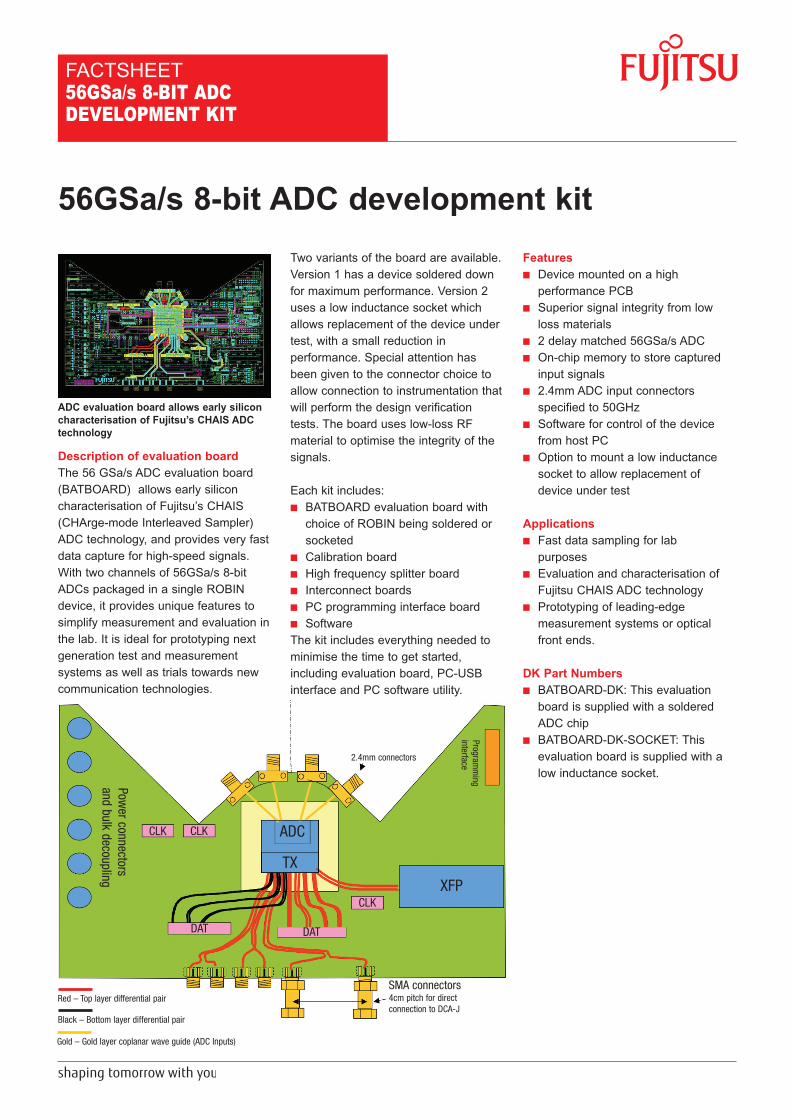
Description of evaluation boardThe 56 GSa/s ADC evaluation board(BATBOARD) allows early siliconcharacterisation of Fujitsu’s CHAIS(CHArge-mode Interleaved Sampler)ADC technology, and provides very fastdata capture for high-speed signals.With two channels of 56GSa/s 8-bitADCs packaged in a single ROBINdevice, it provides unique features tosimplify measurement and evaluation inthe lab. It is ideal for prototyping nextgeneration test and measurementsystems as well as trials towards newcommunication technologies.
Two variants of the board are available.Version 1 has a device soldered downfor maximum performance. Version 2uses a low inductance socket whichallows replacement of the device undertest, with a small reduction inperformance. Special attention hasbeen given to the connector choice toallow connection to instrumentation thatwill perform the design verificationtests. The board uses low-loss RFmaterial to optimise the integrity of thesignals.
Each kit includes:� BATBOARD evaluation board withchoice of ROBIN being soldered orsocketed
� Calibration board� High frequency splitter board� Interconnect boards� PC programming interface board� SoftwareThe kit includes everything needed tominimise the time to get started,including evaluation board, PC-USBinterface and PC software utility.
Features� Device mounted on a highperformance PCB
� Superior signal integrity from lowloss materials
� 2 delay matched 56GSa/s ADC� On-chip memory to store capturedinput signals
� 2.4mm ADC input connectorsspecified to 50GHz
� Software for control of the devicefrom host PC
� Option to mount a low inductancesocket to allow replacement ofdevice under test
Applications� Fast data sampling for labpurposes
� Evaluation and characterisation ofFujitsu CHAIS ADC technology
� Prototyping of leading-edgemeasurement systems or opticalfront ends.
DK Part Numbers� BATBOARD-DK: This evaluationboard is supplied with a solderedADC chip
� BATBOARD-DK-SOCKET: Thisevaluation board is supplied with alow inductance socket.
ADC evaluation board allows early siliconcharacterisation of Fujitsu’s CHAIS ADCtechnology
Black – Bottom layer differential pair
Red – Top layer differential pair
Gold – Gold layer coplanar wave guide (ADC Inputs)
4cm pitch for directconnection to DCA-J
SMA connectors
2.4mm connectors
CLK CLK ADC
TX
XFPCLK
DAT DAT
Programm
inginterface
Powerconnectors
andbulk
decoupling
BATBOARD factsheet:BATBOARD factsheet 16/9/10 16:01 Page 1
2
FACTSHEET56GSa/s 8-BIT ADCDEVELOPMENT KIT
FSEU-C49-06SEP10
Description of CMOS ADC
Fujitsu’s ultra-fast CMOS ADC enables
upcoming telecommunication
applications, such as 100G Ethernet
and OTU-4 transport systems using
coherent receivers. The ADC uses
Fujitsu’s revolutionary CHarge-mode
Interleaved Sampler technology
(CHAIS), which allows the
implementation of extremely fast and
high resolution ADCs in CMOS process
technology.
Major benefits of the CHAIS ADC are
low power consumption and the
possibility to be integrated with millions
of gates onto the same die using
Fujitsu’s standard 65nm CMOS process
technology. In combination with
Fujitsu’s leading flip-chip packaging
technology, the ultra-fast ADC is ideal
for applications that require high
performance analogue and huge digital
processing power while maintaining a
reliable and proven manufacturing flow.
ASK FUJITSU SEMICONDUCTOR EUROPE
Contact us on +49(0) 61 03 69 00 or visithttp://emea.fujitsu.com/networking
ADC Target Applications
� Test equipment
� Fast data conversion
� Optical communications systems
Features
� Fujitsu 65nm CMOS process
technology
� Resolution: 8-bit
� Sampling rate: 56GSa/s
� Power supply: -1.2V, 1.2V, 3.3V
� Power consumption: 2W per
channel (typical)
� DNL: ±0.5 LSB, INL : ±1.0 LSB
� SNDR: 40dBFS @Fin=1GHz,
36dBFS @Fin=17GHz
� Differential analogue Input:
1.0VPPD� >15GHz -3dB input bandwidth
� Two’s complement data format
� Output rate: 128 samples x
8-bit @437.5MHz
� 1.75GHz input reference clock
� Internal 14GHz VCO/PLL per I/Q
ADC pair
� 56GSa/s ADCs configured as two
I/Q Pairs
� <100fs rms jitter
� <500fs I/Q sample time error
� Continuous background calibration
for sampler interleave timing skew
as well as linearity and offset
� Calibration warning and over-range
flags
� Designed for flip-chip
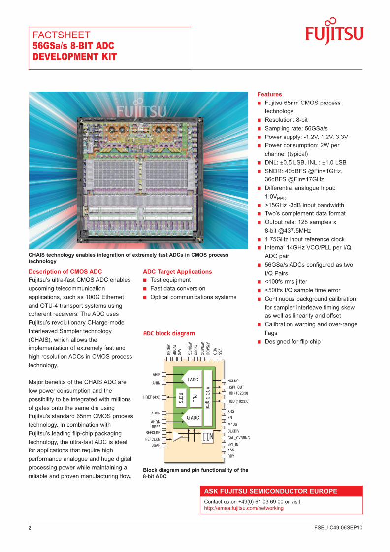
CHAIS technology enables integration of extremely fast ADCs in CMOS processtechnology
AHIP
AHIN
HREF (4:0)
AHQP
AHQNRREF
REFCLKP
REFCLKN
BGAPXSS
RDY
SPI_IN
CAL_OVRRNG
M40G
CLKDIV
EN
XRST
HSPI_OUTHID (1023:0)
HQD (1023:0)
VSSVD
D
AVSADC
AVDAD
C
AVD33
AVDN
EG
AVSAVD
RFAVD
BB
I ADC
Q ADC
∏N
PLL
ADC
Digital
REFS
HCLKO
Block diagram and pin functionality of the8-bit ADC
ADC block diagram
BATBOARD factsheet:BATBOARD factsheet 16/9/10 16:01 Page 2


