
Leti Devices Workshop | December 3, 2017
3D INTEGRATION, A SMART WAY TO ENHANCE PERFORMANCE
| 2
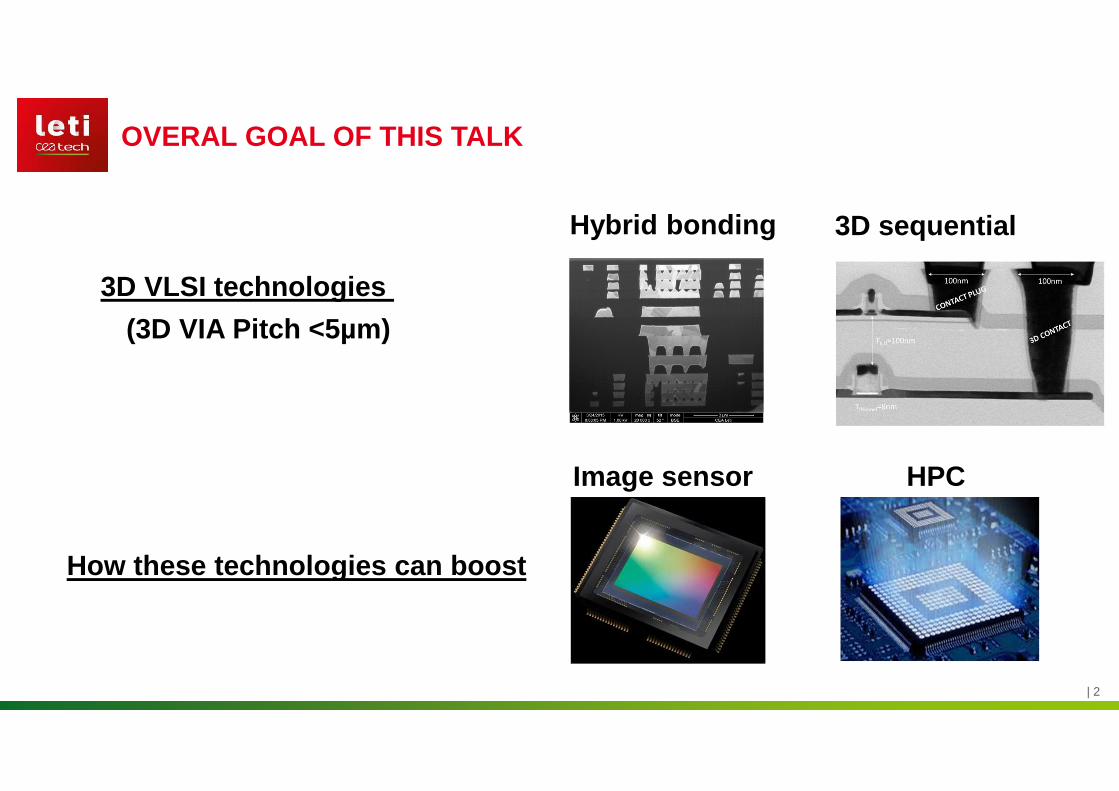
OVERAL GOAL OF THIS TALK
3D VLSI technologies
Hybrid bonding 3D sequential
How these technologies can boost
Image sensor HPC
(3D VIA Pitch <5µm)

| 3
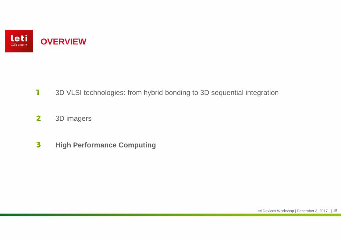
3D VLSI technologies: from hybrid bonding to 3D sequential integration
High Performance computing
3D imagers
OVERVIEW
Leti Devices Workshop | December 3, 2017

| 4Leti Devices Workshop | December 3, 2017
3D VLSI: HYBRID BONDING AND 3D SEQUENTIAL OPTIONS
Hybrid bonding flow:
Base wafer with Cu pad Polishing preparation Wafer bonding Thermal annealing
Various options: Wafer to Wafer, Die to Wafer, Die t o Die
| 5Leti Devices Workshop | December 3, 2017
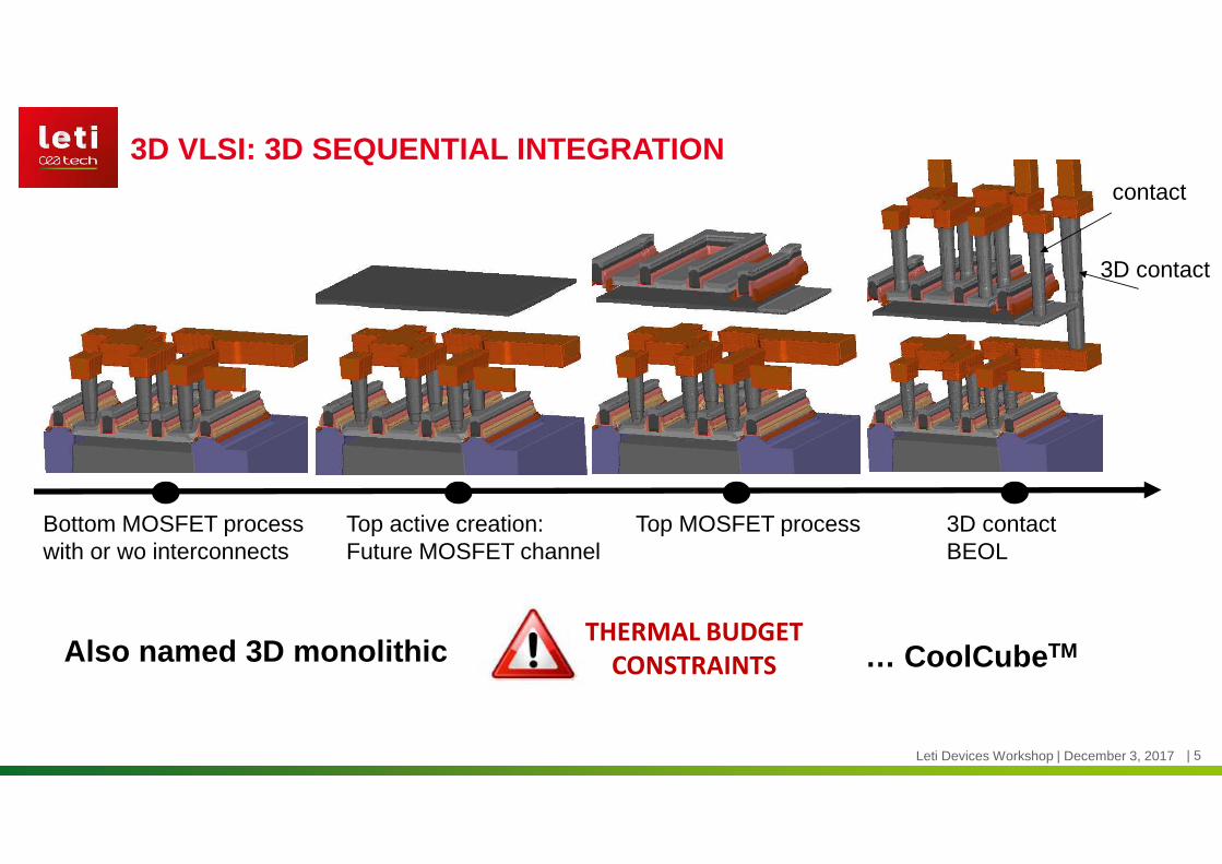
3D VLSI: 3D SEQUENTIAL INTEGRATION
THERMAL BUDGET
CONSTRAINTS
Bottom MOSFET processwith or wo interconnects
Top active creation:Future MOSFET channel
Top MOSFET process 3D contactBEOL
Also named 3D monolithic
contact
3D contact
… CoolCube TM

| 6Leti Devices Workshop | December 3, 2017
3D VLSI: HYBRID BONDING VERSUS 3D SEQUENTIAL
Hybrid bonding
3D sequential
Alignment made during bonding3σ min = 250nm
Alignment by lithography3σ = 5nm (28nm stepper)

| 7Leti Devices Workshop | December 3, 2017
0,1 1 10104
105
106
107
108
109
3D v
ia d
ens
ity (#/
mm
2)
3D contact pitch (µm)
[5]
[4]
[2][3]
[1]3DSI
Packaging 3D
2x10⁷ via/mm2
3D VLSI: HYBRID BONDING & 3D SEQUENTIAL OPTIONS: VIA DENSITY
GranularityGranularity scalescale
1-Entire core 2-Logic bloc 3-Logic gates 4-Transistors
Hybrid bonding
3D sequential
[1]: L. Brunet et al., VLSI 2016, [2] I. Sugaya et al., ASMC 2015, [3] J. De Vos, 3DIC 2016 [4] L. Peng et al., EPTC 2016 [5] D. Zhang et al. TSM 2015
3D via density 3D partitioning options

| 8
3D VLSI technologies: from hybrid bonding to 3D sequential integration
High Performance computing
3D imagers
OVERVIEW
Leti Devices Workshop | December 3, 2017

| 9Leti Devices Workshop | December 3, 2017
3D IMAGERS: CURRENT PARTITIONING TRENDS
Leti Devices Workshop | December 3, 2017
Current Imager system
Form & Fill factor gain wrt 2DEnergy efficiency and performance[1]
[1] Retine leti [2] SONY ISSCC 2017 [3] SONY ISSCC 2017, [3] SONY VLSI 2017
Sony [2] Samsung
2-la
yer
imag
er +
DR
AM
Sony [3] Sony [4]
Parallel access to pixel array1 ADC / 10x16 pixels
Conversion and processing at column level1 ADC + 1 PE / column
“Motion EyeTM”
| 10
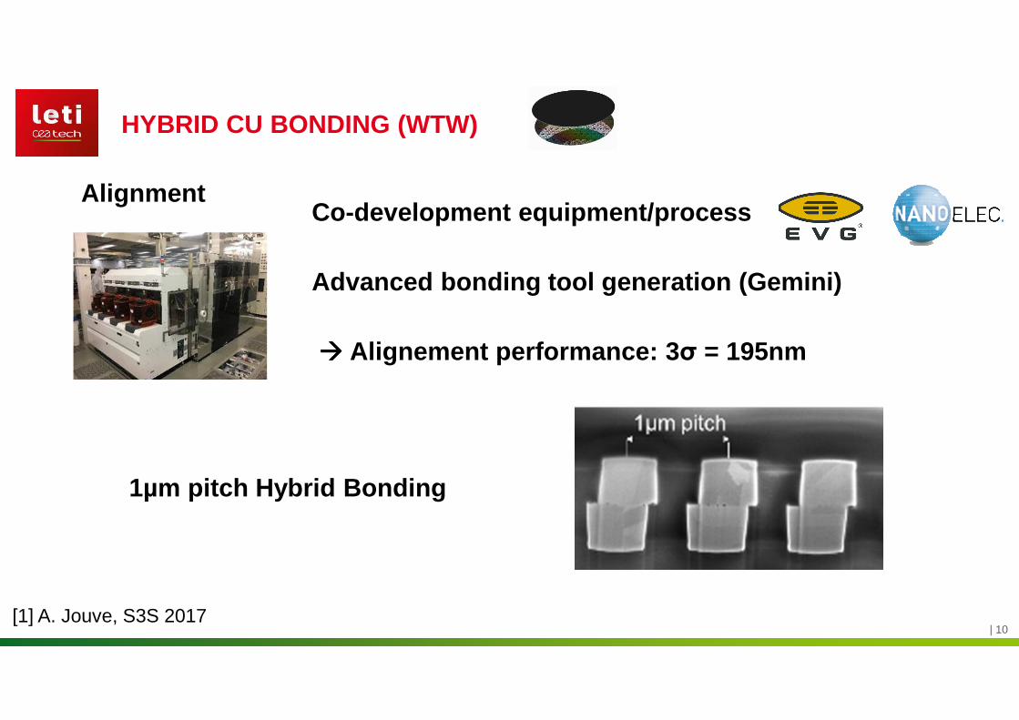
HYBRID CU BONDING (WTW)
Co-development equipment/process
Advanced bonding tool generation (Gemini)
���� Alignement performance: 3 σ = 195nm
Alignment
1µm pitch Hybrid Bonding
[1] A. Jouve, S3S 2017
[1]
| 11Leti Devices Workshop | December 3, 2017
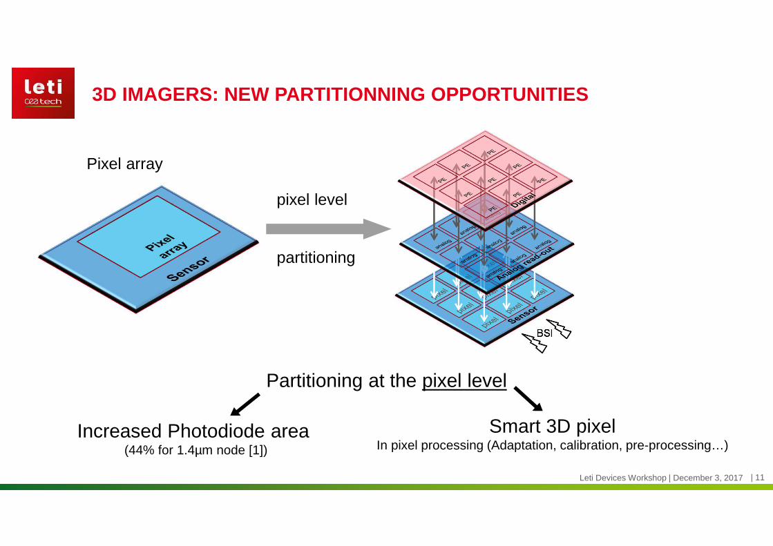
pixel level
partitioning
Pixel array
3D IMAGERS: NEW PARTITIONNING OPPORTUNITIES
Partitioning at the pixel level
Smart 3D pixelIn pixel processing (Adaptation, calibration, pre-processing…)
Increased Photodiode area (44% for 1.4µm node [1])

| 12Leti Devices Workshop | December 3, 2017
pixel level
partitioning
Pixel array
3D IMAGERS: NEW PARTITIONNING OPPORTUNITIES
Hybrid bonding can be used to connect the 3D pixel to the DSP and RAM

| 13
3D IMAGERS: NEW PARTITIONNING OPPORTUNITIES
Leti Devices Workshop | December 3, 2017
<1µm 3D contact pitch 3D sequential integration
300 mm industrial clean room demonstrationMax TB budget is relaxed for a photodiode (700°C) [1] vs MOSFET (500°C)
0 2 4 6 8 10
400
600
Tem
pera
ture
(°C
)
Anneal duration (h)
MOS stability region
[1]P. Coudrain et al., IEDM 2008

| 14Leti Devices Workshop | December 3, 2017
Critical process modules are now below 500°C
Cold 28nm FDSOI devices in line with high-temp. POR
3D IMAGERS: NEW PARTITIONNING OPPORTUNITIES
-800 -600 -400 -200 0 200 400 600 800
-10
-8
-6
-4
VDD
=1VW=1µm
1E
1E
1E
1E
I OFF
(A/µ
m) @
VT_
LIN -
0,2V
Ion ( µµµµA/µµµµm) @ VT_LIN
+ 0,7V
HT POR LT, tilt 7°
HT POR LT, tilt 15° LT, tilt 25°
| 15
3D VLSI technologies: from hybrid bonding to 3D sequential integration
High Performance Computing
3D imagers
OVERVIEW
Leti Devices Workshop | December 3, 2017
| 16
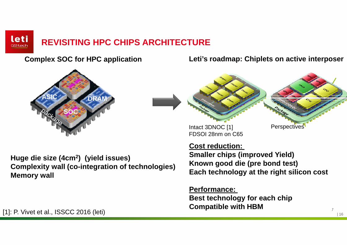
REVISITING HPC CHIPS ARCHITECTURE
Leti Devices Workshop | December 3, 2017
Passive, Active, Photonics
Complex SOC for HPC application Leti’s roadmap: Chiplets on active interposer
Huge die size (4cm 2) (yield issues)Complexity wall (co-integration of technologies)Memory wall
Cost reduction: Smaller chips (improved Yield)Known good die (pre bond test)Each technology at the right silicon cost
Performance: Best technology for each chipCompatible with HBM
Intact 3DNOC [1] FDSOI 28nm on C65
Perspectives
SOC
DRAMASIC
[1]: P. Vivet et al., ISSCC 2016 (leti)

| 17
DIE TO WAFER WITH SCALED CONTACT PITCH
Leti Devices Workshop | December 3, 2017[1] P. Metzger & Al « Toward a flip-chip bonder dedicated to direct bonding for productionenvironment », IWLPC 2017.
1.CMP 2. Top die dicing 3. Holder placement
Die-to-Wafer bonding flow
Top
die
Bot
tom
waf
er
1.CMP 2.Plasma activation (optionnal)
4. Cleaning
5. Die-to-Wafer stacking
FC1 Results� Precision: ± 1 µm� Throughput: 500 dph
3µm pitch DTWhybrid bondingdemonstrated
Gen 2: FC1 tool [1]
| 18
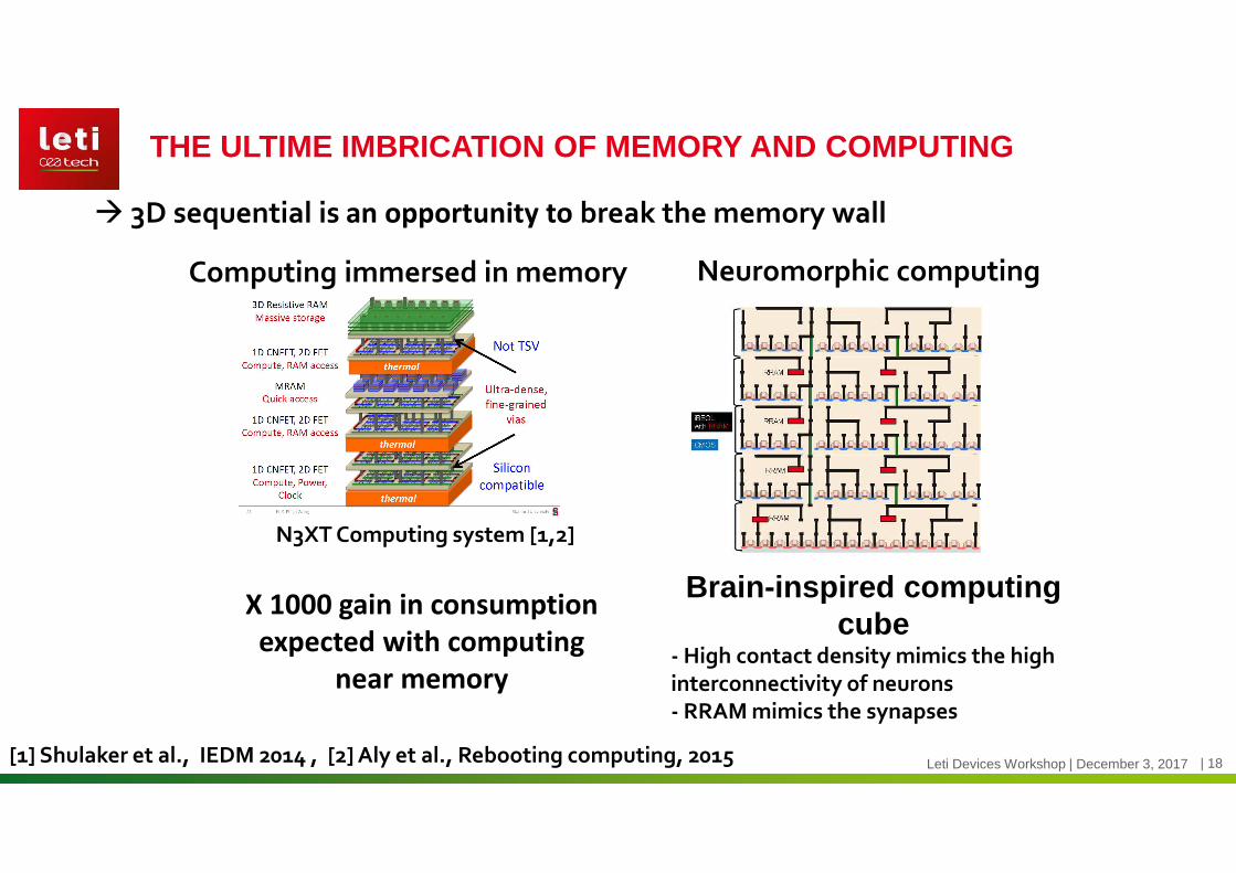
THE ULTIME IMBRICATION OF MEMORY AND COMPUTING
Leti Devices Workshop | December 3, 2017
Computing immersed in memory
N3XT Computing system [1,2]
X 1000 gain in consumption
expected with computing
near memory
[1] Shulaker et al., IEDM 2014 , [2] Aly et al., Rebooting computing, 2015
� 3D sequential is an opportunity to break the memory wall
Neuromorphic computing
Brain-inspired computingcube
- High contact density mimics the high interconnectivity of neurons- RRAM mimics the synapses
| 19
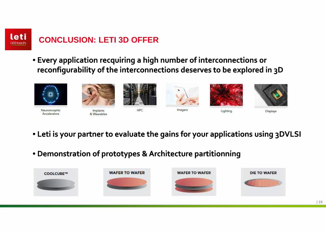
CONCLUSION: LETI 3D OFFER
• Leti is your partner to evaluate the gains for your applications using 3DVLSI
• Demonstration of prototypes & Architecture partitionning
• Leti is your partner to evaluate the gains for your applications using 3DVLSI
• Demonstration of prototypes & Architecture partitionning
• Every application recquiring a high number of interconnections or
reconfigurability of the interconnections deserves to be explored in 3D
• Every application recquiring a high number of interconnections or
reconfigurability of the interconnections deserves to be explored in 3D

| 20
3D INTEGRATION, A SMART WAY TO ENHANCE PERFORMANCE
Leti Devices Workshop | December 3, 2017
Thank you for your attention


