Download - 2 Op Amp Concepts

Operational Amplifiers:Basic Concepts
Prof. Greg Kovacs
Department of Electrical Engineering
Stanford University

EE122, Stanford University, Prof. Greg Kovacs 2
Design Note: The Design Process
• Definition of function - what you want.
• Block diagram - translate into circuit functions.
• First Design Review.
• Circuit design - the details of how functions areaccomplished.
– Component selection– Schematic– Simulation– Prototyping of critical sections
• Second Design Review.
• Fabrication and Testing.

EE122, Stanford University, Prof. Greg Kovacs 3
EE122 Parts Kit

EE122, Stanford University, Prof. Greg Kovacs 4
Parts Kit Guide
Sockets
LT1056 Op-Amps
LM334 Temp. Sensor
SFH300-3BPhototransistor
CdS Cell
Bright Red LEDs
Yellow LEDs
LT1167Instrum.
Amp
LT1175AdjustableNegativeVoltage
RegulatorAD654 V-FConverter
LT1011Comparator
555 Timer
LTC1064-2SwitchedCapacitor
Filter
7805 +5VRegulator
MJE3055 NPNPower Transistor
IRLZ34 Logic-Level PowerMOSFET (N-Chan)
LT1036 VoltageRegulator +12/+5
LT1033 VoltageRegulator 3A Negative,Adjustable

EE122, Stanford University, Prof. Greg Kovacs 5
Protoboards...
Each set of five pins are shortedtogether internally so you canmake multiple connections to onei.c. pin or component lead...
Each of the long rows of pins is shortedtogether so you can use them as powersupply and ground lines...

EE122, Stanford University, Prof. Greg Kovacs 6
USE decoupling capacitors (typically0.1 µF) from each power supply rail toground. This is essential to preventunwanted oscillations.
The capacitors locally source and sinkcurrents from the supply rails of the chips, preventing them from “talking” to each other and their own inputs!

EE122, Stanford University, Prof. Greg Kovacs 7
Point-To-Point SolderingOn A Ground-Planed Board

EE122, Stanford University, Prof. Greg Kovacs 8
What Is an Op-Amp Anyway?OBJECTIVES (Why am I sitting in this classroom?)
• To obtain a practical understanding of what operationalamplifiers (“op-amps”) are and some applications theycan be used for.
• To understand the basic op-amp circuit configurations.
• To understand the basic characteristics (good and bad)of op-amps before measuring some of them in the lab.
• To keep your parents happy!
"We don't need no education...."We don't need no education....

EE122, Stanford University, Prof. Greg Kovacs 9
The Ideal Op-Amp
+-
V2
V1
A(V2-V1)
1) The input impedance isinfinite - i.e. no current everflows into either input of theop-amp.
2) The output impedance iszero - i.e. the op-amp candrive any load impedance toany voltage.
3) The open-loop gain (A) isinfinte.
4) The bandwidth is infinite.
5) The output voltage is zerowhen the input voltagedifference is zero.
The Op-Amp produces an outputvoltage that is the difference betweenthe two input terminals, multiplied bythe gain A...

EE122, Stanford University, Prof. Greg Kovacs 10
Types of Op-Amps
Traditional costumes of analog circuit designers.
NICE HAT!
• Low power
• Low noise
• Low offset
• High power
• High voltage
• High speed
• Single
• Dual
• Quad

EE122, Stanford University, Prof. Greg Kovacs 11
A Bit of History...
• The first Op-Amps were invented during the timeof the Second World War...
• Dr. C. A. Lovell of Bell Telephone Laboratoriesintroduced the Op-Amp...
• George A. Philbrick independently introduced asingle vacuum tube operational amplifier in 1948.
• SO, Op-Amps are NOT new!
• The ever-popular 741 monolithic Op-Amp wasdesigned by Dave Fullagar in 1967....

EE122, Stanford University, Prof. Greg Kovacs 12
The First "Real" OpAmp -> The K2-W
12AX7 12AX7
220K
1M
220K 2.2M
510K
221K
9.1K
500pF
120K
4.7M
7.5pF
680K
NE-68
NE-68
+300 VDC
-300 VDC
- Vin
+ VinVout

EE122, Stanford University, Prof. Greg Kovacs 13
K2-XA

EE122, Stanford University, Prof. Greg Kovacs 14
The K2-W Tube OpAmp• Invented by Julie Loebe and George Philbrick (early 1950's)• The first "mass production" OpAmp...• Cost (in 1950's) approximately $22.00...• Basic specifications comparison to 741 and LT1037...
Parameters K2-W OpAmp 741 OpAmp LT1037OpAmp
Power Supplies +/- 300 VDC,6.3 VAC(filaments)
+/- 15V +/- 15V
Open-LoopGain
1.5X10⁴ 5X10⁴ 30X106
Vout Swing +/- 50V +/- 12V +/- 13.5 VIout +/- 1 mA 25 mA 25 mAIdrain 5 mA (no load) 1.7 mA 2.7 mARL(min) 50 KΩ none (SC
protect)none (SCprotect)
Slew Rate +/- 12 V/µSec +/- 0.5 V/µS 15 V/µS

EE122, Stanford University, Prof. Greg Kovacs 15
Good Op-Amp Web Sites
• www.linear-tech.com
• www.national.com
• www.burr-brown.com
• www.maxim-ic.com
• www.intersil.com

EE122, Stanford University, Prof. Greg Kovacs 16
Cool New Project/DesignWebsite:
www.designnotes.com
Submit your favorite circuit or program. Everymonth the best design entry (judged by yourpeers), wins $100 in cash! Monthly winners areeligible for the $1200 Grand Prize!

EE122, Stanford University, Prof. Greg Kovacs 17
Courtesy Mr. Charlie Kiers.

EE122, Stanford University, Prof. Greg Kovacs 18
Op-Amp Datasheets for EE122:Some Example Devices
• LM741 (basic)
• LT1056 (JFET input)
• LMC660 (CMOS - low power)
• LT1220/1221 (fast)
• LM675 (medium power)
• LM12 (high power)

EE122, Stanford University, Prof. Greg Kovacs 19
The Ideal Op-Amp In SPICE
EXXXXXXX N+ N- NC+ NC- GAIN
Eout 3 0 1 2 100K
Use a voltage-controlled voltage source:
+-
V2
V1
A(V2-V1)
0
1
2
3
EE122, Stanford University, Prof. Greg Kovacs 20
2
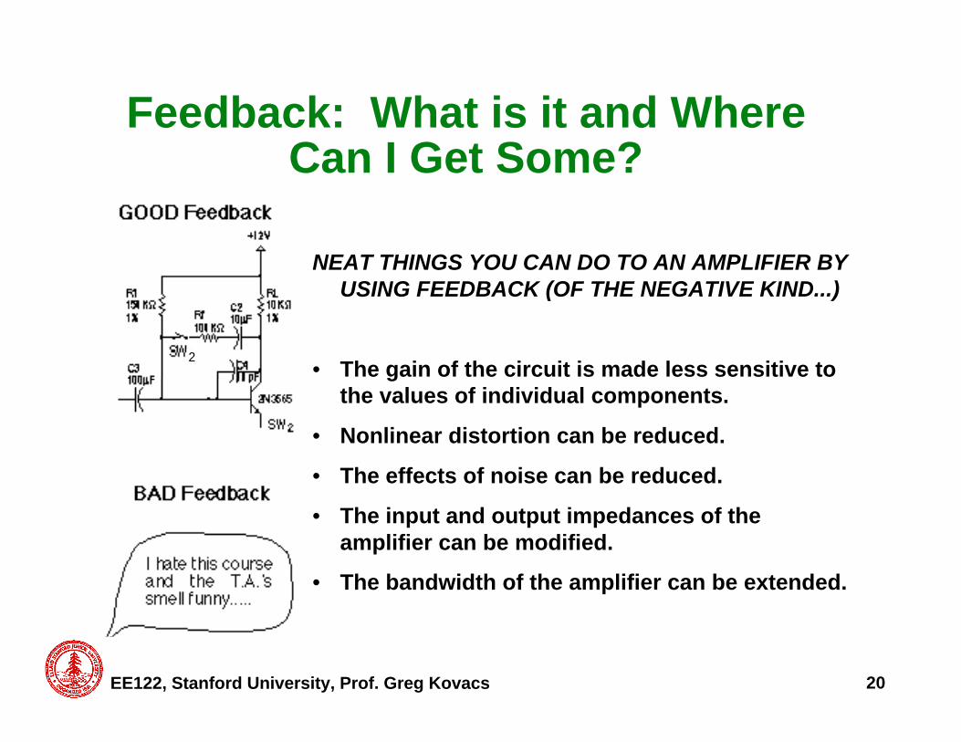
Feedback: What is it and WhereCan I Get Some?
NEAT THINGS YOU CAN DO TO AN AMPLIFIER BYUSING FEEDBACK (OF THE NEGATIVE KIND...)
• The gain of the circuit is made less sensitive tothe values of individual components.
• Nonlinear distortion can be reduced.
• The effects of noise can be reduced.
• The input and output impedances of theamplifier can be modified.
• The bandwidth of the amplifier can be extended.

EE122, Stanford University, Prof. Greg Kovacs 21
WHAT CAN YOU DO WITH OP-AMPS?
• Feed the hungry.
• Amplify signals.
• Heal the sick.
• Buffer signals.
• End global warming.
• Integrate signals.
• Save the dolphins.
• Differentiate signals.
• Pay off the deficit.
• Sum multiple signals.
• Make music very loud!

EE122, Stanford University, Prof. Greg Kovacs 22
Jim Williams

EE122, Stanford University, Prof. Greg Kovacs 23
AnalogHacker’s Bible

EE122, Stanford University, Prof. Greg Kovacs 24
THE VOLTAGE FOLLOWER
V- VOUTV+
VIN
V- = VOUT
VOUT = AV+ - V-
VOUT = A1 + A
V+
1
What is it good for?
Buffering a high-impedance signal to "beat"Heisenberg... You don't load it down when youmeasure it...
It has the best bandwidth of any op-amp circuit.
Some op-amps need to be COMPENSATED forstable unity-gain operation (more later....).

EE122, Stanford University, Prof. Greg Kovacs 25
THE INVERTING AMPLIFIER
R2
R1
iin
i fb
VOUTVIN V-
V+
The V- terminal is referred to as a "virtual ground"... Why is that?
THIS IS A KEY POINT!!!
Due to NEGATIVEFEEDBACK!!!!
AV = −R2
R1
VOUT = A 0 − V−( )thus,
V− = VOUT
A≈ VOUT
∞= 0

EE122, Stanford University, Prof. Greg Kovacs 26
Op-Amp Application: CLIPPER(or "Fuzz Box")
R2
R1
Mellow Tunes
INHeavy Metal
OUT
Input signal must be large
enough to turn on diodes...

EE122, Stanford University, Prof. Greg Kovacs 27
THE NON-INVERTING AMPLIFIER
R1
R2
i1
i2
VOUT
VIN
V-
V+
A key point to note here is that the V- node is not a virtualground in this configuration!
The important thing to consider is that the voltagedifference between V+ and V- is kept near zero. In otherwords, V- VIN.
AV = 1+R2
R1

EE122, Stanford University, Prof. Greg Kovacs 28
THE SUMMING AMPLIFIERRf
R3
R2
R1
R4
Rn
i f
VOUT
V1
V
V-
+
V2
V3
V4
Vn
i1
What is it good for?
Summing multiple input signals in anyproportion desired (determined by the relativevalues of the input resistors.
Averaging signals (do you know how?).
VOUT = −V1
Rf
R1− V2
Rf
R2−L − VN
Rf
RNor,
VOUT = −RfVi
Ri
i∑

EE122, Stanford University, Prof. Greg Kovacs 29
NoiseCanceling
Circuit

EE122, Stanford University, Prof. Greg Kovacs 30
Instrumentation Amplifier
Source: Sedra, A. S., andSmith, K. C., “MicroelectronicCircuits,” Oxford, 1998.
AV = −R4
R3
1+2R2
R1
For one-resistor gain adjust, set R4 = R3 and fix R2.
• Very high input impedance.
• Gain can be set with only one resistor.
• Can optimize CMRR.

EE122, Stanford University, Prof. Greg Kovacs 31
Op-Amp Application: EKG
Instrumentation Amplifier
Filter (0.04 - 150 Hz)
Source: Webster, J. G.,“Medical Instrumentation:Application and Design,”Houghton Mifflin, 1978.

EE122, Stanford University, Prof. Greg Kovacs 32
A Safe Heart Signal Interface
Polar™ heart-rate transmitter - provides magnetically coupled bursts of 5 kHz energy thatmark the start of each heartbeat (i.e., you don’t get the actual waveform).
www.polarusa.com

EE122, Stanford University, Prof. Greg Kovacs 33
Polar™ OEM Receiver

EE122, Stanford University, Prof. Greg Kovacs 34
THE INTEGRATOR
R2
R1
C1
VOUT
V
V-
+
VIN
iin
VOUTVIN
= - R2R1
For DC inputs:
Need R2 to make the integrator "leaky"... Otherwise small DC offsets wouldcharge it up (and up, and up!!!!).
iin = ifbvinR1
= - C1d voutdt
vout = - 1R1 C1
vindt
For AC inputs:What is it good for?
Triangle wave generation.
Ramp generation ('scopes!).
Math (yuk) as it used to be done!
What kind of filter is this?

EE122, Stanford University, Prof. Greg Kovacs 35
OP-AMP INTEGRATOR SIMULATIONOp-Amp Integrator Simulation*YOU fill in the component values!R1 1 2 ?CI2 2 3 ?R2 2 3 ?E1 3 0 0 2 100KVin 1 0 pulse(-1 1 0 5nS 5nS 500uS 1mS).TRAN 100uS 10mS.probe.end
R2
R1
C1
VOUT
V
V-
+
VIN
iin
1 23
0
0.0S 2mS 4mS 6mS 8mS 10mS
mS
-10V
0.0V
10V
V
TIMEtran3
V(1) V(3)

EE122, Stanford University, Prof. Greg Kovacs 36
Insect LarvaContaining
Candy

EE122, Stanford University, Prof. Greg Kovacs 37
THE DIFFERENTIATORR2
R1 C1
VOUT
V
V-
+
VIN
iin
if
vout = - R2 C1 dvindt
What kind of filter is this?
R1 is needed to limit the high-frequencygain (noise may be small, but it can havea very large derivative!).
Design the circuit to be usedbelow this frequency
fmax = 12π R1 C1

EE122, Stanford University, Prof. Greg Kovacs 38
INTEGRATOR/DIFFERENTIATORSIMULATION
10mS 11mS 12mS
mS
-2V
0.0V
2V
V
TIMEtran2
V(1) V(3) V(6)
Why don't you get out what you put in?

EE122, Stanford University, Prof. Greg Kovacs 39
"REAL" OP-AMPS DO EATQUICHE
1) The input impedance is infinite- i.e. no current ever flows intoeither input of the op-amp.
2) The output impedance is zero -i.e. the op-amp can drive anyload impedance to any voltage.
3) The open-loop gain (A) isinfinte.
4) The bandwidth is infinite.
5) The output voltage is zerowhen the input voltagedifference is zero.
NO, but it is often GIGAor TERA !
NO, but is can be a fewohms in many cases!
NO, but it is usuallyseveral million!
NO, usually several MHz.
NO, offset voltages exist,but can be trimmed.
NO, but it is often GIGAor TERA !
NO, but is can be a fewohms in many cases!
NO, but it is usuallyseveral million!
NO, usually several MHz.
NO, offset voltages exist,but can be trimmed.
What You WANT What You GET

EE122, Stanford University, Prof. Greg Kovacs 40
SLEW RATEOp-Amps can only swing their outputs
so fast...
If you try an make them go faster, theytry, but you get a limiting rate ofchange, the SLEW RATE!
Measuring theSLEW RATE ofa lobster usinga piece ofBungie-cord...
0us 5us 10us 15us 20us
TimeV(1) V(2)
2.0V
0.0V
-2.0V
Exit Add_trace Remove_trace X_axis Y_axis Plot_control Display_control Macros Hard_copy Cursor Zoom Label
Simulated slew-rate-limitedunity-gain amplifier with aUA741 op-amp
3.9 µS to swing 2 Vgives a slew rate of 0.5 V/µS

EE122, Stanford University, Prof. Greg Kovacs 41
Slew Rate Example - Rising
LM741 (slow) and LT1056, ±15V Supplies, 2k Load, 1VPP Squarewave Input (locally terminated into 50 ).

EE122, Stanford University, Prof. Greg Kovacs 42
Slew Rate Example - Falling
LM741 (slow) and LT1056, ±15V Supplies, 2k Load, 1VPP Squarewave Input (locally terminated into 50 ).

EE122, Stanford University, Prof. Greg Kovacs 43
“Ultra Stealth Airplane”

EE122, Stanford University, Prof. Greg Kovacs 44
Gain-Bandwidth Product is Constant
This animation shows the how the bandwidth of an op-amp in the inverting configurationincreases as the gain is decreased.

EE122, Stanford University, Prof. Greg Kovacs 45
OPEN-LOOP CHARACTERISTICSOF "REAL" OP-AMPS
1.0h 3.0h 10h 30h 100h
FrequencyV(5)/ V(1)
1.0M
100K
10K
100Kh 300Kh 1.0Mh 3.0Mh 10Mh
FrequencyV(5)/ V(1)
100
1.0
10m
3 dB frequency fu is VERY LOW!
Unity-gain frequency fT can be
VERY HIGH (many MHz)!
fT
uf
This frequency is determinedby the "Dominant Pole" of theop-amp.
If negative feedback is applied,fu may be shifted to muchhigher frequencies
For unity-gain connected op-amps, fu is the same as fT.
For any other gain, fT can bedetermined by using the GAIN-BANDWIDTH PRODUCT
fU =fT
Closed − Loop _Gain

EE122, Stanford University, Prof. Greg Kovacs 46
STABILITY AND COMPENSATIONWith negative feedback, if the input of
the amplifier receives a -180° out-of-phase replica of the output signal(via the feedback circuit) you end upwith OSCILLATIONS!!!!
All op-amps have a high-frequencyroll-off determined by several poles.This means that eventually, you willhit -180° phase! The key toSTABILITY is to ensure that thishappens when the gain has fallen offto less than 1!
This can be accomplished byDELIBERATELY rolling off theamplifier using a COMPENSATIONCAPACITOR!
This effect isworse at lowergains becauseMORE SIGNAL ISFED BACK!

EE122, Stanford University, Prof. Greg Kovacs 47
MODELING "REAL" OP-AMPS
* UA741 operational amplifier "macromodel" subcircuit* connections: non-inverting input* | inverting input* | | positive power supply* | | | negative power supply* | | | | output* | | | | |.subckt UA741 1 2 3 4 5*c1 11 12 4.664E-12c2 6 7 20.00E-12dc 5 53 dxde 54 5 dxdlp 90 91 dxdln 92 90 dxdp 4 3 dxegnd1 98 0 3 0 0.500000egnd2 99 98 4 0 0.500000fb1 7 99 vb 10610000.000000fb2 7 99 vc -10000000.000000fb3 7 99 ve 10000000.000000fb4 7 99 vlp 10000000.000000fb5 7 99 vln -10000000.000000ga 6 0 11 12 137.7E-6
gcm 0 6 10 99 2.574E-9iee 10 4 dc 10.16E-6hlim 90 0 vlim 1Kq1 11 2 13 qxq2 12 1 14 qxr2 6 9 100.0E3rc1 3 11 7.957E3rc2 3 12 7.957E3re1 13 10 2.740E3re2 14 10 2.740E3ree 10 99 19.69E6ro1 8 5 150ro2 7 99 150rp 3 4 18.11E3vb 9 0 dc 0vc 3 53 dc 2.600ve 54 4 dc 2.600vlim 7 8 dc 0vlp 91 0 dc 25vln 0 92 dc 25.model dx D(Is=800.0E-18).model qx NPN(Is=800.0E-18 Bf=62.50).ends
The WORSE the op-amp, the more work it takes to model it!
IDEAL OP-AMP:Eout 3 0 1 2 100K
CRAPPY, OBSOLETE OP-AMP:

EE122, Stanford University, Prof. Greg Kovacs 48
EXAMPLE OF USING A "REAL"OP-AMP MACROMODEL
X1 1 2 3 4 2 UA741Vplus 3 0 15VVminus 0 4 15VVin 1 0 AC 1 0.AC DEC 100 1hz 10MEG.probe.end
NOTE:1) You declare an "instance"of your macromodel with aname that begins with "X"
2) You have to explicitlydefine the power supplies.
1.0h 100h 10Kh 1.0Mh 10Mh
FrequencyV(5)/V(1)
1.0M
100
10m

EE122, Stanford University, Prof. Greg Kovacs 49
SPAM ZAPPED WITH PHOTONS!

EE122, Stanford University, Prof. Greg Kovacs 50
CONCLUSION
• Op-Amps are useful for lots of things.
• Op-Amps deliver a lot of performance for peanuts!
• Op-Amp circuits are generally fairly intuitive if youremember the basic "rules" of op-amp operation!


