download the st35-efb installation manual - tronola
TRANSCRIPT

D. Gillespie DesignsST-35 Capacitor Board
Installation Manual
with EFBTM
D. Gillespie Designs www.tronola.com

Part of the EFB™ modification involves wiring changes, and adding resistors to, the output tube sockets. Care must be taken when unsoldering the wires going to the output transformers. Sometimes the original builder will have left little or no extra length to allow you to just cut the wires off. To avoid unsightly and messy splicing these wires must be carefully unsoldered to preserve the length.
Useful Tools:
De-solder braid and a vacuum de-soldering pump are indispensable items when attempting to remove solder from existing connections, such as the tube sockets. They are inexpensive and available from suppliers such as DigiKey and Mouser Electronics
Thank you for choosing our ST-35 Capacitor Board with *EFB™. We feel it is the single most significant upgrade you can make to your Dynaco ST-35 and is designed to integrate into the amplifier without chassis modifications of any kind.
The ST-35 Capacitor EFB™ Board replaces the original multi section power supply filter capacitor as well as all the associated resistors and high voltage rectifier diodes. Besides larger overall capacitance, additional metalized polypropylene bypass capacitors have also been included. The original cathode bias resistor has been replaced with an innovative Enhanced Fixed Bias feature that allows your ST-35 to perform to its full potential with both channels driven. Although rated at 17.5W per channel output power, this is really only true if only a single channel is driven. With both channels driven, however, power output is typically closer to 14W per channel, and distortion is significantly higher as well. This is largely due to various compromises related to the use of the simple, but economical, cathode bias system. *
Please follow this manual carefully to ensure a successful and safe installation.
During installation you may want to refer to the original assembly manual. If you do not have one, a free copy may be downloaded at: www.tubes4hifi.com
NOTE: Installation of the EFB™ board requires intermediate to advanced soldering skills. Very tight spacing for the connection eyelets on the board requires that you posses very good soldering skills as well as a suitable soldering iron. If you are a novice it is recommended that you seek out the services of someone qualified to perform the installation.
NOTE:
The modified ST-35 still requires a matched quad of output tubes. This was done on purpose to minimize the extent of changes required, to maintain as much of the original design concept as possible, and because it generates nearly all of the improvement possible. Also, this is always a worthwhile investment in achieving matched performance from both channels.
EFB™
EFB™ is a new and innovative way to convert your ST-35 to fixed bias operation and reveal its full potential. Rated power output will be maintained with both channels driven, and distortion significantly reduced. The *EFB™ feature, when combined with increased power supply capacity, provides an outstanding upgrade to your ST-35.
*EFB™
*EFB™ is a trademark of D. Gillespie Designs.
2

Remove the original power supply components:
Installation Procedure
Before beginning the installation process switch off your ST-35 and disconnect the power cord from the AC outlet. Wait at least 30 minutes before removing the top and bottom covers. This will allow time for the voltage on the power supply capacitors to bleed off. !
Refer to Fig. 1 for the following steps:
Locate the 5-lug terminal strip on the bottom side of the chassis. Remove the diodes from terminals 1 and 2 but leave the two transformer wires connected.
Disconnect all the component leads from terminal lug 1of the power supply capacitor..
1
2
3
Fig. 1
HIGH VOLTAGE WARNING
Vacuum tube amplifiers contain lethal voltages. Extreme care must be exercised at all times when working with the top or bottom covers removed when power is applied. If you are not certain of your ability to safely perform the following installation steps it is advised that you seek the services of a qualified technician.
1 Disconnect diodes21
Disconnect all component leads22
Remove the original power supply components ctd:
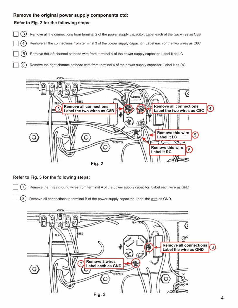
Refer to Fig. 2 for the following steps:
Refer to Fig. 3 for the following steps:
Remove all the connections from terminal 2 of the power supply capacitor. Label each of the two wires as C8B 3
Remove all the connections from terminal 3 of the power supply capacitor. Label each of the two wires as C8C4
Remove the left channel cathode wire from terminal 4 of the power supply capacitor. Label it as LC5
Remove the right channel cathode wire from terminal 4 of the power supply capacitor. Label it as RC6
Remove the three ground wires from terminal A of the power supply capacitor. Label each wire as GND.7
Remove all connections to terminal B of the power supply capacitor. Label the wire as GND.8
Remove all connectionsLabel the two wires as C8B
23 124Remove all connectionsLabel the two wires as C8C
125Remove this wireLabel it LC
126Remove this wireLabel it RC
Fig. 2
Fig. 3
Remove 3 wires Label each as GND
27
28Remove all connectionsLabel the wire as GND
4

Installing the Capacitor EFB™Board:
Wiring the Capacitor EFB™Board:
9 The Capacitor EFB™ board is mounted on five standoff’s which are secured to the chassis from the bottom side, through existing slots. Using the supplied screws and lock washers install the board as shown in Fig. 4 below. Align the front of the board so that it is parallel with the front edge of the chassis, then tighten all bottom side screws securely. If the power transformer interferes with the installation of the EFB™ board, loosen the transformer mounting screws, slide the transformer towards the back of the chassis, and re-tighten the screws. The transformer bell should not be touching the board or any of its components.
5
10 Solder a 3 1/2” length of #20-22 gauge red wire to terminal strip lug 1. Solder another 3 1/2” length of #20-22 gauge red wire to terminal strip lug 2 as shown in Fig. 5. Label the wires as TS-1 and TS-2. Twist the wires together.
Fig. 5
Solder # 20-22 gauge red wires toTS lugs 1 and 2. Label these TS-1 and TS-2
1210
Fig. 4
Slide the power transformer towards the back ofthe chassis if it interferes with EFB installation.

Preparing the PC-13 boards
Remove the wire connecting lug 2 of socket V-2 to eyelet 8 on the left channel PC-13. 11
Refer to Fig. 6 for the following steps.
6
12 Remove the wire connecting lug 2 of socket V-3 to eyelet 9 on the left channel PC-13.
13 Remove the wire connecting lug 2 of socket V-5 to eyelet 8 on the right channel PC-13.
14 Remove the wire connecting lug 2 of socket V-6 to eyelet 9 on the right channel PC-13.
Fig. 6
211 Remove this wire 213 Remove this wire
212Remove this wire
214Remove this wire
Left Ch. Right Ch.
With the conversion to , control grid swamper resistors and screen stability resistors will now be required. These are added at the output tube sockets on the PC-13 boards. The following steps take you through the process of installing these resistors. Note that the supplied metal film resistors are very similar in appearance, and are packaged and labeled separately. Be sure not to mix these up during installation.
EFB™

Preparing the PC-13 boards ctd.
Remove the wire connected to lug 9 of socket V-2 and connect it to lug 8. Do not solder it yet. 15
16 Remove the two wires connected to lug 9 of socket V-3 and connect them to lug 8. Do not solder them yet.
17 Remove the wire connected to lug 9 of socket V-5 and connect it to lug 8. Do not solder it yet.
18 Remove the two wires connected to lug 9 of socket V-6 and connect them to lug 8. Do not solder them yet.
Refer to Fig. 7 for the following steps.
Fig. 7
Depending upon the excess length left by the original kit builder, it may be necessary to add length to some transformer wires. If required, be sure to properly insulate the connection where the join is made (heat shrink tubing, etc.).
Note:
7
Left Ch. Right Ch.
Move these wiresto lug 8
218
Move these wiresto lug 8
216
2Move this wireto lug 8
17
Move this wireto lug 815

Preparing the PC-13 boards
19
22
Connect a 100 ohm 0.5W resistor between lugs 8 and 9 of socket V-2. Solder both lugs.
Connect a 100 ohm 0.5W resistor between lugs 8 and 9 of socket V-3. Solder both lugs.
20
21
Connect a 1K 0.5W resistor between lug 2 of socket V-2 and eyelet 8 on the PC-13. Solder both connections.
Connect a 1K 0.5W resistor between lug 2 of socket V-3 and eyelet 9 on the PC-13. Solder both connections.
Refer to Fig. 8 for the following steps.
Refer to Fig. 9 for the following steps.
23
26
Connect a 100 ohm 0.5W resistor between lugs 8 and 9 of socket V-5. Solder both lugs.
Connect a 100 ohm 0.5W resistor between lugs 8 and 9 of socket V-6. Solder both lugs.
24
25
Connect a 1K 0.5W resistor between lug 2 of socket V-5 and eyelet 8 on the PC-13. Solder both connections.
Connect a 1K 0.5W resistor between lug 2 of socket V-6 and eyelet 9 on the PC-13. Solder both connections.
Fig. 8 Fig. 9
100
1K
100
1K
100
100
1K
1K
8
219
220
221
222
23
24
25
226

Refer to Figs. 10, 11 and 12 for the following steps:
! It is extremely important to complete the following steps exactly in the order indicated.
The following solder connections are made to the eyelets on the bottom side of the Capacitor EFB™ board. The eyelet spacing is very close requiring good soldering skills and a proper soldering iron with an appropriately small tip. Great care will be required to ensure a good solder connection while not melting adjacent wires, or creating solder bridges, as the process continues step by step.
In preparation for inserting and soldering to the board eyelets, each wire should be stripped back no more than 1/8” and pre-tinned before soldering to the board eyelet. If you find that a wire is too short to reach the board eyelet easily, without excess stress, then it must be made longer with a splice (and heat shrink tubing) or, better still, replace the entire wire with a longer one.
Wiring the Capacitor EFB™ Board
9
8 Locate the wire from the terminal strip previously labeled as TS 1. Insert it into eyelet TS 1 and solder.
7 Locate the wire from the terminal strip previously labeled as TS 2. Insert it into eyelet TS 2 and solder.
6 Locate the wire from the right channel PC-13 previously labeled as C8 B. Insert it into eyelet C8 B and solder.
5 Locate the wire from the left channel PC-13 previously labeled as C8 B. Insert it into eyelet C8 B and solder.
4 Locate the wire from the left channel PC-13 previously labeled as C8 C. Insert it into eyelet C8 C and solder.
3 Locate the wire from the right channel PC-13 previously labeled as C8 C. Insert it into eyelet C8 C and solder.
2 Locate the wire previously labeled as LC. Insert it into eyelet LC and solder.
1 Locate the wire previously labeled as RC. Insert it into eyelet RC and solder.
At this point there should be four remaining wires, each labeled as GND. These connections will likely be the most difficult to make considering the close proximity of the other wires, and care must be taken not to melt adjacent wires. Since these wires will all be connected to the GND eyelets on the EFB board, it is not important which wire connects to any particular GND eyelet. The length of the existing wires may determine which eyelet is easiest to connect to. In general, for ease of soldering, it is best to connect to the GND eyelets closest to the front of the chassis first. Two extra GND eyelets have been provided for convenience. Also note the alternate ground connection method on the next page, which you may consider if you find the eyelets too difficult to solder to.
™
11
12
9
10
78
65
4
3
2
1
Fig. 10

Wiring the Capacitor EFB™ Board Ctd.
9 Locate a wire previously labeled as GND. Insert it into a GND eyelet and solder.
10 Locate another wire previously labeled as GND. Insert it into a GND eyelet and solder.
11 Locate another wire previously labeled as GND. Insert it into a GND eyeletand solder.
12 Locate the last wire previously labeled as GND. Insert it into a GND eyelet and solder.
The remaining GND connection steps, as shown in previously Fig. 10, are one example of how the ground wires may be connected to the GND eyelets on the EFB board. You may choose to connect the ground wires to different GND eyelets than shown. The important thing is that all ground wires be connected to a GND eyelet.
Note: The red/yellow ground wire from the transformer may be too short to reach the GND eyelets. To avoid splicing this wire, if long enough, it can be connected to the spare lug (#5) on the terminal strip, then connect another wire from lug #5 to the ground eyelet.
™
Alternative Grounding Method
If you find it too difficult to make the ground connections to the GND eyelets on the EFB™ board, you may consider making the connections to a ground lug installed under one of the board mounting screws, as shown in Fig. 11. It is very important to use the screw location indicated since this particular screw also connects to the ground plane on EFB™ board, which others do not. A solder lug has been provided for this purpose and is installed in place of the lock washer. Be sure to tighten securely as this now becomes the ground connection to the chassis. With this alternate grounding method it is likely that some wires will be too short to reach the lug and will need to be made longer.
10
9
10
11 12
Fig. 11
Ground Lug

11
100
100
1K
1K
100
1K
100
1K
Fig
. 12
C8LC RC
C8
C
B GND
TS2 1

Wiring the Capacitor EFB™ Board Ctd.
!! Trim the Wire Ends
Double Check for Short Circuits
13 After all the wires have been connected to the PC board eyelets, the protruding ends on the top side of the board must be trimmed. Use small side cutters as shown in Fig. 13. This step is important to make sure there are no shorts between adjacent eyelets and also avoid any wires from contacting the high voltage cover.
14 Carefully examine the solder connections on both the top and bottom sides of the circuit board to make sure there no wire ends, or solder bridges, shorting between adjacent groups of eyelets. Use of a magnifying glass is highly recommended.
With high voltage AC and DC, GND and solid state circuitry all connected to circuit baord eyelets in such close proximity, the importance of checking for short circuits cannot be over emphasized.
15 Double check your wiring. Take some time now to double check all of your wiring. In particular, however, make sure the LC and RC eyelets are connected to the cathodes of the respective output tube socket pins (pin 3) and also that the high voltage terminal strip lugs (1 and 2 on the terminal strip) are connected to the proper respective eyelets on the PC board.
Fig. 13
This completes the installation of the ST-35 board. Install the tubes and proceed to bias adjustment.EFB™
12
Trim protruding wire ends13

Adjusting the Bias Current
Before putting your ST-35 back ito service, the bias current must first be correctly adjusted. In this regard, the circuit is also unique in that only a single bias potentiometer is employed although there are two bias measurement test points, one for the common cathode connection of each channel. Adjusting the bias current involves setting the bias potentiometer such that the average of the voltages measured at the LC and RC test points is 0.27VDC. For example, a reading of 0.28VDC at the LC test point and 0.26VDC at the RC test point results in an average 0.27VDC bias voltage. The 0.27VDC bias voltage results in a bias current of 27mA vs 35mA for the stock circuit, lowering power dissipation and extending tube life.
For best performance, and most balanced bias current, a well matched quad of output tubes should be installed. With old and/or mismatched output tubes, it may not be possible to achieve an average 0.27VDC at the bias voltage test points. The values of the bias divider string for the voltage regulator were intentionally chosen to result in the bias control potentiometer being well off center for most tubes when properly adjusted. This will prevent problems resulting from being able to adjust the grid bias voltage too low. However, it also means that worn out tubes, or tubes that are well off the mark with regards to bias requirements may not be able to be brought up to the correct current flow setting. A well matched quad of EL84’s, in good condition, should not present any problems in achieving the correct bias setting.
EFB™
EFB™
13
! HIGH VOLTAGE WARNING
Extreme care must be exercised at all times when completing the following steps. High voltage will be present at certain points on the circuit board, particularly the connection eyelets located on the top side between C8 A and C8 B. Keep your hands away from this area and do not allow any conductive material to come near or fall onto this area while adjusting the bias voltage. BE SURE TO INSTALL THE PROTECTIVE CAGE after completing the bias adjustment and putting your amplifier back into service!
1 Insert the negative probe of a digital voltmeter into test socket COM. Insert the positive probe into either test socket LC or RC.
2 Connect the power cord to an AC outlet.
3 Observe the reading on the voltmeter. Starting from cold, it will take approximately 15 seconds before the meter will begin to read, and the voltage will rise as the tubes warm up. After a minute or two, the reading should stabilize, then adjust the BIAS ADJ potentiometer for a reading of 0.27VDC .
Refer to Fig. 15 for the following steps:
Voltmeter Probes
Fig. 15
Bias Potentiometer

4 Carefully move the positive voltmeter probe to the other test jack and observe the voltage reading. If it is very close to 0.27VDC you need not make any further adjustment. If not, then adjust the BIAS ADJ potentiometer as required such that the average of the voltage readings taken at the LC and RC test points is 0.27VDC. This may require taking several alternate readings between LC and RC test points while making small adjustments to the bias potentiometer.
5 After completing the bias adjustment, switch off the power and disconnect the AC power cord. The top cage can now be installed and your updated SCA-35 is ready to use.
14
Adjusting the Bias Voltage Ctd.
Note: Output Tubes
When using the ST-35 it is important that it have adequate ventilation, and this is especially important now that the solid state EFB™ regulator is installed within the amplifier. Although the regulator is an industrial rated component, with a very high rated operating temperature, and is mounted to a substantial heat sink, at best it can only run as cool as the interior ambient temperature of the ST-35. Providing adequate ventilation will ensure that the regulator will always operate well below its rated maximum temperature, even at sustained full volume levels, and will provide long term reliable service.
Never place anything directly on top of the cover when the amplifier is operating. There should always be several inches of air space above the unit and behind it. Do not remove the rubber mounting feet, or place the unit inside another type of enclosure (like a wood cabinet). The flow of air from above, and below, must never be restricted in any way or the intended cooling convection air flow will be impeded.
Bias Voltage:
It is desirable to check the bias voltage from time to time as it may change somewhat as the output tubes age. Repeat the steps under Adjusting the Bias Current and adjust the bias potentiometer as required.
Operating Notes
Ventilation:
As with the original bias circuit, a matched quad of output tubes is required for best results. The EFB circuit was designed specifically for EL84/6BQ5 output tubes. The bias adjust potentiometer may not have enough adjustment range to accommodate other types of tubes.
™
! HIGH VOLTAGE WARNING
BE SURE to install the protective cage on your amplifier before putting it back into service. A high voltage hazard exists on the top side of the EFB board during operation.

D. Gillespie Designs
ST-35 Capacitor Board with EFBTM
180K 1WR7
6.8K 1WR11
180K 1WR6
TM
EFB
0.27 VDC
RC
LC
COMADJBIAS
5K
P1
4.7uF 35V
L M237
VR1
120uF 50V
10
1/2
W
10
1/2
W
10
1/2
W
R2
R1
R4
10
1/2
WR
3
15
K 1
/2W
R5
0.1
uF
C1
0.1
uF
C3
50 5WR12
Enhanced Fixed Bias D GILLESPIE DESIGNS ST35-EFB
D2
UF4007 UF4007
D1
120uF/450V
C8 B
120uF/450V
C8 C47uF/450V
C8 A
C4
C8D

D. Gillespie Designs
ST-35 Capacitor Board with EFBTM
Note: DC voltages are relative to chassis ground.
3 1
2CW
P15K 0.5W
Bias Adj.
180K 1W
R7
C1
0.1uF
450V
R12
50 5W
UF4007
D1
2
TS1
1
Test Jack RC
D2
UF4007
Test Jack LC
15K
R5
0.5W
180K 1W
R6
C3
450V
0.1uFC8B120uF450V
C8B120uF450V
6.8K 1W
R11
CATH RC
R2 10R0.5W 1% MF
J1
Test Jack COMCATHLCR4 10R
0.5W 1% MF
C8A
47uF
450V
C8D
100uF35V
4.7uF 35V
C4R1 10R
0.5W 1% MF
R3 10R
0.5W 1% MF
ADJ
IN OUT
LM237VR1
390VDC
400VDC640VAC
15VDC
335VDC
PC-13 6BQ5 HV
C8B
PC-13 6BQ5 HV
C8C
(GND)

R12
C8A
R11
C8BC1
BIAS TPCOM
C8CC3
BLK
RED
BRN
BRN/WH
RED/YEL
T1D1
2ASLO BLO
RED
GRN
BLK
GRN/WH
4
5 5 9
4 4/5
120VAC
D2
V3 V2 V13
5
4
5 5 9
4 4/5
V6 V5 V43
4
OUT
R6 R7
P1R5
C4 C8D
IN
ADJ
VR1
BIAS ADJ.
Schematic of the ST-35 with board. Modifications are shown in .EFB™ red
11
R10
1000100
1001000
7
9
3
3
YEL
OR
BLK
9
GRN
BLU
RED
GRN/WH
7
BLU/WH
V36BQ5
6BQ5V2
T2
16
8
COM
16
C7
C6
1
8
9
7
2
4
10
PC-13 LEFT CHANNEL
C1INPUT
R5 R6
R7
2
2
3
2
1
7
8
6
R3
R4
R1
C5
R9
R1
R2
10
R8
BIAS TP LC
C4
C3
7247V1
R2
11
R10
1000100
1001000
7
9
3
3
YEL
OR
BLK
9
GRN
BLU
RED
GRN/WH
7
BLU/WH
V36BQ5
6BQ5V2
T3
16
8
COM
16
C7
C6
1
8
9
7
2
4
10
PC-13 RIGHT CHANNEL
C1INPUT
R5 R6
R7
2
2
3
2
1
7
8
6
R3
R4
R1
C5
R9
R3
R4
10
R8
BIAS TP RC
C4
C3
7247V1
R2
EFB Modification for Dynaco ST-35TM