doping behaviors of yttrium, zinc and gallium in batio3 ceramics for ac capacitor application
TRANSCRIPT

Doping behaviors of yttrium, zinc and gallium in BaTiO3 ceramicsfor AC capacitor application
Min-Jia Wang • Hui Yang • Qi-Long Zhang •
Liang Hu • Dan Yu • Zhi-Sheng Lin •
Zi-Shan Zhang
Received: 16 February 2014 / Accepted: 17 April 2014 / Published online: 26 April 2014
� Springer Science+Business Media New York 2014
Abstract The doping behaviors of yttrium, zinc and gal-
lium and their effects on the dielectric properties and
microstructures of BaTiO3 were investigated. Y3? dissolved
in the lattice of BaTiO3, replacing both Ba2? site and Ti4?
site; while Zn2? and Ga3? tended to occupy Ti4? site.
Compared with Y2O3 and Ga2O3, ZnO suppressed grain
growth of BaTiO3 more effectively and promoted greater
uniformity of grains, thus reducing the dielectric loss. The
addition of Ga2O3 inhibited the appearance of second phase
Y2Ti2O7 and enhanced the sinterability, which was ascribed
to the compensation mechanism and synergistic effect.
Proper amount of Y2O3, Ga2O3 and ZnO significantly
improved the dielectric temperature characteristics due to
the formation of the core–shell structure in the codoped
BaTiO3 ceramics. High performance dielectrics with er of
2,690, tand of 1.0 % (at 1 kHz), and alternating current
breakdown voltage E [ 3.73 kV/mm, were achieved.
1 Introduction
BaTiO3 (ABO3)-based ceramics have attracted plenty of
interest and attention in the electronic fields such as filter
circuit, rectification circuit, coupling circuit, bypass of
mobile phones and personal computers [1, 2]. Large
quantities of electron components that meet the market
requirements are produced by chemically and physically
modification. MLCC and relevant materials working on
strong alternating electric field are one of these components
that have not been extensively studied, and the compre-
hensive performance of many reported products can’t meet
the application requirements [3–8]. As we know, it will
generate instant alternating current in a charge and dis-
charge circuit. In the strong alternating electric field,
electrostriction and the inner electric field stress is formed
within MLCC and causes heat to accumulate, which results
in cracking and breaking down of dielectric. So an ideal
commercialized AC MLCC needs to have suitable per-
mittivity, stable temperature coefficient of capacitance, low
dielectric loss and high AC breakdown voltage, which
are decided by its grain size, uniformity and degree of
densification [9, 10].
BaTiO3–MgO-based composite ceramics system is used
widely in the product of high stable capacitance tempera-
ture characteristics due to low value of DC/C25 between a
desired temperature range and the low dielectric loss [11–
14]. Since ZnO and MgO have the similar ionic radius and
valence shell structure, BaTiO3–ZnO-based composite
ceramics system also has attracted attentions, but the exist
of second phase Y2Ti2O7 is proposed detrimental to the
reliability of ceramic capacitors [15]. It is known that both
Y2O3 and SiO2 are effective additives for improving the
sintering and dielectric properties of BaTiO3 ceramics [16,
17]. In addition, Ga2O3 can improve the electrical prop-
erties, making the transition more prominent and restore
long range ordering [18, 19]. Moreover, the Y/Zn/Ga/Si
codoped BaTiO3 materials have not been researched until
now. In this paper, in order to meet the AC MLCC
M.-J. Wang � H. Yang � Q.-L. Zhang (&) � L. Hu � D. Yu
Department of Materials Science and Engineering,
Zhejiang University, Hangzhou 310027, China
e-mail: [email protected]
H. Yang
Zhejiang California International NanoSystems Institute,
Hangzhou 310029, China
Z.-S. Lin � Z.-S. Zhang
Fujian Torch Electron Technology Co., LTD.,
Quanzhou 362000, China
123
J Mater Sci: Mater Electron (2014) 25:2905–2912
DOI 10.1007/s10854-014-1958-3

performance requirements, we prepared the core–shell
structure in BaTiO3 ceramics by codoping Y2O3, Ga2O3,
ZnO and SiO2, and studied the doping effect on the phase
constitution, microstructure and dielectric properties of
BaTiO3 ceramics.
2 Experimental
2.1 Synthesis
BaTiO3 powder doped with rare earth and metal elements
was prepared by traditional solid phase method. Com-
mercial BaTiO3 powder (Ba/Ti = 0.999) via hydrother-
mally synthesis method with an average particle size about
0.5 lm was used as starting powder. Doped materials Y2O3
(99.99 %), ZnO (99 %), Ga2O3 (99.99 %), and SiO2 (AR)
were mixed together with BaTiO3 powder according to the
composition in Table 1. The mixed powders were ball-
milled in a polyurethane mill bottle with zirconia balls,
using ethanol as the grinding medium for 6 h. After being
dried and sieved, the powders were granulated using 8 wt%
polyvinyl alcohol (PVA) as binder and pressed into pellets
about 10 mm in diameter and 1 mm in thickness in a
stainless steel die under a uniaxial pressure of 300 MPa.
Then the pellets were baked at 500 �C for binder burn out,
and then sintered at various temperatures for 3 h
(1,260–1,420 �C).
2.2 Characterization
The crystalline phase of the sintered samples was charac-
terized by X-ray diffraction (XRD, EMPYREAN, PAN
Analytical Co., Netherlands, Cu–Ka radiation in the 2hrange 10–80� with a step of 0.01�) after ground into fine
powder. The bulk density of the sintered samples was
measured using Archimedes method. The fracture surface
morphology of sintered samples was determined using a
scanning electron microscope (FSEM, SIRION-100, and
FEI, USA). For a further study of microstructure, TEM
samples were prepared by mechanical polishing and ion
beam thinning (Gatan PIPS), and then the bright field
image, high-resolution image, etc. were observed using
transmission electron microscopy (TEM, JEM-1200EX,
JEOL) by controlling the directions of incident electron
beam. Energy dispersive spectroscopy (EDS) was used to
analyze the composition profiles of the dopants in the
core–shell structure.
2.3 Dielectric measurements
For dielectric properties measurements, silver-paste was
printed on both sides of the well-polished samples, fol-
lowed by heat treating at 650 �C for 30 min to serve as
electrodes. The permittivity and dielectric loss were mea-
sured in a range from -55 to 125 �C using an HP 4278
LCR meter at 1 kHz with 1Vrms. The AC breakdown
voltage (BDV) was determined by an AC voltage tester
7120 at 50 Hz with a rate of 200 V/s (Maximum 5 kV).
3 Results and discussion
3.1 Crystallization behavior
The XRD patterns of BaTiO3 ceramics with different dopant
sintered at respective optimal temperature for 3 h are shown
in Fig. 1. Table 2 illustrates the results of XRD analyses. B0
(undoped), B2 (Zn single-doped), B3 (Ga single-doped) and
B5 (Zn/Ga codoped) samples exhibit tetragonal structure. B1
(Y single-doped) and B4 (Y/Ga codoped) samples show
orthorhombic structure. However, pseudocubic structure is
obtained for the B6 (Y/Zn codoped) and B7 (Y/Zn/Ga cod-
oped) samples. The peaks shift is also observed from the
enlarged view of (110) peaks at diffraction angle (2h)
31–32�, which is attributed to the lattice distortion resulted
from the incorporation of dopants. The (110) peak of B1
shifts to lower 2h degrees, due to the substitution of Y3? for
A- and B-site. Y3? ionic radius of A- and B-site are 1.223 and
0.9 A, respectively [20], between Ba2? (1.61 A, 12 coordi-
nate) and Ti4? (0.605 A, 6 coordinate), so Y3? can occupy
A-site and B-site in BaTiO3 lattice simultaneously. How-
ever, the solid solubility limit of Y3? substitution for Ba2?
site (*1.5 mol%) is lower than that of Y3? for Ti4? site
(*12.2 mol%) [21]. The more contribution of Y3? substi-
tution for Ti4? site than Ba2? site makes the (110) peak shift
to lower angle. Contrary to the peak shift influenced by Y3?,
the (110) peaks of B2 and B3 shift to higher 2h degrees. It is
considered that similar to Mg2? effect, Zn2? and Ga3?
dopant generates numerous oxygen vacancies, leading to the
lattices shrinking [22]. Although the ionic radius of Zn2?
(0.74 A, 6 coordinate) and Ga3? (0.62 A, 6 coordinate) are
Table 1 Composition of specimens
Specimen BaTiO3
(mol%)
Y2O3
(mol%)
ZnO
(mol%)
Ga2O3
(mol%)
SiO2
(mol%)
B0 100 0 0 0 1
B1 100 2.5 0 0 1
B2 100 0 2.5 0 1
B3 100 0 0 1 1
B4 100 2.5 0 1 1
B5 100 0 2.5 1 1
B6 100 2.5 2.5 0 1
B7 100 2.5 2.5 1 1
2906 J Mater Sci: Mater Electron (2014) 25:2905–2912
123
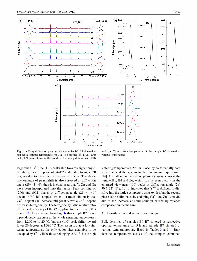
larger than Ti4?, the (110) peaks shift towards higher angle.
Similarly, the (110) peaks of B4–B7 tend to shift to higher 2hdegrees due to the effect of oxygen vacancies. The above
phenomenon of peaks shift is also observed at diffraction
angle (2h) 44–46�, thus it is concluded that Y, Zn and Ga
have been incorporated into the lattice. Peak splitting of
(200) and (002) planes at diffraction angle (2h) 44–46�occurs in B0–B5 samples, which illustrates obviously that
Ga3? dopant can increase tetragonality while Zn2? dopant
decreases tetragonality. The tetragonality is the relative ratio
of the peak intensity of the (200) plane to that of the (002)
plane [23]. It can be seen from Fig. 1c that sample B7 shows
a pseudocubic structure at the whole sintering temperatures
from 1,260 to 1,420 �C, but the (110) peak shifts toward
lower 2h degrees at 1,380 �C. The reason is that at low sin-
tering temperatures, the only cation sites available to be
occupied by Y3? will be those belonging to Ba2?, but at high
sintering temperatures, Y3? will occupy preferentially both
sites that lead the system to thermodynamic equilibrium
[24]. A small amount of second phase Y2Ti2O7 occurs in the
sample B1, B4 and B6, which can be seen clearly in the
enlarged view near (110) peaks at diffraction angle (2h)
30.5–32� (Fig. 1b). It indicates that Y3? is difficult to dis-
solve into the lattice completely as its oxides, but the second
phase can be eliminated by codoping Ga3? and Zn2?, maybe
due to the increase of solid solution caused by valence
compensation mechanism.
3.2 Densification and surface morphology
Bulk densities of samples B0–B7 sintered at respective
optimal temperature for 3 h and sample B7 sintered at
various temperatures are listed in Tables 3 and 4. Bulk
densities-temperatures curves of the samples contained
Fig. 1 a X-ray diffraction patterns of the samples B0–B7 sintered at
respective optimal temperature for 3 h (line profiles of (110), (200)
and (002) peaks shown in the inset); b The enlarged view near (110)
peaks; c X-ray diffraction patterns of the sample B7 sintered at
various temperatures
J Mater Sci: Mater Electron (2014) 25:2905–2912 2907
123

Y3? are illustrated in Fig. 2. It can be seen from Tables 3,
4 and Fig. 2 that Y2O3 dopant lead higher densification
temperature of BaTiO3 ceramics, the densification tem-
perature of B1 and B4 sample is 1,380 �C, while the
densification temperature of B6 and B7 sample is 1,340 �C.
However, bulk densities of Zn2? (B2) and Ga3? (B3)
doped samples can reach saturation at a lower temperature
(1,260 �C). It indicates that ZnO and Ga2O3 can improve
densification and decrease sintering temperature of doped
BaTiO3, which can be attributed to valence compensation
mechanism and changes in the mass caused by atomic
replacement. According to Kr}oger–Vink notation, the
possible defect equations are provided as follows:
Y2O3 ! 2Y�Ba þ 1=2V00Ti þ 3OO ð1Þ
Ga2O3 ! 2Ga0Ti þ V�O þ 3OO ð2Þ
ZnO ! Zn00Ti þ V��O þ OO ð3Þ
Y2O3 þ Ga2O3 ! 2Y�Ba þ 2Ga0Ti þ 6OO ð4Þ
Y2O3 þ ZnO ! 2Y�Ba þ Zn00Ti þ 4OO ð5Þ
2Y2O3 ! 2Y�Ba þ 2Y0Ti þ 6OO ð6Þ
The above valence compensation reaction (4)–(6) can
reduce excessive oxygen vacancies and improve sintering.
Densification can also be reflected from SEM images of the
sample fracture surface in Fig. 3. Morphology of
inhomogeneous grains with wide grain size distributions is
observed for B0 sample illustrated in Fig. 3a. The Y3?
doped sample (B1) sintered at 1,380 �C has an obvious
abnormal grain growth phenomenon shown in Fig. 3b,
maybe due to the high sintering temperature. It can be seen
from Fig. 3c, d, f that Zn2? and Ga3? can suppress the
grain growth in different degrees. It is known that the
incorporation of Zn2? and Ga3? will bring about plenty of
oxygen vacancies. The formation of oxygen vacancies can
lead to lattice distortion and ions located in the grain
boundary, which baffles motion of the grain boundary and
accordingly inhibits grain growth [25]. Compared with
single Y3? doped sample, Y3? and Ga3? codoped sample
shows a much smaller grain size distribution (Fig. 3e). The
Y/Zn codoped sample (B6) and Y/Zn/Ga codoped sample
(B7) sintered at 1,340 �C have similar micromorphology
with reasonably good close packing of grains and high
uniformity. Porous structure occurred in higher sintering
temperature for B7 sample (Fig. 3h, j).
3.3 Core–shell microstructures
Figure 4 shows the TEM micrographs of BaTiO3 codoped
with Y/Zn/Ga sintered at 1,340 �C for 3 h. Core–shell
structure is clearly revealed by the bright field image of
Fig. 4a and the evident interface between core and shell
Table 2 The results of XRD analyses from Fig. 1
Specimen Dopants (002) (200) Peaks Crystal structure (110) Peak shift toward Main mechanism
B0 / Splitting Tetragonal Lower 2h angle Ionic substitution
B1 Y Splitting Orthorhombic Higher 2h angle Oxygen vacancies
B2 Zn Splitting Tetragonal Higher 2h angle Oxygen vacancies
B3 Ga Splitting Tetragonal Higher 2h angle Oxygen vacancies
B4 Y/Ga Splitting Orthorhombic Higher 2h angle Oxygen vacancies
B5 Zn/Ga Splitting Tetragonal Higher 2h angle Oxygen vacancies
B6 Y/Zn No splitting Pseudocubic Higher 2h angle Oxygen vacancies
B7 Y/Zn/Ga No splitting Pseudocubic Higher 2h angle Oxygen vacancies
Table 3 Bulk densities and dielectric properties of specimen sintered at respective optimal temperature
Specimen Bulk density (g/cm3) Permittivity Dielectric loss Max|DC/C25| (%) BDV (kv/mm)
B0 1,260 �C 5.70 3,765 0.019 47.89 3.02
B1 1,380 �C 5.60 2,627 0.017 25.19 3.63
B2 1,260 �C 5.73 2,367 0.004 25.94 4.21
B3 1,260 �C 5.71 1,359 0.013 382.76 0.73
B4 1,340 �C 5.49 2,179 0.013 21.10 4.03
B5 1,260 �C 5.69 2,502 0.004 21.94 4.40
B6 1,340 �C 5.70 2,851 0.010 14.98 3.47
B7 1,340 �C 5.73 2,690 0.010 14.90 3.73
2908 J Mater Sci: Mater Electron (2014) 25:2905–2912
123

under HRTEM (High-Resolution TEM) in Fig. 4b. The
selected area electron-diffraction patterns from the core
shown in Fig. 4c indicate that an orthorhombic structure
(lattice parameter a = *4.0 A, c = *5.6 A) is formed.
The HRTEM lattice spacing measured in Fig. 4b also
confirms this. It can be seen from the results of EDS line
profile analysis in Fig. 4d that the concentrations of Y, Zn
and Ga are preserved to a certain depth from the grain
boundary and decrease toward the core region. So it is
apparent that Y3?, Zn2? and Ga3? can be dissolved into the
grains together, segregated at grain boundaries and play a
significant role in the formation of core–shell structure in
BaTiO3 ceramics.
3.4 Dielectric properties
Dielectric properties of samples sintered at respective
optimal temperature and sample B7 sintered at various
temperatures are listed in Tables 3 and 4, respectively. B0
sample possesses maximum room temperature permittivity
(*3,765) due to tetragonal structure and the contribution
of 90� domain walls determined by the grain size [26].
However, B3 sample with small grain size has low room
temperature permittivity in spite of tetragonal structure.
Other samples have the permittivity between 2,000 and
3,000, owe to the decrease in ionic polariability of the
dipole moment. According to Shannon’s conclusion about
ion polarizabilities [27], the values of a (Y3?) and a (Zn2?)
are 3.84 and 2.09 A3, respectively, smaller than a (Ba2?)
(6.4 A3) and a (Ti4?) (2.94 A3). In addition, permittivity
depends on the number of ion polarization in unit volume
[28], which can be decided by the bulk densities in a
degree. Thus the sample B7 sintered at 1,340 �C has the
max permittivity in the range of temperatures from 1,260 to
1,420 �C.
It is noticed that the Zn2? doped sample has the lowest
dielectric loss among all the samples. Sua et al. reported
the probable mechanism of dielectric loss influenced by
Mg2?. Mg2? can replace Ti4? as an acceptor for BaTiO3
with a double ionized oxygen vacancy (VO••) formed
simultaneously. Charged oxygen vacancies, in combination
with Mg2?, obviously lead to the local deformation of
perovskite unit cells. Thus, both electric dipoles formed
from MgTi00-VO
•• complex and elastic dipoles due to dis-
tortions caused by Vo•• will be present in the BaTiO3
ceramics. Oxygen vacancies in BaTiO3 reside at the cor-
ners of octahedral, are well interconnected, and can
therefore be regarded as relatively ‘‘mobile’’. Mobile defect
complexes migrate to domain boundaries. Orientation of
the electric and elastic dipoles results in domain-wall
pinning and thus a reduction of the dissipation in the fer-
roelectric state [29]. Since Zn2? and Mg2? have the similar
ionic radius and valence shell structure, thus we take it for
granted that the above mechanism can also be applied to
Zn2?. Moreover, Zn2? doped sample with low tand can be
partly attributed to the well-densified structure without any
visible pores and cracks. It can be seen from the Table 3
that Y3? and Ga3? have no obvious effect on the dielectric
loss.
Figure 5 shows temperature coefficient of capacitance
(TCC) curves of the samples sintered at respective optimal
temperature for 3 h. The curves of samples with tetragonal
phase exhibit a sharp peak at Curie temperature
(Tc & 125 �C), which is caused by tetragonal-to-cubic
phase transition. The Curie peak increases as the tetrago-
nality increases. The other doped groups exhibit relatively
Table 4 Bulk densities and
dielectric properties of
specimen B7 sintered at various
temperatures
Sintering
temperature
Bulk density
(g/cm3)
Permittivity Dielectric loss Max|DC/C25| (%) BDV
(kv/mm)
1,260 5.51 2,323 0.013 14.89 3.79
1,300 5.64 2,521 0.012 17.44 3.46
1,340 5.73 2,690 0.010 14.90 3.73
1,380 5.69 2,608 0.011 19.83 3.27
1,420 5.69 2,677 0.017 25.33 2.40
Fig. 2 Bulk densities-temperatures curves of samples B1, B4, B6 and
B7
J Mater Sci: Mater Electron (2014) 25:2905–2912 2909
123

Fig. 3 SEM of the fracture
surface of BaTiO3 samples:
a B0 sintered at 1,260 �C, b B1
at 1,380 �C, c B2 at 1,260 �C,
d B3 at 1,260 �C, e B4 at
1,340 �C, f B5 at 1,260 �C,
g B6 at 1,340 �C, h B7 at
1,380 �C, i B7 at 1,340 �C, j B7
at 1,420 �C
2910 J Mater Sci: Mater Electron (2014) 25:2905–2912
123

stable characteristics through the entire temperatures from
-55 to 125 �C. Among these samples, B6 and B7 samples
exhibit the best TCC characterization, meet the EIA-X7R
requirements that keep the max|DC/C25|under 15 %. The
capacitance–temperature stability characteristics are asso-
ciated with the core–shell structure. The dopants Y3?, Zn2?
and Ga3? can diffuse into BaTiO3 grains to a certain depth
collectively to form the shell of pseudocubic phase, and
lead to the volume fraction of grain core decreasing. Thus,
the sharp dielectric peak at Tc is depressed distinctly and
becomes widely broad.
The AC voltage resistance characteristics show no
obvious regularity among these samples. All samples can
improve the AC voltage resistance characteristics com-
pared with the undoped one except for Ga3? single-doped
sample. It indicates that the AC resistance characteristics
decrease with the increase in tetragonality. In addition, it is
believed that AC Breakdown Voltage (BDV) is related to
doped elements, amount of dopants, sintering temperature,
and etc. It is also believed that dielectric loss, grain size, as
well as frequency of closed pores, are the factors to affect
AC breakdown field strength [30].
4 Conclusions
In the paper, the doping behaviors of yttrium, zinc and
gallium and their effects on the dielectric properties and
microstructures of BaTiO3 were investigated. Y3? dis-
solved into the lattice of BaTiO3, and replaced both Ba2?
site and Ti4? site; while Zn2? and Ga3? tended to occupy
Ti4? site. Compared with Y2O3 and Ga2O3, ZnO sup-
pressed grain growth of BaTiO3 more effectively and
Fig. 4 a TEM bright field image, b HRTEM (High-Resolution TEM), c selected area electron-diffraction patterns from the core of core–shell
structure, and d EDS line profile for the core–shell grain of B7 sample sintered at 1,340 �C
Fig. 5 Temperature coefficient of capacitance (C - C25)/C25 of the
samples B0–B7 sintered at each own optimal temperature for 3 h
J Mater Sci: Mater Electron (2014) 25:2905–2912 2911
123

promoted greater uniformity of grains, thus reducing the
dielectric loss. Ga2O3 was conducive to the formation of
pure phase and improved sintering, which was ascribed to
the compensation mechanism and synergistic effect. The
formation of core–shell structure led to the dielectric
temperature characteristics improving by codoping proper
amount of Y2O3, Ga2O3 and ZnO. BaTiO3-0.025Y2O3-
0.025ZnO-0.01Ga2O3-0.01.
SiO2 ceramics sintered at 1,340 �C exhibit the best
dielectric properties: er = 2,690, tand = 1.0 % (at 1 kHz),
DC/C25 \*15 % (from -55 to 125 �C) and AC break-
down voltage E [ 3.73 kV/mm. This material has a
potential application in AC multilayer ceramic capacitor.
References
1. S.J. Fiedziuszko, I.C. Hunter, T. Itoh, Y. Kobayashi, T. Nishik-
awa, S.N. Stitzer, K. Wakino, IEEE Trans. Microw. Theory Tech.
50, 706–720 (2002)
2. H. Kishi, Y. Mizuno, H. Chazono, Jpn. J. Appl. Phys. 42, 1–15
(2003)
3. T.V. Tarasevich, S.A. Lebedev, S.A. Filatov, Inorg. Mater. 46,
237–241 (2010)
4. X. Ning, P.Y. Ping, W. Zhuo, J. Am. Ceram. Soc. 95, 999–1003
(2012)
5. H.E. Kim, S.M. Choi, S.Y. Lee, Y.W. Hong, S.I. Yoo, Electron.
Mater. Lett. 9, 325–330 (2013)
6. S.H. Wu, S. Wang, L.Y. Chen, X.Y. Wang, J. Mater. Sci Mater.
Electron. 19, 505–508 (2008)
7. L.X. Li, Y.M. Han, P. Zhang, C. Ming, X. Wei, J. Mater. Sci. 44,
5563–5568 (2009)
8. S. Wang, H. He, H. Su, J. Mater. Sci. Mater. Electron. 23,
1875–1880 (2012)
9. I. Fujii, S. Trolier-McKinstry, C. Nies, J. Am. Ceram. Soc. 94,
194–199 (2011)
10. S.F. Wang, G.O. Dayton, J. Am. Ceram. Soc. 82, 2677–2682 (1999)
11. S.C. Jeon, C.S. Lee, S.J.L. Kang, J. Am. Ceram. Soc. 95,
2435–2438 (2012)
12. H. Kishi, N. Kohzu, J. Sugino, H. Ohsato, Y. Iguchi, T. Okuda, J.
Eur. Ceram. Soc. 19, 1043–1046 (1999)
13. U. Syamaprasad, A.R.S. Nair, M.S. Sarma, P. Guruswamy, P.S.
Mukherjee, A.D. Damodaran, L. Krishnamurth, M. Achuthan, J.
Mater. Sci. Mater. Electron. 8, 199–205 (1997)
14. C.Y. Chang, W.N. Wang, C.Y. Huang, J. Am. Ceram. Soc. 96,
2570–2576 (2013)
15. B. Li, S.R. Zhang, X.H. Zhou, Z. Chen, S. Wang, J. Mater. Sci.
42, 5223–5228 (2007)
16. S. Sato, Y. Nakano, A. Sato, T. Nomura, J. Eur. Ceram. Soc. 19,
1061–1065 (1999)
17. Y.C. Lee, C.W. Lin, WHLu Int, J. Appl. Ceram. Technol. 6,
692–701 (2009)
18. Q. Zhou, C.R. Zhou, H.B. Yang, C.L. Yuan, G.H. Chen, L. Cao,
Q.L. Fan, J. Mater. Sci. Mater. Electron. 25, 196–201 (2014)
19. D. Gulwade, P. Gopalan, Phys. B 404, 1799–1805 (2009)
20. R.D. Shannon, Acta Crystallogr. A 32, 751–767 (1976)
21. J. Zhi, A. Chen, Y. Zhi, P.M. Vilarinho, J.L. Baptista, J. Am.
Ceram. Soc. 82, 1345–1348 (1999)
22. X.T. Li, W.L. Huo, W.J. Weng, G.R. Han, P.Y. Du, J. Electro-
ceram. 21, 128–131 (2008)
23. D.W. Kang, T.G. Park, J.W. Kim, J.S. Kim, H.S. Lee, H. Cho,
Electron. Mater. Lett. 6, 145–149 (2010)
24. M. Paredes-Olguın, I.A. Lira-Hernandez, C. Gomez-Yanez, F.P.
Espino-Cortes, Phys. B 410, 157–161 (2013)
25. W. Cai, C.L. Fu, J.C. Gao, C.X. Zhao, Adv. Appl. Ceram. 110,
181–185 (2011)
26. G. Arlt, D. Hennings, G. de With, J. Appl. Phys. 58, 1619–1624
(1985)
27. R.D. Shannon, J. Appl. Phys. 73, 348–366 (1993)
28. Y.C. Chen, J. Alloys Compd. 527, 84–89 (2012)
29. B. Sua, T.W. Button, J. Appl. Phys. 95, 1382–1385 (2004)
30. G.H. Maher, J.M. Wilson, S.G. Maher, Carts-conference, USA,
(2006)
2912 J Mater Sci: Mater Electron (2014) 25:2905–2912
123