dominant tm opto technologies mini domiled …€¦ · rel forward current i f (ma) temperature...
TRANSCRIPT

1
Features:> High brightness surface mount LED.> 120° viewing angle.> Small package outline (LxWxH) of 2.0 x 1.4 x 1.3mm.> Qualified according to JEDEC moisture sensitivity Level 2.> Compatible to IR reflow soldering.> Environmental friendly; RoHS compliance.> Compliance to automotive standard; AEC-Q101.> Passed Corrosion Resistant Test. Appx. 4.1
Mini DomiLEDSynonymous with function and performance, the Mini DomiLED series is perfectly suited for a variety of cross-industrial applications due to its small package outline, durability and superior brightness.
DATA SHEET:
Mini DomiLEDAlInGaP : DLx-HJS
© 2005 DomiLED is a trademark of DOMINANT Opto Technologies.All rights reserved. Product specifications are subject to change without notice.
Applications:> Automotive: interior applications, eg: switches, telematics, climate control system, dashboard, etc.> Signage: full color display video notice board, signage, special effect lighting> Lighting: channel light
DOMINANTOpto TechnologiesInnovating Illumination
TM
20/06/2017 V3.0

2
DLS-HJS-UV1-1
DLR-HJS-U2V-1
DLA-HJS-VW1-1
DLO-HJS-VW1-1
DLY-HJS-UV2-1
Super Red, 632nm
Red, 620nm
Amber, 615nm
Orange, 605nm
Yellow, 590nm
120
120
120
120
120
450.0
560.0
715.0
715.0
450.0
Part OrderingNumber
Color ViewingAngle˚
Luminous Intensity @ IF = 20mA IV (mcd) Appx. 1.1
Optical Characteristics at Tj=25˚C
Min. Typ. Max.
560.0
715.0
1125.0
1125.0
715.0
900.0
1125.0
1400.0
1400.0
1125.0
Typ. (V)Vf @ If = 20mA Appx 3.1
Electrical Characteristics at Tj=25˚C
Max. (V)Vr @ Ir = 10uA
Min. (V)Part Number
DLx-HJS 2.1 2.41.8
Min. (V)
12
Unit
Absolute Maximum Ratings
Maximum Value
DC forward current
Peak pulse current; (tp ≤ 10µs, Duty cycle = 0.005)
Reverse voltage
ESD threshold (HBM)
LED junction temperature
Operating temperature
Storage temperature
Power dissipation (at room temperature)
Thermal resistance- Real Thermal Resistance Junction / ambient, Rth JA real Junction / solder point, Rth JS real - Electrical Thermal Resistance Junction / ambient, Rth JA el Junction / solder point, Rth JS el(Mounting on FR4 PCB, pad size >= 16 mm2 per pad)
50
100
12
2000
125
-40 … +100
-40 … +100
125
440200
360160
mA
mA
V
V
˚C
˚C
˚C
mW
K/WK/W
K/WK/W
20/06/2017 V3.0
AllnGaP : DLx-HJSDOMINANTOpto TechnologiesInnovating Illumination
TM

Optical Characteristics at Tj=25˚C
3
Group
Wavelength Grouping at Tj=25˚CWavelength distribution (nm) Appx. 2.2Color
DLS; Super Red
DLR; Red
DLA; Amber
DLO; Orange
DLY; Yellow
Full
Full
FullWX
FullWXYZ
FullXYZ
625 - 640
620 - 630
610 - 621610 - 615615 - 621
600 - 612600 - 603603 - 606606 - 609609 - 612
585 - 594585 - 588588 - 591591 - 594
20/06/2017 V3.0
AllnGaP : DLx-HJSDOMINANTOpto TechnologiesInnovating Illumination
TM

4 20/06/2017 V3.0
U1U2V1V2W1
450.0 ... 560.0560.0 ... 715.0715.0 ... 900.0900.0 ... 1125.0
1125.0 ... 1400.0
Brightness Group Luminous Intensity Appx. 1.1
IV (mcd)
Luminous Intensity Group at Tj=25˚C
Group Wavelength distribution (nm)Forward Voltage (V) Appx. 3.1
Vf Binning (Optional)
Vf Bin @ 20mA
VA
VB
VC
VD
1.80 ... 1.95
1.95 ... 2.10
2.10 ... 2.25
2.25 ... 2.40
Please consult sales and marketing for special part number to incorporate Vf binning.
AllnGaP : DLx-HJSDOMINANTOpto TechnologiesInnovating Illumination
TM

5 20/06/2017 V3.0
AllnGaP : DLx-HJSDOMINANTOpto TechnologiesInnovating Illumination
TM
Forw
ard
Cur
rent
I F (m
A)
Rel
ativ
e Lu
min
ous
Inte
nsity
I rel
Forw
ard
Cur
rent
I F (m
A)
Temperature T(°C)
Rel
ativ
e Lu
min
ous
Inte
nsity
I rel
Wavelength λ (nm)
Allo
wab
le F
orw
ard
Cur
rent
I F( m
A )
Duty Ratio, %
Allowable Forward Current Vs Duty Ratio ( Tj = 25°C; tp ≤ 10μs)
Radiation Pattern
Forward Current IF (mA)
Relative Luminous Intensity Vs Forward CurrentIV/IV(20mA) = f(IF); Tj = 25°C
Forward Current Vs Forward VoltageIF = f(VF); Tj = 25°C
Forward Voltage VF (V)
Maximum Current Vs TemperatureIF=f(T)
Relative Spectral EmissionIrel = f(λ); Tj = 25°C; IF = 20mA
08/12/2016 V7.09
InGaN Warm White: DDF-LJGDOMINANTOpto TechnologiesInnovating Illumination
TM
Radiation Pattern
Junction Temperature Tj(°C)
Rel
ativ
e Fo
rwar
d Vo
ltage
∆V F (
V)
Junction Temperature Tj(°C)
Rel
ativ
e Lu
min
ous
Inte
nsity
I rel
Relative Luminous Intensity Vs Junction TemperatureIV/IV(25°C) = f(Tj); IF = 20mA
Junction Temperature Tj(°C)
∆Cx
, ∆C
y
Chromaticity Coordinate Shift Vs Junction Temperature∆Cx, ∆Cy = f(Tj); IF = 20mA
0.270°
90°
80°
0
60°
50°
40°
30° 20°
0.6
0.4
1.0
0.8
10° 0°
-0.5
-0.4
-0.3
-0.2
-0.1
0.0
0.1
0.2
0.3
0.4
0.5
-50 -30 -10 10 30 50 70 90 110 1300.0
0.2
0.4
0.6
0.8
1.0
1.2
1.4
1.6
1.8
2.0
-50 -30 -10 10 30 50 70 90 110 130
Rela
tive
Forw
ard
Volta
ge ∆
V F (V
)
Relative Forward Voltage Vs Junction Temperature∆VF = VF - VF(25°C) = f(Tj); IF = 20mA
Junction Temperature Tj(°C) Junction Temperature Tj(°C)
Relative Luminous Intensity Vs Junction TemperatureIV /IV (25°C) = f(Tj); IV = 20mA
Rela
tive
Lum
inou
s In
tens
ity I r
el
Relative Forward Voltage Vs Junction Temperature∆VF = VF - VF(25°C) = f(Tj); IF =20mA
-10.0
-8.0
-6.0
-4.0
-2.0
0.0
2.0
4.0
6.0
8.0
10.0
-50 -30 -10 10 30 50 70 90 110 130
∆Cx
∆Cy
-0.030
-0.025
-0.020
-0.015
-0.010
-0.005
0.000
0.005
0.010
0.015
0.020
0.025
0.030
-50 -30 -10 10 30 50 70 90 110 130
Rela
tive
Wav
elen
gth ∆λ
dom
(nm
)
Relative Wavelength Vs Junction Temperature∆λdom = λdom - λdom (25°C) = f(Tj); IF = 20mA
∆Cx,
∆Cy
Chromaticity Coordinate Shift Vs Junction Temperature∆Cx, ∆Cy = f(Tj); IF = 20mA
Junction Temperature Tj(°C) Junction Temperature Tj(°C)
0.0
0.5
1.0
1.5
2.0
2.5
0 5 10 15 20 25 30 35 40 45 500
5
10
15
20
25
30
35
40
45
50
1.7 1.8 1.9 2.0 2.1 2.2 2.3 2.4 2.5
Forw
ard
Cur
rent
I F
Forward Current IF (mA)
Forward Current Vs Forward VoltageIF = f(VF); Tj = 25°C
Forward Voltage VF (V)
0.0
0.1
0.2
0.3
0.4
0.5
0.6
0.7
0.8
0.9
1.0
450 500 550 600 650 700 750 800
Wavelength λ (nm)
Forw
ard
Cur
rent
I F(m
A)
Maximum Current Vs TemperatureIF = f (T)
Temperature T(°C)
TA
TS
0
10
20
30
40
50
60
0 10 20 30 40 50 60 70 80 90 100 110
TA = Ambient TemperatureTS = Solder Point Temperature
Allo
wab
le F
orw
ard
Cur
rent
I F (
mA
)
Allowable Forward Current Vs Duty Ratio ( Tj = 25°C; tp ≤ 10μs )
Duty Ratio, %
10
100
1000
0.1 1 10 100
Rel
ativ
e Lu
min
ous
Inte
nsity
I rel
Rel
ativ
e Lu
min
ous
Inte
nsity
I rel
Relative Luminous Intensity Vs Forward CurrentIV/IV(20mA) = f(IF); Tj = 25°C
Relative Spectral EmissionIrel = f(λ); Tj = 25°C; IF = 20mA
YellowRed
Amber
Super RedOrange
0.0
0.5
1.0
1.5
2.0
2.5
0 5 10 15 20 25 30 35 40 45 500
5
10
15
20
25
30
35
40
45
50
1.7 1.8 1.9 2.0 2.1 2.2 2.3 2.4 2.5
Forw
ard
Cur
rent
I FForward Current IF (mA)
Forward Current Vs Forward VoltageIF = f(VF); Tj = 25°C
Forward Voltage VF (V)
0.0
0.1
0.2
0.3
0.4
0.5
0.6
0.7
0.8
0.9
1.0
450 500 550 600 650 700 750 800
Wavelength λ (nm)
Forw
ard
Cur
rent
I F(m
A)
Maximum Current Vs TemperatureIF = f (T)
Temperature T(°C)
TA
TS
0
10
20
30
40
50
60
0 10 20 30 40 50 60 70 80 90 100 110
TA = Ambient TemperatureTS = Solder Point Temperature
Allo
wab
le F
orw
ard
Cur
rent
I F (
mA
)
Allowable Forward Current Vs Duty Ratio ( Tj = 25°C; tp ≤ 10μs )
Duty Ratio, %
10
100
1000
0.1 1 10 100
Rel
ativ
e Lu
min
ous
Inte
nsity
I rel
Rel
ativ
e Lu
min
ous
Inte
nsity
I rel
Relative Luminous Intensity Vs Forward CurrentIV/IV(20mA) = f(IF); Tj = 25°C
Relative Spectral EmissionIrel = f(λ); Tj = 25°C; IF = 20mA
YellowRed
Amber
Super RedOrange
0.0
0.5
1.0
1.5
2.0
2.5
0 5 10 15 20 25 30 35 40 45 500
5
10
15
20
25
30
35
40
45
50
1.7 1.8 1.9 2.0 2.1 2.2 2.3 2.4 2.5
Forw
ard
Cur
rent
I F
Forward Current IF (mA)
Forward Current Vs Forward VoltageIF = f(VF); Tj = 25°C
Forward Voltage VF (V)
0.0
0.1
0.2
0.3
0.4
0.5
0.6
0.7
0.8
0.9
1.0
450 500 550 600 650 700 750 800
Wavelength λ (nm)
Forw
ard
Cur
rent
I F(m
A)
Maximum Current Vs TemperatureIF = f (T)
Temperature T(°C)
TA
TS
0
10
20
30
40
50
60
0 10 20 30 40 50 60 70 80 90 100 110
TA = Ambient TemperatureTS = Solder Point Temperature
Allo
wab
le F
orw
ard
Cur
rent
I F (
mA
)
Allowable Forward Current Vs Duty Ratio ( Tj = 25°C; tp ≤ 10μs )
Duty Ratio, %
10
100
1000
0.1 1 10 100
Rel
ativ
e Lu
min
ous
Inte
nsity
I rel
Rel
ativ
e Lu
min
ous
Inte
nsity
I rel
Relative Luminous Intensity Vs Forward CurrentIV/IV(20mA) = f(IF); Tj = 25°C
Relative Spectral EmissionIrel = f(λ); Tj = 25°C; IF = 20mA
YellowRed
Amber
Super RedOrange
0.0
0.5
1.0
1.5
2.0
2.5
0 5 10 15 20 25 30 35 40 45 500
5
10
15
20
25
30
35
40
45
50
1.7 1.8 1.9 2.0 2.1 2.2 2.3 2.4 2.5Fo
rwar
d C
urre
nt I F
Forward Current IF (mA)
Forward Current Vs Forward VoltageIF = f(VF); Tj = 25°C
Forward Voltage VF (V)
0.0
0.1
0.2
0.3
0.4
0.5
0.6
0.7
0.8
0.9
1.0
450 500 550 600 650 700 750 800
Wavelength λ (nm)
Forw
ard
Cur
rent
I F(m
A)
Maximum Current Vs TemperatureIF = f (T)
Temperature T(°C)
TA
TS
0
10
20
30
40
50
60
0 10 20 30 40 50 60 70 80 90 100 110
TA = Ambient TemperatureTS = Solder Point Temperature
Allo
wab
le F
orw
ard
Cur
rent
I F (
mA
)
Allowable Forward Current Vs Duty Ratio ( Tj = 25°C; tp ≤ 10μs )
Duty Ratio, %
10
100
1000
0.1 1 10 100
Rel
ativ
e Lu
min
ous
Inte
nsity
I rel
Rel
ativ
e Lu
min
ous
Inte
nsity
I rel
Relative Luminous Intensity Vs Forward CurrentIV/IV(20mA) = f(IF); Tj = 25°C
Relative Spectral EmissionIrel = f(λ); Tj = 25°C; IF = 20mA
YellowRed
Amber
Super RedOrange
0.0
0.5
1.0
1.5
2.0
2.5
0 5 10 15 20 25 30 35 40 45 500
5
10
15
20
25
30
35
40
45
50
1.7 1.8 1.9 2.0 2.1 2.2 2.3 2.4 2.5
Forw
ard
Cur
rent
I F
Forward Current IF (mA)
Forward Current Vs Forward VoltageIF = f(VF); Tj = 25°C
Forward Voltage VF (V)
0.0
0.1
0.2
0.3
0.4
0.5
0.6
0.7
0.8
0.9
1.0
450 500 550 600 650 700 750 800
Wavelength λ (nm)
Forw
ard
Cur
rent
I F(m
A)
Maximum Current Vs TemperatureIF = f (T)
Temperature T(°C)
TA
TS
0
10
20
30
40
50
60
0 10 20 30 40 50 60 70 80 90 100 110
TA = Ambient TemperatureTS = Solder Point Temperature
Allo
wab
le F
orw
ard
Cur
rent
I F (
mA
)
Allowable Forward Current Vs Duty Ratio ( Tj = 25°C; tp ≤ 10μs )
Duty Ratio, %
10
100
1000
0.1 1 10 100
Rel
ativ
e Lu
min
ous
Inte
nsity
I rel
Rel
ativ
e Lu
min
ous
Inte
nsity
I rel
Relative Luminous Intensity Vs Forward CurrentIV/IV(20mA) = f(IF); Tj = 25°C
Relative Spectral EmissionIrel = f(λ); Tj = 25°C; IF = 20mA
YellowRed
Amber
Super RedOrange
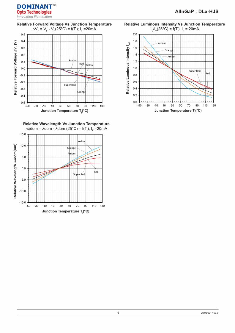
6 20/06/2017 V3.0
AllnGaP : DLx-HJSDOMINANTOpto TechnologiesInnovating Illumination
TM
Junction Temperature Tj(°C)
Rel
ativ
e Fo
rwar
d Vo
ltage
∆V F (
V)
Relative Forward Voltage Vs Junction Temperature∆VF = VF - VF(25°C) = f(Tj); IF =20mA
Junction Temperature Tj(°C)
Rel
ativ
e Lu
min
ous
Inte
nsity
I rel
Relative Luminous Intensity Vs Junction TemperatureIV/IV(25°C) = f(Tj); IF = 20mA
Junction Temperature Tj(°C)
Rel
ativ
e W
avel
engt
h ∆λ
dom
(nm
)
Relative Wavelength Vs Junction Temperature∆λdom = λdom - λdom (25°C) = f(Tj); IF =20mA
-0.5
-0.4
-0.3
-0.2
-0.1
0.0
0.1
0.2
0.3
0.4
0.5
-50 -30 -10 10 30 50 70 90 110 130
Super Red
0.0
0.2
0.4
0.6
0.8
1.0
1.2
1.4
1.6
1.8
2.0
-50 -30 -10 10 30 50 70 90 110 130
Rel
ativ
e Fo
rwar
d Vo
ltage
∆V F
(V)
Relative Forward Voltage Vs Junction Temperature∆VF = VF - VF(25°C) = f(Tj); IF =20mA
Junction Temperature Tj(°C) Junction Temperature Tj(°C)
Rel
ativ
e Lu
min
ous
Inte
nsity
I rel
Relative Luminous Intensity Vs Junction TemperatureIV /IV (25°C) = f(Tj); IV = 20mA
YellowRedAmber
Yellow
Red
Amber
Super Red
Orange
Orange
-15.0
-10.0
-5.0
0.0
5.0
10.0
15.0
-50 -30 -10 10 30 50 70 90 110 130
∆Cx
∆Cy
-0.05
-0.04
-0.03
-0.02
-0.01
0.00
0.01
0.02
0.03
0.04
0.05
-50 -30 -10 10 30 50 70 90 110
Rel
ativ
e W
avel
engt
h ∆λ
dom
(nm
)
Relative Wavelength Vs Junction Temperature∆λdom = λdom - λdom (25°C) = f(Tj); IF = 20mA
∆Cx,
∆C
y
Chromaticity Coordinate Shift Vs Junction Temperature∆Cx, ∆Cy = f(Tj); IF = 5mA
Junction Temperature Tj(°C) Junction Temperature Tj(°C)
Yellow
Red
Amber
Super Red
Orange

7
Mini DomiLED • AllnGaP : DLx-HJS Package Outlines
Material
Material
Lead-frame
Package
Encapsulant Soldering Leads
Cu Alloy With Ag Plating
High Temperature Resistant Plastic, PPA
Epoxy
Sn-Sn Plating
20/06/2017 V3.0
Notes: Primary thermal path is through Anode lead of LED package
AllnGaP : DLx-HJSDOMINANTOpto TechnologiesInnovating Illumination
TM

8
Recommended Solder Pad
20/06/2017 V3.0
AllnGaP : DLx-HJSDOMINANTOpto TechnologiesInnovating Illumination
TM

9
Taping and orientation
• Reels come in quantity of 3000 units.• Reel diameter is 180 mm.
20/06/2017 V3.0
AllnGaP : DLx-HJSDOMINANTOpto TechnologiesInnovating Illumination
TM

10
Packaging Specification
20/06/2017 V3.0
AllnGaP : DLx-HJSDOMINANTOpto TechnologiesInnovating Illumination
TM
08/12/2016 V7.013
Packaging Specification
InGaN Warm White: DDF-LJGDOMINANTOpto TechnologiesInnovating Illumination
TM

11 20/06/2017 V3.0
Packaging Specification
Average 1pc Mini DomiLED 1 completed bag (3000pcs)
0.034 190 ± 10Weight (gram)
CardboardBox
Dimensions (mm) Empty BoxWeight (kg)
Super Small
Small
Medium
Large
For Mini DomiLED
Reel / BoxCardboard BoxSize
Weight (gram) 0.007 200 ± 10
DOMINANT TM
Moisture sensitivity level
Moisture absorbent material +Moisture indicator
The reel, moisture absorbent material and moisture indicator aresealed inside the moisture proof foil bag
Reel
Barcode label
Label
(L) Lot No : lotno
(P) Part No : partno
(C) Cust No : partno
(G) Grouping : group
(Q) Quantity : quantity
(D) D/C : date code
(S) S/N : serial no
DOMINANT Opto TechnologiesML TEMP2 260˚CRoHS Compliant
Made in Malaysia
325 x 225 x 190
325 x 225 x 280
570 x 440 x 230
570 x 440 x 460
0.38
0.54
1.46
1.92
9 reels MAX
15 reels MAX
60 reels MAX
120 reels MAX
AllnGaP : DLx-HJSDOMINANTOpto TechnologiesInnovating Illumination
TM

20/06/2017 V3.012
Time (sec)0 50 100 150 200
300
250
225
200
175
150
125
100
75
50
25
275
Tem
pera
ture
(˚C
)Classification Reflow Profile (JEDEC J-STD-020C)
Ramp-up3˚C/sec max.
255-260˚C10-30s
60-150s
Ramp-down
6˚C/secmax.
Preheat 60-180s
480s max
217˚C
Recommended Pb-free Soldering Profile
AllnGaP : DLx-HJSDOMINANTOpto TechnologiesInnovating Illumination
TM

20/06/2017 V3.013
AllnGaP : DLx-HJSDOMINANTOpto TechnologiesInnovating Illumination
TM
Appendix
1) Brightness:1.1 Luminous intensity is measured with an internal reproducibility of ± 8 % and an expanded uncertainty of ± 11 % (according to GUM with a coverage factor of k=3).1.2 Luminous flux is measured with an internal reproducibility of ± 8 % and an expanded uncertainty of ± 11 % (according to GUM with a coverage factor of k=3).
2) Color:2.1 Chromaticity coordinate groups are measured with an internal reproducibility of ± 0.005 and an expanded uncertainty of ± 0.01 (accordingly to GUM with a coverage factor of k=3).2.2 DOMINANT wavelength is measured with an internal reproducibility of ± 0.5nm and an expanded uncertainty of ± 1nm (accordingly to GUM with a coverage factor of k=3).
3) Voltage:3.1 Forward Voltage, Vf is measured with an internal reproducibility of ± 0.05V and an expanded uncertainty of ± 0.1V (accordingly to GUM with a coverage factor of k=3).
4) Corrosion Robustness:4.1 Test conditions: 40 °C / 90 % rh / 15 ppm H2S / 336 h. = Stricter than IEC 60068-2-43 (H2S) [25 °C / 75% rh / 10 ppm H2S / 21 days].

Revision History
Page
-
2, 4
2
Subjects
Initial Release
Update Vf Value
Add New Partno: DLO-HJS-VW1-1
Date of Modification
03 Nov 2016
28 Nov 2016
20 Jun 2017
14
NOTE
All the information contained in this document is considered to be reliable at the time of publishing. However, DOMINANT
Opto Technologies does not assume any liability arising out of the application or use of any product described herein.
DOMINANT Opto Technologies reserves the right to make changes to any products in order to improve reliability, function
or design.
DOMINANT Opto Technologies products are not authorized for use as critical components in life support devices or systems
without the express written approval from the Managing Director of DOMINANT Opto Technologies.
20/06/2017 V3.0
AllnGaP : DLx-HJSDOMINANTOpto TechnologiesInnovating Illumination
TM

About Us
DOMINANT Opto Technologies is a dynamic company that is amongst the world’s leading automotive LED manufac-turers. With an extensive industry experience and relentless pursuit of innovation, DOMINANT’s state-of-art manu-facturing and development capabilities have become a trusted and reliable brand across the globe. More information about DOMINANT Opto Technologies, a ISO/TS 16949 and ISO 14001 certified company, can be found under http://www.dominant-semi.com.
Please contact us for more information:
DOMINANT Opto Technologies Sdn. Bhd.Lot 6, Batu Berendam, FTZ Phase III, 75350 Melaka, MalaysiaTel: (606) 283 3566 Fax: (606) 283 0566E-mail: [email protected]
AllnGaP : DLx-HJSDOMINANTOpto TechnologiesInnovating Illumination
TM