doku modbus m3749 · v1.40 – 24.07.2019 page 4 1 general modbus information 1.1 documentation of...
TRANSCRIPT

M3749
Modbus implementation description
V1.40 – 24.07.2019 page 2
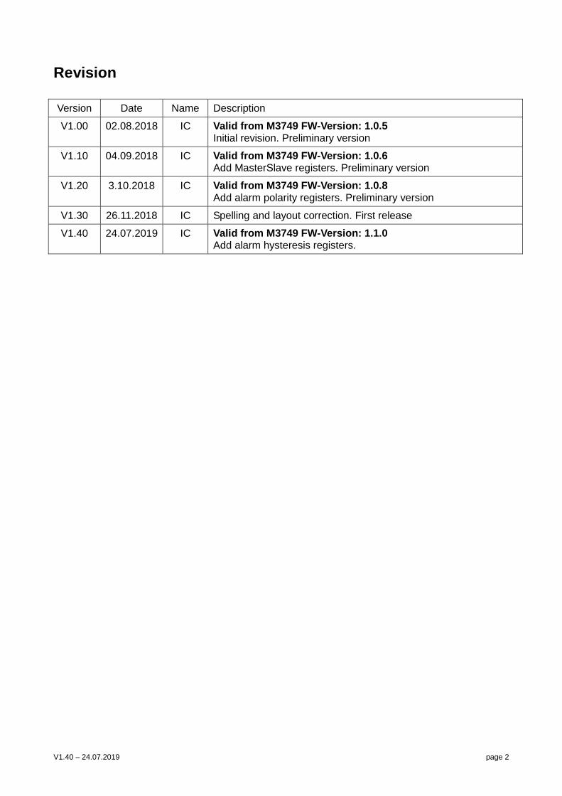
Revision
Version Date Name Description
V1.00 02.08.2018 IC Valid from M3749 FW-Version: 1.0.5 Initial revision. Preliminary version
V1.10 04.09.2018 IC Valid from M3749 FW-Version: 1.0.6 Add MasterSlave registers. Preliminary version
V1.20 3.10.2018 IC Valid from M3749 FW-Version: 1.0.8 Add alarm polarity registers. Preliminary version
V1.30 26.11.2018 IC Spelling and layout correction. First release
V1.40 24.07.2019 IC Valid from M3749 FW-Version: 1.1.0 Add alarm hysteresis registers.

V1.40 – 24.07.2019 page 3
Contents
1 General Modbus Information ................................................................................................... 4 1.1 Documentation of the Modbus protocol ......................................................................... 4 1.2 Modbus testing tool ....................................................................................................... 4 1.3 Protocol definitions, as implemented in M3749 ............................................................. 4 1.4 Modbus RTU function codes implemented in M3749 .................................................... 4 1.5 Data representation ...................................................................................................... 4 1.6 Addressing scheme ...................................................................................................... 5 1.7 Error handling ............................................................................................................... 5 1.8 User levels, Password protection .................................................................................. 6 1.9 Writing registers, data retention .................................................................................... 7
2 Implemented Modbus registers in the M3749 .......................................................................... 8 2.1 M3749 Modbus registers .............................................................................................. 8
3 Detailed description of the implemented Modbus registers .................................................... 14 3.1 Communication Setup Page ....................................................................................... 14
3.1.1 User levels and passwords ...................................................................................... 14 3.1.2 Modbus register offset ............................................................................................. 14 3.1.3 Configuration of the RS485 interface ....................................................................... 15

V1.40 – 24.07.2019 page 4
1 General Modbus Information
1.1 Documentation of the Modbus protocol
For detailed information about Modbus specifications, please refer to the following documents:
Modbus_over_serial_line_V1_02.pdf
Modbus_Application_Protocol_V1_1b3.pdf These documents are available on the Modbus website: www.modbus.org Go to tab „Technical Resources“.
1.2 Modbus testing tool
On the web, there are plenty of Modbus testing tools or Modbus libraries available for C++, Phyton or other programming languages. For manually accessing the M3749 over Modbus, for instance to predefine the Modbus address, baud rate, or other items, the tool „Modbus Poll“ is a feasible choice. It can be purchased at http://www.modbustools.com
1.3 Protocol definitions, as implemented in M3749
Modbus mode: RTU Start bits: 1 Data bits: 8 Stop bits: 1(default), 2 Parity: None (default), Odd, Even Baud rate: 4800, 9600, 19200, 38400(default), 57600, 115200 Device address: 1 (default) to 247
1.4 Modbus RTU function codes implemented in M3749
#3 Read Holding Registers #4 Read Input Registers #6 Write Single Register #16 Write Multiple Registers For detailed description of these functions please consult the document „Modbus_Application_Protocol_V1_1b3.pdf“. With the M3749, reading any register is performed by either command #3 or #4. There is no difference in handling the information between these two commands.
1.5 Data representation
Each Modbus register contains two bytes, the data length of a command and an answer is always a multiple of two registers. The high byte (first byte) of a register contains the last digit of a value or string, the first digit of a value or string is found on the low byte (second byte) of the last register of the interesting register chain. The first byte of a register always contains the higher order bits, the second byte contains the lower order bits.
V1.40 – 24.07.2019 page 5
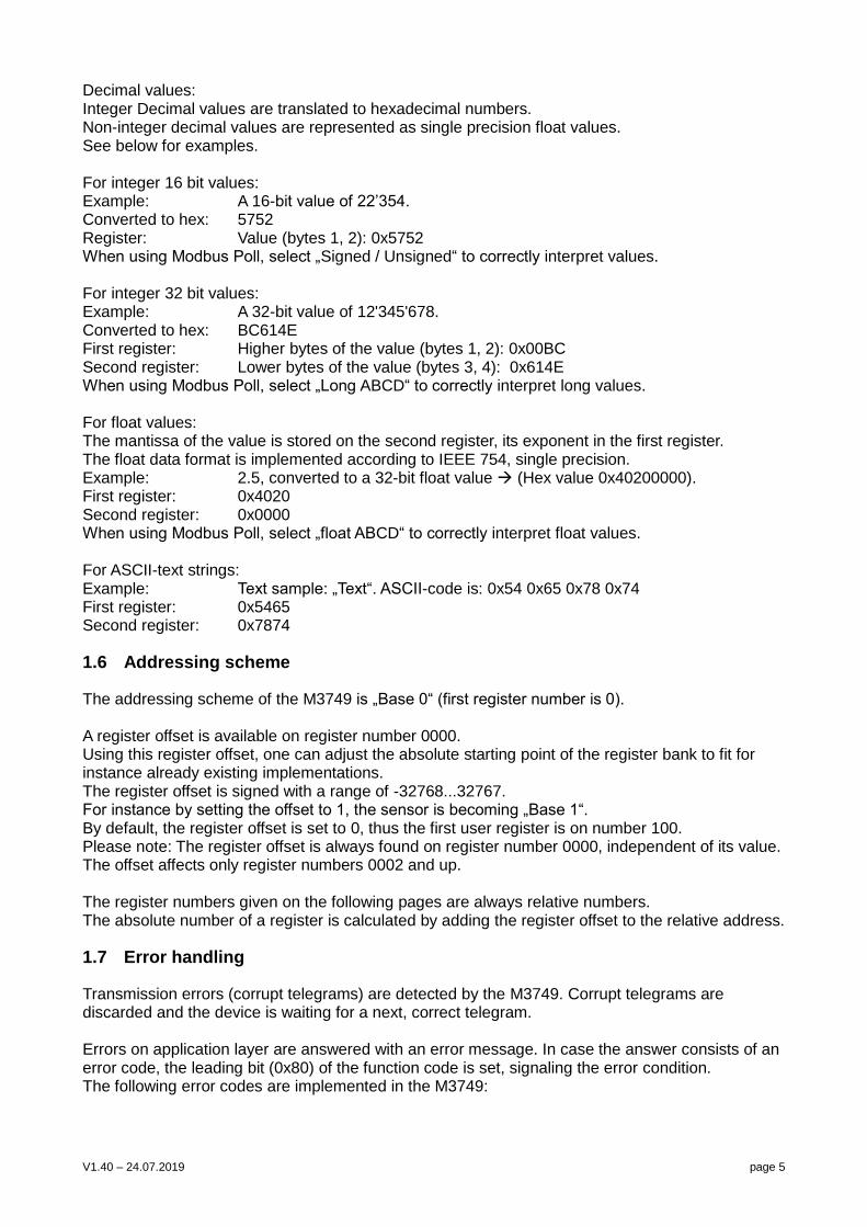
Decimal values: Integer Decimal values are translated to hexadecimal numbers. Non-integer decimal values are represented as single precision float values. See below for examples. For integer 16 bit values: Example: A 16-bit value of 22’354. Converted to hex: 5752 Register: Value (bytes 1, 2): 0x5752 When using Modbus Poll, select „Signed / Unsigned“ to correctly interpret values. For integer 32 bit values: Example: A 32-bit value of 12'345'678. Converted to hex: BC614E First register: Higher bytes of the value (bytes 1, 2): 0x00BC Second register: Lower bytes of the value (bytes 3, 4): 0x614E When using Modbus Poll, select „Long ABCD“ to correctly interpret long values. For float values: The mantissa of the value is stored on the second register, its exponent in the first register. The float data format is implemented according to IEEE 754, single precision. Example: 2.5, converted to a 32-bit float value (Hex value 0x40200000). First register: 0x4020 Second register: 0x0000 When using Modbus Poll, select „float ABCD“ to correctly interpret float values. For ASCII-text strings: Example: Text sample: „Text“. ASCII-code is: 0x54 0x65 0x78 0x74 First register: 0x5465 Second register: 0x7874
1.6 Addressing scheme
The addressing scheme of the M3749 is „Base 0“ (first register number is 0). A register offset is available on register number 0000. Using this register offset, one can adjust the absolute starting point of the register bank to fit for instance already existing implementations. The register offset is signed with a range of -32768...32767. For instance by setting the offset to 1, the sensor is becoming „Base 1“. By default, the register offset is set to 0, thus the first user register is on number 100. Please note: The register offset is always found on register number 0000, independent of its value. The offset affects only register numbers 0002 and up. The register numbers given on the following pages are always relative numbers. The absolute number of a register is calculated by adding the register offset to the relative address.
1.7 Error handling
Transmission errors (corrupt telegrams) are detected by the M3749. Corrupt telegrams are discarded and the device is waiting for a next, correct telegram. Errors on application layer are answered with an error message. In case the answer consists of an error code, the leading bit (0x80) of the function code is set, signaling the error condition. The following error codes are implemented in the M3749:

V1.40 – 24.07.2019 page 6
Error code, hex Error type
0x00 No error
0x01 Illegal function code was sent to the sensor
0x02 Illegal data address (invalid register number, access denied)
0x03 Illegal data value (value out of range)
0x04 Slave device error (operation not successfully completed)
Error code 0x01 is returned when a function code other than #3, #4, #6, #16 is sent to the M3749. Error code 0x02 is returned in the following cases:
Any attempts to undefined registers
Any attempts to registers on a higher operator level than actually selected (access denied)
When reading too many registers, so undefined registers would be attempted
When writing too many or not enough registers at once, or on a wrong starting address Error code 0x03 is returned when writing invalid data to a register. Invalid data means any value out of the range of the specific register (value below or above limits, value not part of a list of possible values). In this case, the last valid data is restored on the specific Modbus register and no change is active. Error code 0x04 is typically returned when trying to log-in to a higher user level with a wrong password or to an inexistent user level. In these cases, the log-in fail, the operation is not successfully completed.
1.8 User levels, Password protection
M3749 have implemented three user levels, level 0, 1 and 2. Reading registers is possible on any user level, except some specific registers. To prevent any unwanted configuration changes, most writing attempts are possible only on user level 2. For all user levels, default passwords are stored in the M3749. These passwords can be changed by the user. Changed passwords are stored in the non-volatile memory of the device. User levels and default passwords of the M3749:
User level Code, hex Default password, hex
0 0x03 0x00000000
1 0x0C 0x01145DEA
2 0x30 0x00F479CE
After each power-up, the device is reset to user level 0. When trying to change the user level to an invalid level or using a wrong password, the M3749 remains on the last valid user level, error code 0x04 is returned.
V1.40 – 24.07.2019 page 7
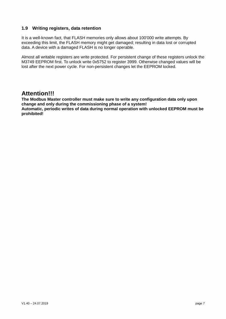
1.9 Writing registers, data retention
It is a well-known fact, that FLASH memories only allows about 100'000 write attempts. By exceeding this limit, the FLASH memory might get damaged; resulting in data lost or corrupted data. A device with a damaged FLASH is no longer operable. Almost all writable registers are write protected. For persistent change of these registers unlock the M3749 EEPROM first. To unlock write 0x5752 to register 3999. Otherwise changed values will be lost after the next power cycle. For non-persistent changes let the EEPROM locked.
Attention!!!
The Modbus Master controller must make sure to write any configuration data only upon change and only during the commissioning phase of a system! Automatic, periodic writes of data during normal operation with unlocked EEPROM must be prohibited!
V1.40 – 24.07.2019 page 8
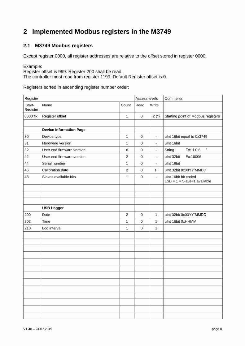
2 Implemented Modbus registers in the M3749
2.1 M3749 Modbus registers
Except register 0000, all register addresses are relative to the offset stored in register 0000. Example: Register offset is 999. Register 200 shall be read. The controller must read from register 1199. Default Register offset is 0. Registers sorted in ascending register number order:
Register Access levels Comments
Start-Register
Name Count Read Write
0000 fix Register offset 1 0 2 (*) Starting point of Modbus registers
Device Information Page
30 Device type 1 0 - uInt 16bit equal to 0x3749
31 Hardware version 1 0 - uInt 16bit
32 User end firmware version 8 0 - String Ex:“1.0.6 “
42 User end firmware version 2 0 - uInt 32bit Ex:10006
44 Serial number 1 0 - uInt 16bit
46 Calibration date 2 0 F uInt 32bit 0x00YY’MMDD
48 Slaves available bits 1 0 - uInt 16bit bit coded LSB = 1 = Slave#1 available
USB Logger
200 Date 2 0 1 uInt 32bit 0x00YY’MMDD
202 Time 1 0 1 uInt 16bit 0xHHMM
210 Log interval 1 0 1

V1.40 – 24.07.2019 page 9
Register Access levels Comments
Start-Register
Name Count Read Write
Alarm Setting Page
Alarm settings K1:
300 Cell voltage lower limit 1 0 1 uInt16bit [10mV]
301 Cell voltage upper limit 1 0 1 uInt16bit [10mV]
302 Battery current lower limit 1 0 1 Int16bit [0.1A]
303 Battery current upper limit 1 0 1 Int16bit [0.1A]
304 Temperature lower limit 1 0 1 Int16bit [0.1°C]
305 Temperature upper limit 1 0 1 Int16bit [0.1°C]
306 Auxiliary input lower limit 1 0 1 uInt16bit [0.01mA]
307 Auxiliary input upper limit 1 0 1 uInt16bit [0.01mA]
308 1 0 1
309 Cell Uripple upper limit 1 0 1 uInt16bit [10mV]
310 1 0 1
311 Cell Iripple upper limit 1 0 1 uInt16bit [0.1A]
312 1 0 1
313 Cell impedance upper limit 1 0 1 uInt16bit [0.1mΩ]
314 Battery voltage lower limit 1 0 1 uInt16bit [0.1V]
315 Battery voltage upper limit 1 0 1 uInt16bit [0.1V]
316 spare 4 0 1
320 Alarm settings K2 20 0 1 Same data structure as alarm set 1 from Reg 300-319
340 Alarm settings K3 20 0 1 Same data structure as alarm set 1 from Reg 300-319
360 Alarm K1 enable bits 1 0 1 bUcell:1 (LSB) bIbat:1 bPT100:1 bAuxInput:1 bUrippel:1 bIrippel:1 bImpedance:1 bUbat:1 reserved:8
361 Alarm K2 enable bits 1 0 1
362 Alarm K3 enable bits 1 0 1
363 Alarm K1 active 1 0 -
364 Alarm K2 active 1 0 -
365 Alarm K3 active 1 0 -
366 Relay Status 1 0 - bK1:1 (LSB) bK2:1 bK3:1 reserved:13
367 Alarm K1 upper/lower indicator 1 0 1 If corresponding active-alarm-bit is set, this reg indicates a upper limit (1) or lower limit (0) at the given alarm bit position. Same bit coding as Reg 363-365.
368 Alarm K2 upper/lower indicator 1 0 1
369 Alarm K3 upper/lower indicator 1 0 1
370 Relay K1 setting 1 0 1 bRelInverse:1 (LSB) bLedInverse:1 reserved:14 371 Relay K2 setting 1 0 1
372 Relay K3 setting 1 0 1
373 Turn on delay K1 1 0 1 uInt16 [s]
374 Turn on delay K2 1 0 1 uInt16 [s]
375 Turn on delay K3 1 0 1 uInt16 [s]
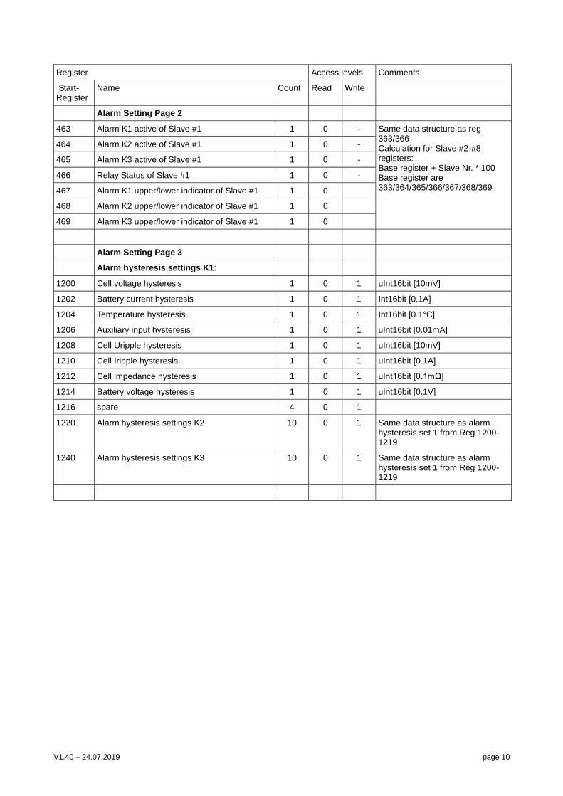
V1.40 – 24.07.2019 page 10
Register Access levels Comments
Start-Register
Name Count Read Write
Alarm Setting Page 2
463 Alarm K1 active of Slave #1 1 0 - Same data structure as reg 363/366 Calculation for Slave #2-#8 registers: Base register + Slave Nr. * 100 Base register are 363/364/365/366/367/368/369
464 Alarm K2 active of Slave #1 1 0 -
465 Alarm K3 active of Slave #1 1 0 -
466 Relay Status of Slave #1 1 0 -
467 Alarm K1 upper/lower indicator of Slave #1 1 0
468 Alarm K2 upper/lower indicator of Slave #1 1 0
469 Alarm K3 upper/lower indicator of Slave #1 1 0
Alarm Setting Page 3
Alarm hysteresis settings K1:
1200 Cell voltage hysteresis 1 0 1 uInt16bit [10mV]
1202 Battery current hysteresis 1 0 1 Int16bit [0.1A]
1204 Temperature hysteresis 1 0 1 Int16bit [0.1°C]
1206 Auxiliary input hysteresis 1 0 1 uInt16bit [0.01mA]
1208 Cell Uripple hysteresis 1 0 1 uInt16bit [10mV]
1210 Cell Iripple hysteresis 1 0 1 uInt16bit [0.1A]
1212 Cell impedance hysteresis 1 0 1 uInt16bit [0.1mΩ]
1214 Battery voltage hysteresis 1 0 1 uInt16bit [0.1V]
1216 spare 4 0 1
1220 Alarm hysteresis settings K2 10 0 1 Same data structure as alarm hysteresis set 1 from Reg 1200-1219
1240 Alarm hysteresis settings K3 10 0 1 Same data structure as alarm hysteresis set 1 from Reg 1200-1219
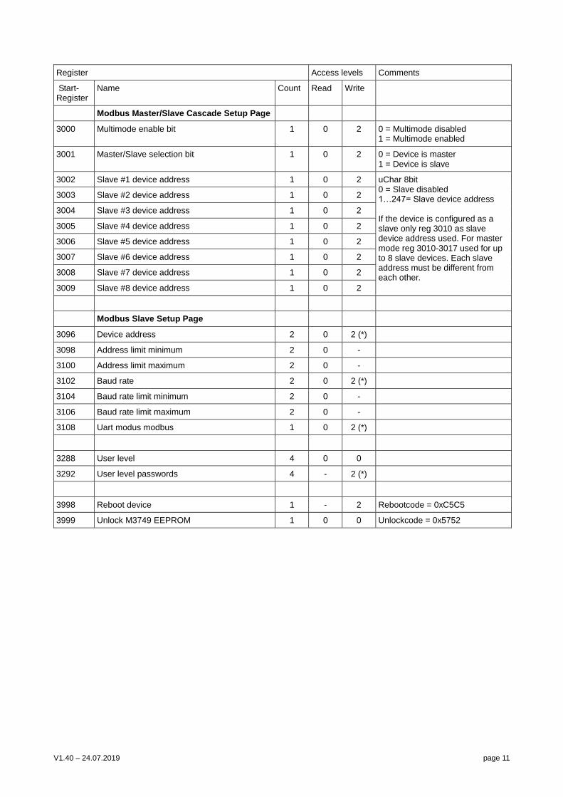
V1.40 – 24.07.2019 page 11
Register Access levels Comments
Start-Register
Name Count Read Write
Modbus Master/Slave Cascade Setup Page
3000 Multimode enable bit 1 0 2 0 = Multimode disabled 1 = Multimode enabled
3001 Master/Slave selection bit 1 0 2 0 = Device is master 1 = Device is slave
3002 Slave #1 device address 1 0 2 uChar 8bit 0 = Slave disabled 1…247= Slave device address If the device is configured as a slave only reg 3010 as slave device address used. For master mode reg 3010-3017 used for up to 8 slave devices. Each slave address must be different from each other.
3003 Slave #2 device address 1 0 2
3004 Slave #3 device address 1 0 2
3005 Slave #4 device address 1 0 2
3006 Slave #5 device address 1 0 2
3007 Slave #6 device address 1 0 2
3008 Slave #7 device address 1 0 2
3009 Slave #8 device address 1 0 2
Modbus Slave Setup Page
3096 Device address 2 0 2 (*)
3098 Address limit minimum 2 0 -
3100 Address limit maximum 2 0 -
3102 Baud rate 2 0 2 (*)
3104 Baud rate limit minimum 2 0 -
3106 Baud rate limit maximum 2 0 -
3108 Uart modus modbus 1 0 2 (*)
3288 User level 4 0 0
3292 User level passwords 4 - 2 (*)
3998 Reboot device 1 - 2 Rebootcode = 0xC5C5
3999 Unlock M3749 EEPROM 1 0 0 Unlockcode = 0x5752

V1.40 – 24.07.2019 page 12
Register Access levels Comments
Start-Register
Name Count Read Write
Statistic Control Page
4000 Clear statistic of battery & cell monitoring 1 - 1 uChar8 1= Reset
4002 Date since last reset 2 0 - uInt 32bit 0x00YY’MMDD***
4004 Time since last reset 1 0 - uInt 16bit 0xHHMM***
Battery Monitoring Page
4100 Battery I 2 0 - Float 32bit
4102 Battery I avg 2 0 - Float 32bit
4104 Battery I min 2 0 - Float 32bit
4106 Battery I max 2 0 - Float 32bit
4108 Battery Iripple 2 0 - Float 32bit
4110 Battery Irippleavg 2 0 - Float 32bit
4112 Battery Iripplemin 2 0 - Float 32bit
4114 Battery Iripplemax 2 0 - Float 32bit
4116 Temperature 2 0 - Float 32bit
4118 Temperatureavg 2 0 - Float 32bit
4120 Temperaturemin 2 0 - Float 32bit
4122 Temperaturemax 2 0 - Float 32bit
4124 Auxiliary input Aux 2 0 - Float 32bit
4126 Auxiliary input Auxavg 2 0 - Float 32bit
4128 Auxiliary input Auxmin 2 0 - Float 32bit
4130 Auxiliary input Auxmax 2 0 - Float 32bit
4132 Battery I of Slave #1 2 0 - Float 32bit Calculation for Slave #2-#8 registers: Base register + Slave Nr. * 32 Base register are 4100/4108/4116/4124
4140 Battery Iripple of Slave #1 2 0
4148 Temperatur of Slave #1 2 0
4156 Auxiliary input Aux of Slave #1 2 0
Battery Monitoring Page 2
4390 Number of connected cells 1 0 uInt 16bit
4392 Battery voltage 2 0 Float 32bit
4394 Cell average voltage 2 0 Float 32bit
4396 Cell connected summary 4 0 uInt 64bit Bit coded cell connected flag
4400 Battery impedance 2 0 Float 32bit
4402 Battery Monitoring Page 2 of Slave #1 - #8 96 0 Same data structure as reg 4390-4400
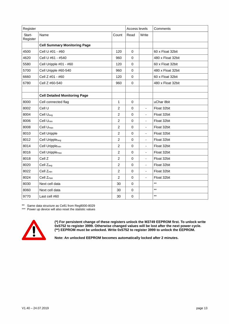
V1.40 – 24.07.2019 page 13
Register Access levels Comments
Start-Register
Name Count Read Write
Cell Summary Monitoring Page
4500 Cell U #01 - #60 120 0 60 x Float 32bit
4620 Cell U #61 - #540 960 0 480 x Float 32bit
5580 Cell Uripple #01 - #60 120 0 60 x Float 32bit
5700 Cell Uripple #60-540 960 0 480 x Float 32bit
6660 Cell Z #01 - #60 120 0 60 x Float 32bit
6780 Cell Z #60-540 960 0 480 x Float 32bit
Cell Detailed Monitoring Page
8000 Cell connected flag 1 0 uChar 8bit
8002 Cell U 2 0 - Float 32bit
8004 Cell Uavg 2 0 - Float 32bit
8006 Cell Umin 2 0 - Float 32bit
8008 Cell Umax 2 0 - Float 32bit
8010 Cell Uripple 2 0 - Float 32bit
8012 Cell Urippleavg 2 0 - Float 32bit
8014 Cell Uripplemin 2 0 - Float 32bit
8016 Cell Uripplemax 2 0 - Float 32bit
8018 Cell Z 2 0 - Float 32bit
8020 Cell Zavg 2 0 - Float 32bit
8022 Cell Zmin 2 0 - Float 32bit
8024 Cell Zmax 2 0 - Float 32bit
8030 Next cell data 30 0 **
8060 Next cell data 30 0 **
9770 Last cell #60 30 0 **
** Same data structure as Cell1 from Reg8000-8029 *** Power up device will also reset the statistic values
(*) For persistent change of these registers unlock the M3749 EEPROM first. To unlock write 0x5752 to register 3999. Otherwise changed values will be lost after the next power cycle. (**) EEPROM must be unlocked. Write 0x5752 to register 3999 to unlock the EEPROM.
Note: An unlocked EEPROM becomes automatically locked after 2 minutes.
V1.40 – 24.07.2019 page 14
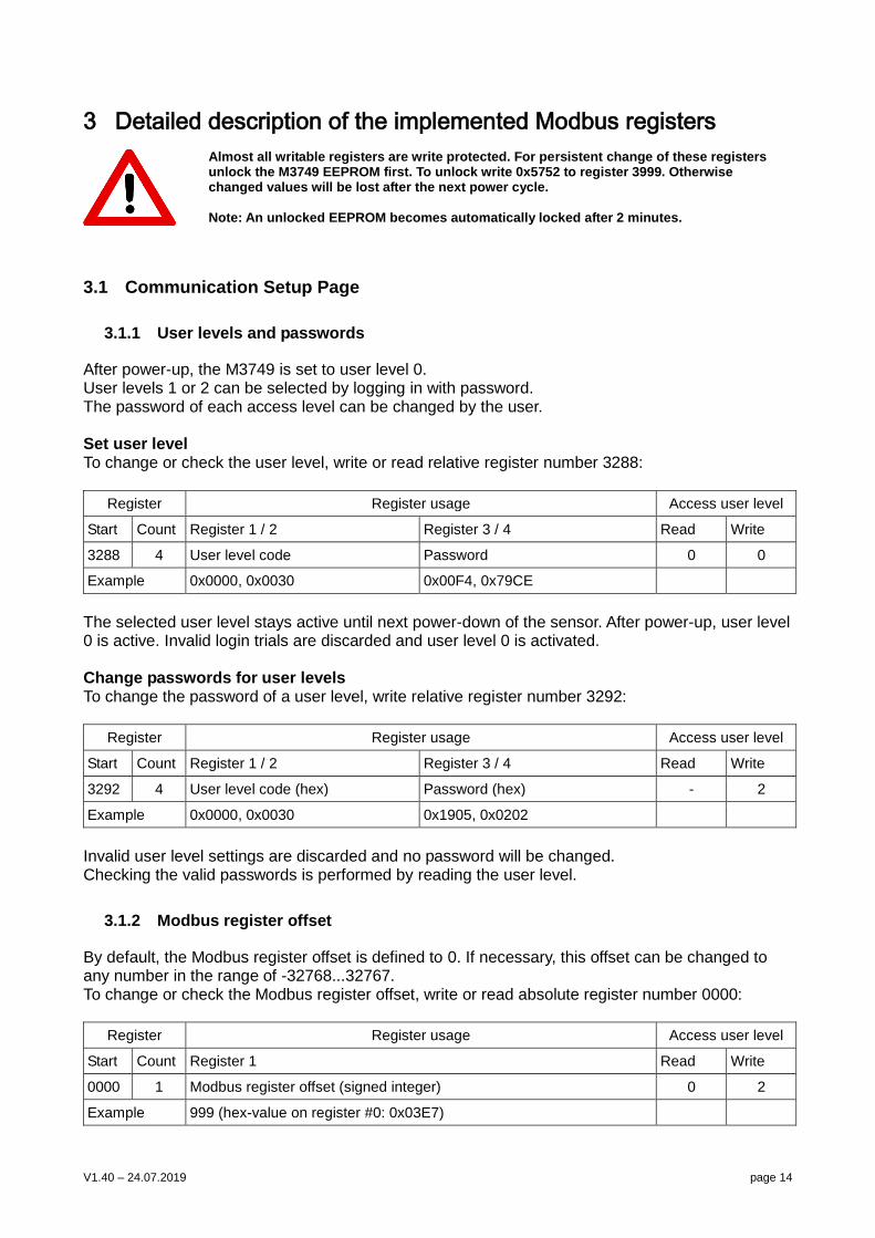
3 Detailed description of the implemented Modbus registers
Almost all writable registers are write protected. For persistent change of these registers unlock the M3749 EEPROM first. To unlock write 0x5752 to register 3999. Otherwise changed values will be lost after the next power cycle.
Note: An unlocked EEPROM becomes automatically locked after 2 minutes.
3.1 Communication Setup Page
3.1.1 User levels and passwords
After power-up, the M3749 is set to user level 0. User levels 1 or 2 can be selected by logging in with password. The password of each access level can be changed by the user. Set user level To change or check the user level, write or read relative register number 3288:
Register Register usage Access user level
Start Count Register 1 / 2 Register 3 / 4 Read Write
3288 4 User level code Password 0 0
Example 0x0000, 0x0030 0x00F4, 0x79CE
The selected user level stays active until next power-down of the sensor. After power-up, user level 0 is active. Invalid login trials are discarded and user level 0 is activated. Change passwords for user levels To change the password of a user level, write relative register number 3292:
Register Register usage Access user level
Start Count Register 1 / 2 Register 3 / 4 Read Write
3292 4 User level code (hex) Password (hex) - 2
Example 0x0000, 0x0030 0x1905, 0x0202
Invalid user level settings are discarded and no password will be changed. Checking the valid passwords is performed by reading the user level.
3.1.2 Modbus register offset
By default, the Modbus register offset is defined to 0. If necessary, this offset can be changed to any number in the range of -32768...32767. To change or check the Modbus register offset, write or read absolute register number 0000:
Register Register usage Access user level
Start Count Register 1 Read Write
0000 1 Modbus register offset (signed integer) 0 2
Example 999 (hex-value on register #0: 0x03E7)
V1.40 – 24.07.2019 page 15
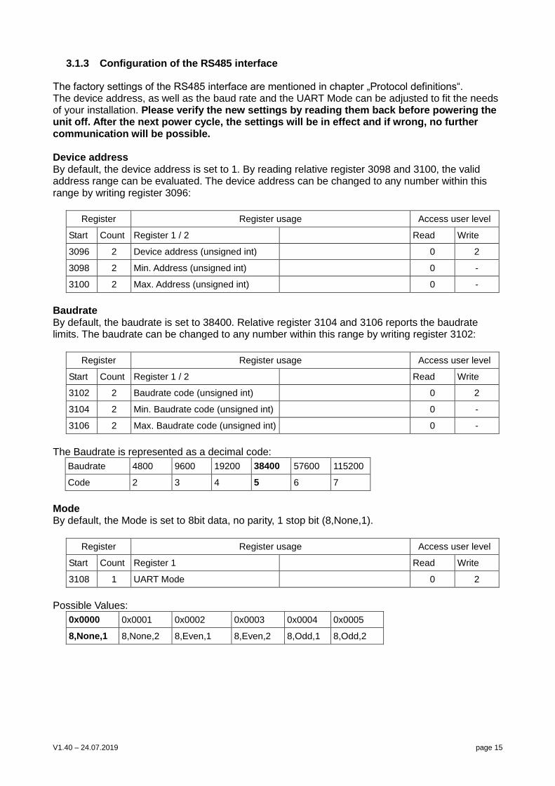
3.1.3 Configuration of the RS485 interface
The factory settings of the RS485 interface are mentioned in chapter „Protocol definitions“. The device address, as well as the baud rate and the UART Mode can be adjusted to fit the needs of your installation. Please verify the new settings by reading them back before powering the unit off. After the next power cycle, the settings will be in effect and if wrong, no further communication will be possible. Device address By default, the device address is set to 1. By reading relative register 3098 and 3100, the valid address range can be evaluated. The device address can be changed to any number within this range by writing register 3096:
Register Register usage Access user level
Start Count Register 1 / 2 Read Write
3096 2 Device address (unsigned int) 0 2
3098 2 Min. Address (unsigned int) 0 -
3100 2 Max. Address (unsigned int) 0 -
Baudrate By default, the baudrate is set to 38400. Relative register 3104 and 3106 reports the baudrate limits. The baudrate can be changed to any number within this range by writing register 3102:
Register Register usage Access user level
Start Count Register 1 / 2 Read Write
3102 2 Baudrate code (unsigned int) 0 2
3104 2 Min. Baudrate code (unsigned int) 0 -
3106 2 Max. Baudrate code (unsigned int) 0 -
The Baudrate is represented as a decimal code:
Baudrate 4800 9600 19200 38400 57600 115200
Code 2 3 4 5 6 7
Mode By default, the Mode is set to 8bit data, no parity, 1 stop bit (8,None,1).
Register Register usage Access user level
Start Count Register 1 Read Write
3108 1 UART Mode 0 2
Possible Values:
0x0000 0x0001 0x0002 0x0003 0x0004 0x0005
8,None,1 8,None,2 8,Even,1 8,Even,2 8,Odd,1 8,Odd,2