document number: mmg15241h technical data rev. 2, 9/2014 … · enhancement mode phemt technology...
TRANSCRIPT
MMG15241HT1
1RF Device DataFreescale Semiconductor, Inc.
Enhancement Mode pHEMTTechnology (E--pHEMT)High Linearity AmplifierThe MMG15241H is a high dynamic range, low noise amplifier MMIC, housed
in a SOT--89 standard plastic package. It is ideal for cellular, PCS, LTE,TD--SCDMA, W--CDMA base station, wireless LAN and other systems in the500 to 2800 MHz frequency range. With high OIP3 and low noise figure, it canbe utilized as a driver amplifier in the transmit chain and as a second stage LNAin the receive chain.Features
Frequency: 500--2800 MHz Noise Figure: 1.6 dB @ 2140 MHz P1dB: 24 dBm @ 2140 MHz Small--Signal Gain: 15.9 dB @ 2140 MHz Third Order Output Intercept Point: 39.4 dBm @ 2140 MHz Single 5 V Supply Supply Current: 85 mA 50 Ohm Operation (some external matching required) Cost--effective SOT--89 Surface Mount Plastic Package In Tape and Reel. T1 Suffix = 1,000 Units, 12 mm Tape Width, 7--inch Reel.
Table 1. Typical Performance (1)
Characteristic Symbol900MHz
2140MHz
2600MHz Unit
Noise Figure NF 1.2 1.6 1.3 dB
Input Return Loss(S11)
IRL --11.8 --21.3 --16.9 dB
Output Return Loss(S22)
ORL --13.4 --16.2 --20.9 dB
Small--Signal Gain(S21)
Gp 20.5 15.9 14.4 dB
Power Output @ 1dBCompression
P1db 24 24 24 dBm
Third Order InputIntercept Point
IIP3 18.2 23.5 26.2 dBm
Third Order OutputIntercept Point
OIP3 38.7 39.4 40.6 dBm
1. VDD = 5 Vdc, TA = 25C, 50 ohm system, application circuittuned for specified frequency.
Table 2. Maximum Ratings
Rating Symbol Value Unit
Supply Voltage VDD 6 V
Supply Current IDD 130 mA
RF Input Power Pin 23 dBm
Storage Temperature Range Tstg --65 to +150 C
Junction Temperature TJ 175 C
Table 3. Thermal Characteristics
Characteristic Symbol Value (2) Unit
Thermal Resistance, Junction to CaseCase Temperature 85C, 5 Vdc, 84 mA, no RF applied
RJC 59 C/W
2. Refer to AN1955, Thermal Measurement Methodology of RF Power Amplifiers. Go to http://www.freescale.com/rf.Select Documentation/Application Notes -- AN1955.
Freescale SemiconductorTechnical Data
Document Number: MMG15241HRev. 2, 9/2014
MMG15241HT1
500--2800 MHz, 15.9 dB24 dBm
E--pHEMT LNA/GPA
SOT--89
Freescale Semiconductor, Inc., 2010–2011, 2014. All rights reserved.

2RF Device Data
Freescale Semiconductor, Inc.
MMG15241HT1
Table 4. Electrical Characteristics (VDD = 5 Vdc, 2140 MHz, TA = 25C, 50 ohm system, in Freescale Application Circuit)
Characteristic Symbol Min Typ Max Unit
Small--Signal Gain (S21) Gp 14 15.9 — dB
Input Return Loss (S11) IRL — --21.3 — dB
Output Return Loss (S22) ORL — --16.2 — dB
Power Output @ 1dB Compression P1dB — 24 — dBm
Third Order Input Intercept Point IIP3 — 23.5 — dBm
Third Order Output Intercept Point OIP3 — 39.4 — dBm
Reverse Isolation (S12) |S12| — --22.5 — dB
Noise Figure NF — 1.6 — dB
Supply Current IDD 65 85 105 mA
Supply Voltage VDD — 5 — V
Table 5. Functional Pin Description
PinNumber Pin Function
1 RFin
2 Ground
3 RFout/DC Supply
Table 6. ESD Protection Characteristics
Test Methodology Class
Human Body Model (per JESD 22--A114) 1A
Machine Model (per EIA/JESD 22--A115) A
Charge Device Model (per JESD 22--C101) IV
Table 7. Moisture Sensitivity Level
Test Methodology Rating Package Peak Temperature Unit
Per JESD22--A113, IPC/JEDEC J--STD--020 1 260 C
Figure 1. Functional Diagram
321
2

MMG15241HT1
3RF Device DataFreescale Semiconductor, Inc.
50 OHM TYPICAL CHARACTERISTICS
0 1 1.5 2.5 30.5 29
25
0
TC = 25C
f, FREQUENCY (GHz)
Figure 2. Small--Signal Gain (S21) versusFrequency (1)
21
13
1 1.5 2.5 3
Gp,SM
ALL--SIGNAL
GAIN(dB)
85C
--40C
--30
10
S22
f, FREQUENCY (GHz)
Figure 3. Input/Output Return Loss versusFrequency (1)
VDD = 5 Vdc
S110
--10
--20
S11,S22(dB)
VDD = 5 Vdc
17
0.5 2
1. Test fixture characteristics have been mathematically removed from the graphical data.

4RF Device Data
Freescale Semiconductor, Inc.
MMG15241HT1
50 OHM APPLICATION CIRCUIT: 2140 MHz
Figure 4. MMG15241HT1 Test Circuit Schematic
RFOUTPUT
RFINPUT
VSUPPLY
C4
C6
Z1 Z2
C2
Z6 Z7
C3
L1
Z3DUT
Z1 0.026 x 0.021 MicrostripZ2 0.168 x 0.021 MicrostripZ3 0.030 x 0.044 MicrostripZ4 0.200 x 0.042 Microstrip
Z5 0.030 x 0.044 MicrostripZ6 0.172 x 0.021 MicrostripZ7 0.353 x 0.021 Microstrip
Z5
C1
Z4
C5
Table 8. MMG15241HT1 Test Circuit Component Designations and ValuesPart Description Part Number Manufacturer
C1 1.5 pF Chip Capacitor GJM1555C1H1R5CB01D Murata
C2 0.8 pF Chip Capacitor GJM1555C1HR80BB01D Murata
C3 0.7 pF Chip Capacitor GJM1555C1HR70BB01D Murata
C4 56 pF Chip Capacitor GRM188RC1H560GA01D Murata
C5 0.1 F Chip Capacitor GRM188R71H104KA93D Murata
C6 5.6 pF Chip Capacitor GJM1555C1H5R6DB01D Murata
L1 30 nH Chip Inductor 0603CS--30NXJLW Coilcraft
PCB 0.010, r = 3.38, Multilayer IS680--338 Isola

MMG15241HT1
5RF Device DataFreescale Semiconductor, Inc.
50 OHM APPLICATION CIRCUIT: 2140 MHz
Figure 5. MMG15241HT1 Test Circuit Component Layout
SOT--89--3BRev. 0
C1
RFIN RFOUT
C2
C6
C3
L1
C4
C5
VDD
Table 8. MMG15241HT1 Test Circuit Component Designations and ValuesPart Description Part Number Manufacturer
C1 1.5 pF Chip Capacitor GJM1555C1H1R5CB01D Murata
C2 0.8 pF Chip Capacitor GJM1555C1HR80BB01D Murata
C3 0.7 pF Chip Capacitor GJM1555C1HR70BB01D Murata
C4 56 pF Chip Capacitor GRM188RC1H560GA01D Murata
C5 0.1 F Chip Capacitor GRM188R71H104KA93D Murata
C6 5.6 pF Chip Capacitor GJM1555C1H5R6DB01D Murata
L1 30 nH Chip Inductor 0603CS--30NXJLW Coilcraft
PCB 0.010, r = 3.38, Multilayer IS680--338 Isola
(Component Designations and Values table repeated for reference.)
6RF Device Data
Freescale Semiconductor, Inc.
MMG15241HT1
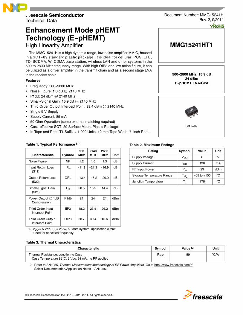
50 OHM TYPICAL CHARACTERISTICS: 2140 MHz
37
41
39
2040 2090 2140 2190 2240
40
38
VDD = 5 Vdc
TC = 25C
--40C
85C
13
17
2000
f, FREQUENCY (MHz)
Figure 6. Small--Signal Gain (S21) versusFrequency
VDD = 5 Vdc
15
Gp,SM
ALL--SIGNAL
GAIN(dB)
16
14
2075 2150 2225 2300
TC = --40C
85C25C
--24
--8
f, FREQUENCY (MHz)
Figure 7. Input Return Loss (S11) versusFrequency
IRL,INPUTRETURNLOSS
(dB)
--16
VDD = 5 Vdc
2000 2075 2150 2225 2300
--12
--20
TC = --40C
85C
25C
--25
--5
f, FREQUENCY (MHz)
Figure 8. Output Return Loss (S22) versusFrequency
ORL,OUTPUTRETURNLOSS
(dB)
--15
VDD = 5 Vdc
2000 2075 2150 2225 2300
--10
--20
25C
21
25
23
22
f, FREQUENCY (MHz)
Figure 9. P1dB versus Frequency
P1dB,1dB
COMPRESSIONPOINT(dBm
)
24
VDD = 5 Vdc
TC = --40C
25C85C
2040 2090 2140 2190 2240
f, FREQUENCY (MHz)
Figure 10. Third Order Output InterceptPoint versus Frequency
OIP3,THIRDORDER
OUTPUTINTERCEPTPOINT(dBm
)
0.8
2.4
f, FREQUENCY (MHz)
Figure 11. Noise Figure versus Frequency
1.6
1.2NF,NOISEFIGURE(dB)
VDD = 5 Vdc
TC = 85C
25C
--40C
2
2000 2075 2150 2225 2300
TC = --40C
85C
MMG15241HT1
7RF Device DataFreescale Semiconductor, Inc.
50 OHM TYPICAL CHARACTERISTICS: 2140 MHz
--55
--15
14
Pout, OUTPUT POWER (dBm)
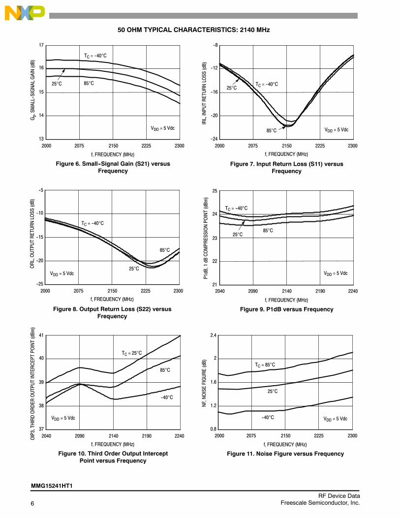
Figure 12. Single--Carrier W--CDMA AdjacentChannel Power Ratio versus Output Power
--25
--35
--45
2421.51916.5
ACPR,ADJACENTCHANNEL
POWER
RATIO(dBc)
TC = 85C25C
--40C
VDD = 5 Vdc, f = 2140 MHz, Single--Carrier W--CDMA3.84 MHz Channel Bandwidth, Input SignalPAR = 8.5 dB @ 0.01% Probability (CCDF)

8RF Device Data
Freescale Semiconductor, Inc.
MMG15241HT1
50 OHM APPLICATION CIRCUIT: 900 MHz
Figure 13. MMG15241HT1 Test Circuit Schematic
RFOUTPUT
RFINPUT
VSUPPLY
C3 C4
C5
Z1
C1 C2
R1
L1
Z3Z2DUT
Z1 0.041 x 0.058 MicrostripZ2 0.112 x 0.058 Microstrip
Z3 0.090 x 0.058 MicrostripZ4 0.085 x 0.058 Microstrip
Z4
L2
Table 9. MMG15241HT1 Test Circuit Component Designations and ValuesPart Description Part Number Manufacturer
C1 3.9 pF Chip Capacitor GQM1885C2A3R9CB01 Murata
C2 0.6 pF Chip Capacitor GQM1885C2AR60CB01 Murata
C3, C5 56 pF Chip Capacitors GRM188RC1H560GA01D Murata
C4 0.1 F Chip Capacitor GRM188R71H104KA93D Murata
L1 30 nH Chip Inductor 0603CS--30NXJLW Coilcraft
L2 6.8 nH Chip Inductor 0603CS--6N8XJLW Coilcraft
R1 0 Ω, 1 A Chip Resistor ERJ3GEY0R00V Panasonic
PCB 0.031, r = 4.1 Getek Grade ML200C GE Electromaterials
Figure 14. MMG15241HT1 Test Circuit Component Layout
C1
L1 C5
R1
C4
C3
SOT--89--3A
Rev. 0
L2
C2

MMG15241HT1
9RF Device DataFreescale Semiconductor, Inc.
50 OHM TYPICAL CHARACTERISTICS: 900 MHz
36
40
38
39
37
VDD = 5 Vdc
18
22
750
f, FREQUENCY (MHz)
Figure 15. Small--Signal Gain (S21) versusFrequency
VDD = 5 Vdc
20
Gp,SM
ALL--SIGNAL
GAIN(dB)
21
19
825 900 975 1050--15
--3
f, FREQUENCY (MHz)
Figure 16. Input Return Loss (S11) versusFrequency
IRL,INPUTRETURNLOSS
(dB)
--9
VDD = 5 Vdc
--6
--12
--24
--8
f, FREQUENCY (MHz)
Figure 17. Output Return Loss (S22) versusFrequency
ORL,OUTPUTRETURNLOSS
(dB)
--16
VDD = 5 Vdc
--12
--20
22
26
24
23
f, FREQUENCY (MHz)
Figure 18. P1dB versus Frequency
P1dB,1dB
COMPRESSIONPOINT(dBm
)25
VDD = 5 Vdc
800 850 900 950 1000
f, FREQUENCY (MHz)
Figure 19. Third Order Output InterceptPoint versus Frequency
OIP3,THIRDORDER
OUTPUTINTERCEPTPOINT(dBm
)
0
2
f, FREQUENCY (MHz)
Figure 20. Noise Figure versus Frequency
1
0.5NF,NOISEFIGURE(dB)
VDD = 5 Vdc
1.5
750 825 900 975 1050
750 825 900 975 1050
800 850 900 950 1000 750 825 900 975 1050

10RF Device Data
Freescale Semiconductor, Inc.
MMG15241HT1
50 OHM APPLICATION CIRCUIT: 2600 MHz
Figure 21. MMG15241HT1 Test Circuit Schematic
RFOUTPUT
RFINPUT
VSUPPLY
C4
C6
Z1 Z5 Z6
C3
L1
Z2DUT
Z1 0.149 x 0.021 MicrostripZ2 0.030 x 0.044 MicrostripZ3 0.200 x 0.042 MicrostripZ4 0.030 x 0.044 Microstrip
Z5 0.166 x 0.021 MicrostripZ6 0.088 x 0.021 MicrostripZ7 0.215 x 0.021 Microstrip
Z4
C1
Z3
C5
C2
Z7
Table 10. MMG15241HT1 Test Circuit Component Designations and ValuesPart Description Part Number Manufacturer
C1 1.0 pF Chip Capacitor GJM1555C1H1R0CB01D Murata
C2 0.4 pF Chip Capacitor GJM1555C1HR40BB01D Murata
C3 0.2 pF Chip Capacitor GJM1555C1HR20BB01D Murata
C4 56 pF Chip Capacitor GRM188RC1H560GA01D Murata
C5 0.1 F Chip Capacitor GRM188R71H104KA93D Murata
C6 10 pF Chip Capacitor GJM1555C1H100JB01D Murata
L1 30 nH Chip Inductor 0603CS--30NXJLW Coilcraft
PCB 0.010, r = 3.38, Multilayer IS680--338 Isola

MMG15241HT1
11RF Device DataFreescale Semiconductor, Inc.
50 OHM APPLICATION CIRCUIT: 2600 MHz
Figure 22. MMG15241HT1 Test Circuit Component Layout
SOT--89--3BRev. 0
C1
RFIN RFOUT
VDD
C6C2
C3
L1
C4
C5
Table 10. MMG15241HT1 Test Circuit Component Designations and ValuesPart Description Part Number Manufacturer
C1 1.0 pF Chip Capacitor GJM1555C1H1R0CB01D Murata
C2 0.4 pF Chip Capacitor GJM1555C1HR40BB01D Murata
C3 0.2 pF Chip Capacitor GJM1555C1HR20BB01D Murata
C4 56 pF Chip Capacitor GRM188RC1H560GA01D Murata
C5 0.1 F Chip Capacitor GRM188R71H104KA93D Murata
C6 10 pF Chip Capacitor GJM1555C1H100JB01D Murata
L1 30 nH Chip Inductor 0603CS--30NXJLW Coilcraft
PCB 0.010, r = 3.38, Multilayer IS680--338 Isola
(Component Designations and Values table repeated for reference.)

12RF Device Data
Freescale Semiconductor, Inc.
MMG15241HT1
50 OHM TYPICAL CHARACTERISTICS: 2600 MHz
36
42
39
40.5
37.5
13
15
2450
f, FREQUENCY (MHz)
Figure 23. Small--Signal Gain (S21) versusFrequency
VDD = 5 Vdc
14
Gp,SM
ALL--SIGNAL
GAIN(dB)
14.5
13.5
2525 2600 2675 2750--18
--10
f, FREQUENCY (MHz)
Figure 24. Input Return Loss (S11) versusFrequency
IRL,INPUTRETURNLOSS
(dB)
--14
VDD = 5 Vdc
--12
--16
--24
--16
f, FREQUENCY (MHz)
Figure 25. Output Return Loss (S22) versusFrequency
ORL,OUTPUTRETURNLOSS
(dB)
--20
VDD = 5 Vdc
--18
--22
22
25
23.5
22.75
f, FREQUENCY (MHz)
Figure 26. P1dB versus Frequency
P1dB,1dB
COMPRESSIONPOINT(dBm
)
24.25
VDD = 5 Vdc
2500 2550 2600 2650 2700
f, FREQUENCY (MHz)
Figure 27. Third Order Output InterceptPoint versus Frequency
OIP3,THIRDORDER
OUTPUTINTERCEPTPOINT(dBm
)
1
2
f, FREQUENCY (MHz)
Figure 28. Noise Figure versus Frequency
1.5
1.25NF,NOISEFIGURE(dB)
VDD = 5 Vdc
1.75
2450 2525 2600 2675 2750
2450 2525 2600 2675 2750
2500 2550 2600 2650 2700 2450 2525 2600 2675 2750
VDD = 5 Vdc
MMG15241HT1
13RF Device DataFreescale Semiconductor, Inc.
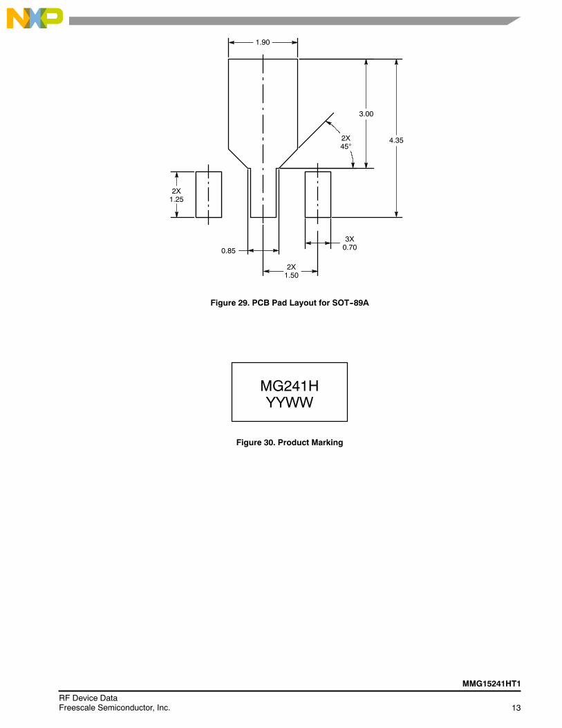
Figure 29. PCB Pad Layout for SOT--89A
4.35
3.00
2X45
3X0.70
2X1.50
0.85
2X1.25
1.90
Figure 30. Product Marking
MG241HYYWW

14RF Device Data
Freescale Semiconductor, Inc.
MMG15241HT1
PACKAGE DIMENSIONS

MMG15241HT1
15RF Device DataFreescale Semiconductor, Inc.

16RF Device Data
Freescale Semiconductor, Inc.
MMG15241HT1

MMG15241HT1
17RF Device DataFreescale Semiconductor, Inc.
PRODUCT DOCUMENTATION, TOOLS AND SOFTWARE
Refer to the following resources to aid your design process.
Application Notes
AN1955: Thermal Measurement Methodology of RF Power AmplifiersSoftware
.s2p FileDevelopment Tools
Printed Circuit Boards
For Software and Tools, do a Part Number search at http://www.freescale.com, and select the “Part Number” link. Go toSoftware & Tools on the part’s Product Summary page to download the respective tool.
FAILURE ANALYSIS
At this time, because of the physical characteristics of the part, failure analysis is limited to electrical signature analysis. Incases where Freescale is contractually obligated to perform failure analysis (FA) services, full FA may be performed by thirdparty vendors with moderate success. For updates contact your local Freescale Sales Office.
REVISION HISTORY
The following table summarizes revisions to this document.
Revision Date Description
0 Dec. 2010 Initial Release of Data Sheet
1 Apr. 2011 Table 2, Maximum Ratings, updated RF Input Power from 13 dBm to 23 dBm as a result of newmeasurements done over temperature and bias, p. 1
2 Sept. 2014 Table 2, Maximum Ratings: updated Junction Temperature from 150C to 175C to reflect recent testresults of the device, p. 1
Table 6, ESD Protection Characteristics: Changed ESD Human Body Model rating from 2 to 1A andMachine Model rating from B to A to reflect recent ESD test results of the device; removed the word“Minimum” after the ESD class rating. ESD ratings are characterized during new product development butare not 100% tested during production. ESD ratings provided in the data sheet are intended to be used asa guideline when handling ESD sensitive devices, p. 2
Revised Failure Analysis information, p. 17

18RF Device Data
Freescale Semiconductor, Inc.
MMG15241HT1
Information in this document is provided solely to enable system and softwareimplementers to use Freescale products. There are no express or implied copyrightlicenses granted hereunder to design or fabricate any integrated circuits based on theinformation in this document.
Freescale reserves the right to make changes without further notice to any productsherein. Freescale makes no warranty, representation, or guarantee regarding thesuitability of its products for any particular purpose, nor does Freescale assume anyliability arising out of the application or use of any product or circuit, and specificallydisclaims any and all liability, including without limitation consequential or incidentaldamages. “Typical” parameters that may be provided in Freescale data sheets and/orspecifications can and do vary in different applications, and actual performance mayvary over time. All operating parameters, including “typicals,” must be validated foreach customer application by customer’s technical experts. Freescale does not conveyany license under its patent rights nor the rights of others. Freescale sells productspursuant to standard terms and conditions of sale, which can be found at the followingaddress: freescale.com/SalesTermsandConditions.
Freescale and the Freescale logo are trademarks of Freescale Semiconductor, Inc.,Reg. U.S. Pat. & Tm. Off. All other product or service names are the property of theirrespective owners.E 2010--2011, 2014 Freescale Semiconductor, Inc.
How to Reach Us:
Home Page:freescale.com
Web Support:freescale.com/support
Document Number: MMG15241HRev. 2, 9/2014