dn81 lighting handbooke2... · lighting handbook introduction this handbook is a convenient...
TRANSCRIPT
Issue 6 - November 2006 1 www.zetex.com© Zetex Semiconductors plc 2006
DN81
Lighting handbook
Introduction
This handbook is a convenient collection of design and application notes that have beendeveloped to support lighting application requirements. These notes demonstrate the power andflexibility of the Zetex range of lighting DC-DC converters, switches and diodes. Application fitscan be found for a wide range of end equipment, from driving white LEDs for back lighting colorLCD displays, to single cell LED flash lights.
The products used in these notes are:
• ZXSC300 Single/multi cell LED driver
• ZXSC310 Single/multi cell LED drive with shut down
• ZXSC310 with reverse polarity protection
• ZXSC300 / ZXSC310 A high power LED driver for low voltage halogen replacement
• ZXSC400 LED driver with shut down
• ZXLD1100, ZXLD1101 LED drive with integrated switch
• ZXLB1600 LCD/OLED bias generator
• FMMT617, FMMT618, FMMT619 Low saturation NPN switch
• ZHCS500, ZHCS1000, ZHCS2000 Low VF Schottky diode
• ZXLD1350 350mA LED driver with internal switch
Individual datasheets for these devices can be found on www.zetex.com
All the designs have been built and evaluated. However, users should satisfy themselves of thesuitability for their specific application.
www.zetex.com 2 Issue 6 - November 2006
© Zetex Semiconductors plc 2006
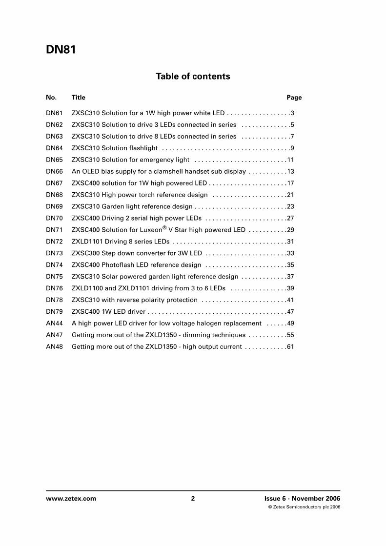
Table of contents
No. Title Page
DN61 ZXSC310 Solution for a 1W high power white LED . . . . . . . . . . . . . . . . . .3
DN62 ZXSC310 Solution to drive 3 LEDs connected in series . . . . . . . . . . . . . .5
DN63 ZXSC310 Solution to drive 8 LEDs connected in series . . . . . . . . . . . . . .7
DN64 ZXSC310 Solution flashlight . . . . . . . . . . . . . . . . . . . . . . . . . . . . . . . . . . . .9
DN65 ZXSC310 Solution for emergency light . . . . . . . . . . . . . . . . . . . . . . . . . .11
DN66 An OLED bias supply for a clamshell handset sub display . . . . . . . . . . .13
DN67 ZXSC400 solution for 1W high powered LED . . . . . . . . . . . . . . . . . . . . . .17
DN68 ZXSC310 High power torch reference design . . . . . . . . . . . . . . . . . . . . .21
DN69 ZXSC310 Garden light reference design . . . . . . . . . . . . . . . . . . . . . . . . . .23
DN70 ZXSC400 Driving 2 serial high power LEDs . . . . . . . . . . . . . . . . . . . . . . .27
DN71 ZXSC400 Solution for Luxeon® V Star high powered LED . . . . . . . . . . .29
DN72 ZXLD1101 Driving 8 series LEDs . . . . . . . . . . . . . . . . . . . . . . . . . . . . . . . .31
DN73 ZXSC300 Step down converter for 3W LED . . . . . . . . . . . . . . . . . . . . . . .33
DN74 ZXSC400 Photoflash LED reference design . . . . . . . . . . . . . . . . . . . . . . .35
DN75 ZXSC310 Solar powered garden light reference design . . . . . . . . . . . . .37
DN76 ZXLD1100 and ZXLD1101 driving from 3 to 6 LEDs . . . . . . . . . . . . . . . .39
DN78 ZXSC310 with reverse polarity protection . . . . . . . . . . . . . . . . . . . . . . . .41
DN79 ZXSC400 1W LED driver . . . . . . . . . . . . . . . . . . . . . . . . . . . . . . . . . . . . . . .47
AN44 A high power LED driver for low voltage halogen replacement . . . . . .49
AN47 Getting more out of the ZXLD1350 - dimming techniques . . . . . . . . . . .55
AN48 Getting more out of the ZXLD1350 - high output current . . . . . . . . . . . .61
DN81

DN61
ZXSC310 Solution for a 1W high power white LED
Description
This design note shows the ZXSC310 driving a 1W LED. The LED has 180Cd light output from aforward current of 350mA. The solution is optimized to drive the 1W LED at 350mA DC currentfrom a dual cell input.
Figure 1 Schematic diagram
Figure 2 Performance graphs
Issue 4 - July 2006 3 www.zetex.com© Zetex Semiconductors plc 2006

DN61
Reference Part no. Value Manufacturer Contact details
U1 ZXSC310E5 LED driver Zetex www.zetex.com
Q1 FMMT617 3A, low VCE(sat) Zetex www.zetex.com
D1 ZHCS1000 2A, low VF Zetex www.zetex.com
L1 DO3316P-223 22H, 2A Coilcraft www.coilcraft.com
R1 Generic 22m Generic NA
C1 Generic 2.2F Generic NA
LED1 LXHL-NW98 White LED Lumileds www.lumileds.com
Table 1 Bill of materials
www.zetex.com 4 Issue 4 - July 2006© Zetex Semiconductors plc 2006
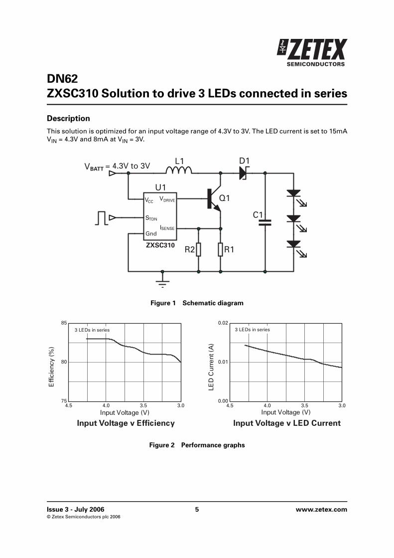
DN62
ZXSC310 Solution to drive 3 LEDs connected in series
Description
This solution is optimized for an input voltage range of 4.3V to 3V. The LED current is set to 15mAVIN = 4.3V and 8mA at VIN = 3V.
Figure 1 Schematic diagram
Figure 2 Performance graphs
ZXSC310
Issue 3 - July 2006 5 www.zetex.com© Zetex Semiconductors plc 2006
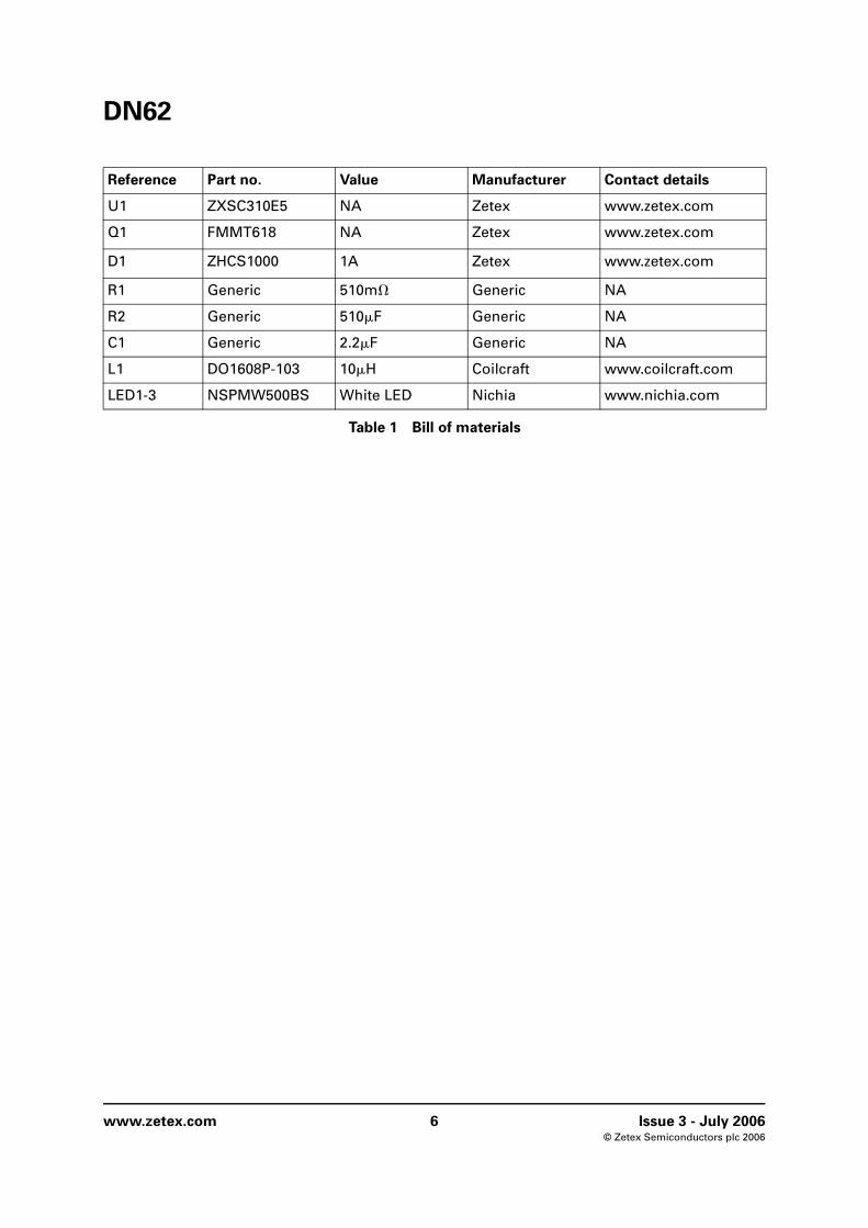
DN62
Reference Part no. Value Manufacturer Contact details
U1 ZXSC310E5 NA Zetex www.zetex.com
Q1 FMMT618 NA Zetex www.zetex.com
D1 ZHCS1000 1A Zetex www.zetex.com
R1 Generic 510m Generic NA
R2 Generic 510F Generic NA
C1 Generic 2.2F Generic NA
L1 DO1608P-103 10H Coilcraft www.coilcraft.com
LED1-3 NSPMW500BS White LED Nichia www.nichia.com
Table 1 Bill of materials
www.zetex.com 6 Issue 3 - July 2006© Zetex Semiconductors plc 2006

DN63
ZXSC310 Solution to drive 8 LEDs connected in series
Description
This solution is optimized for an input voltage range of 4V to 3.5V. The LED current is set toapproximately at 25mA VIN = 4V for 8 white LEDs connected in series.
Figure 1 Schematic diagram
Figure 2 Performance graphs
Issue 4 - July 2006 7 www.zetex.com© Zetex Semiconductors plc 2006

DN63
Reference Part no. Value Manufacturer Contact details
U1 ZXSC310E5 NA Zetex www.zetex.com
Q1 FMMT619 NA Zetex www.zetex.com
D1 ZHCS1000 1A Zetex www.zetex.com
R1 Generic 47m Generic NA
C1 Generic 2.2F Generic NA
L1 DO1608P-683 68H Coilcraft www.coilcraft.com
LED1-8 NSPW500BS White LED Nichia www.nichia.com
Table 1 Bill of materials
www.zetex.com 8 Issue 4 - July 2006© Zetex Semiconductors plc 2006

DN64
ZXSC310 Solution flashlight
Description
A solution is provided for flashlight driving 4 white LEDs connected in series from a 2 alkaline cellinput.
Figure 1 Schematic diagram
Figure 2 Performance graphs
Issue 3 - July 2006 9 www.zetex.com© Zetex Semiconductors plc 2006
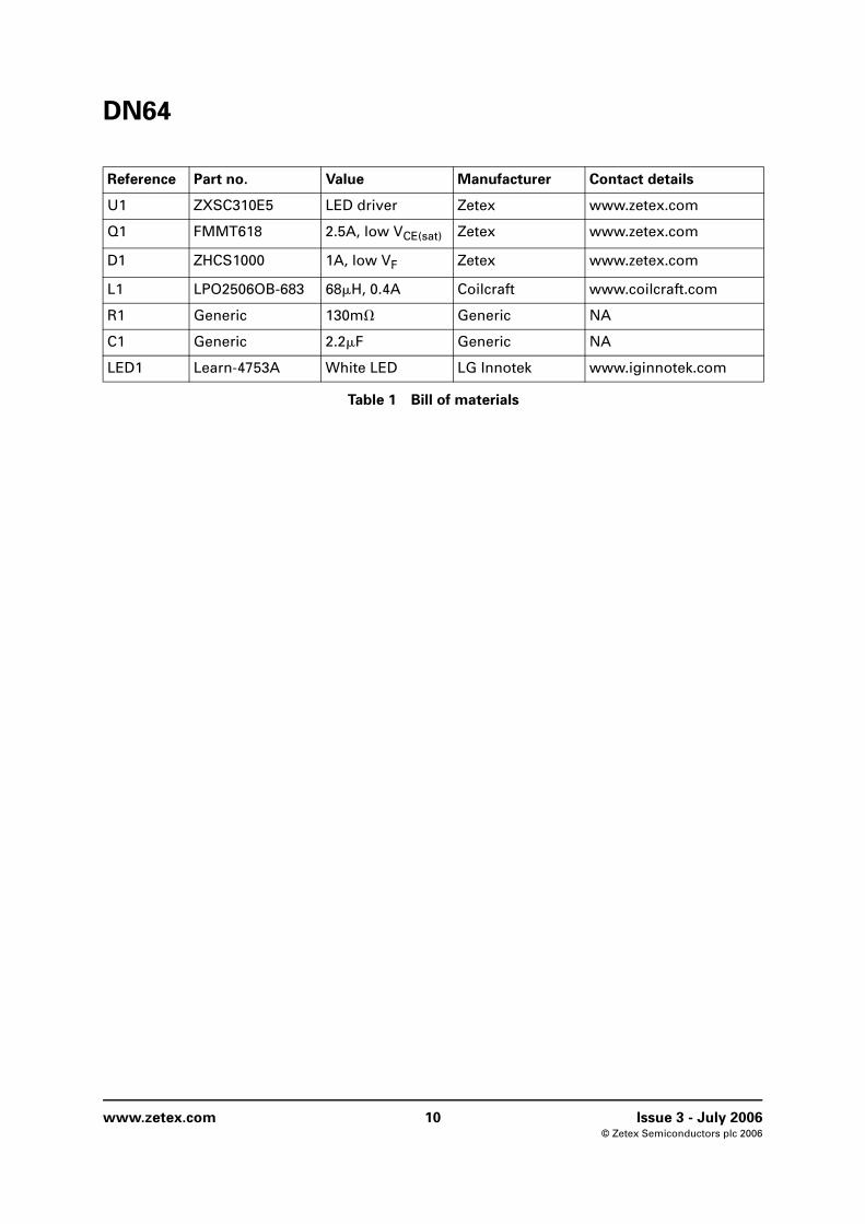
DN64
Reference Part no. Value Manufacturer Contact details
U1 ZXSC310E5 LED driver Zetex www.zetex.com
Q1 FMMT618 2.5A, low VCE(sat) Zetex www.zetex.com
D1 ZHCS1000 1A, low VF Zetex www.zetex.com
L1 LPO2506OB-683 68H, 0.4A Coilcraft www.coilcraft.com
R1 Generic 130m Generic NA
C1 Generic 2.2F Generic NA
LED1 Learn-4753A White LED LG Innotek www.iginnotek.com
Table 1 Bill of materials
www.zetex.com 10 Issue 3 - July 2006© Zetex Semiconductors plc 2006
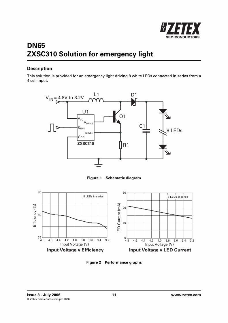
DN65
ZXSC310 Solution for emergency light
Description
This solution is provided for an emergency light driving 8 white LEDs connected in series from a4 cell input.
Figure 1 Schematic diagram
Figure 2 Performance graphs
ZXSC310
Issue 3 - July 2006 11 www.zetex.com© Zetex Semiconductors plc 2006
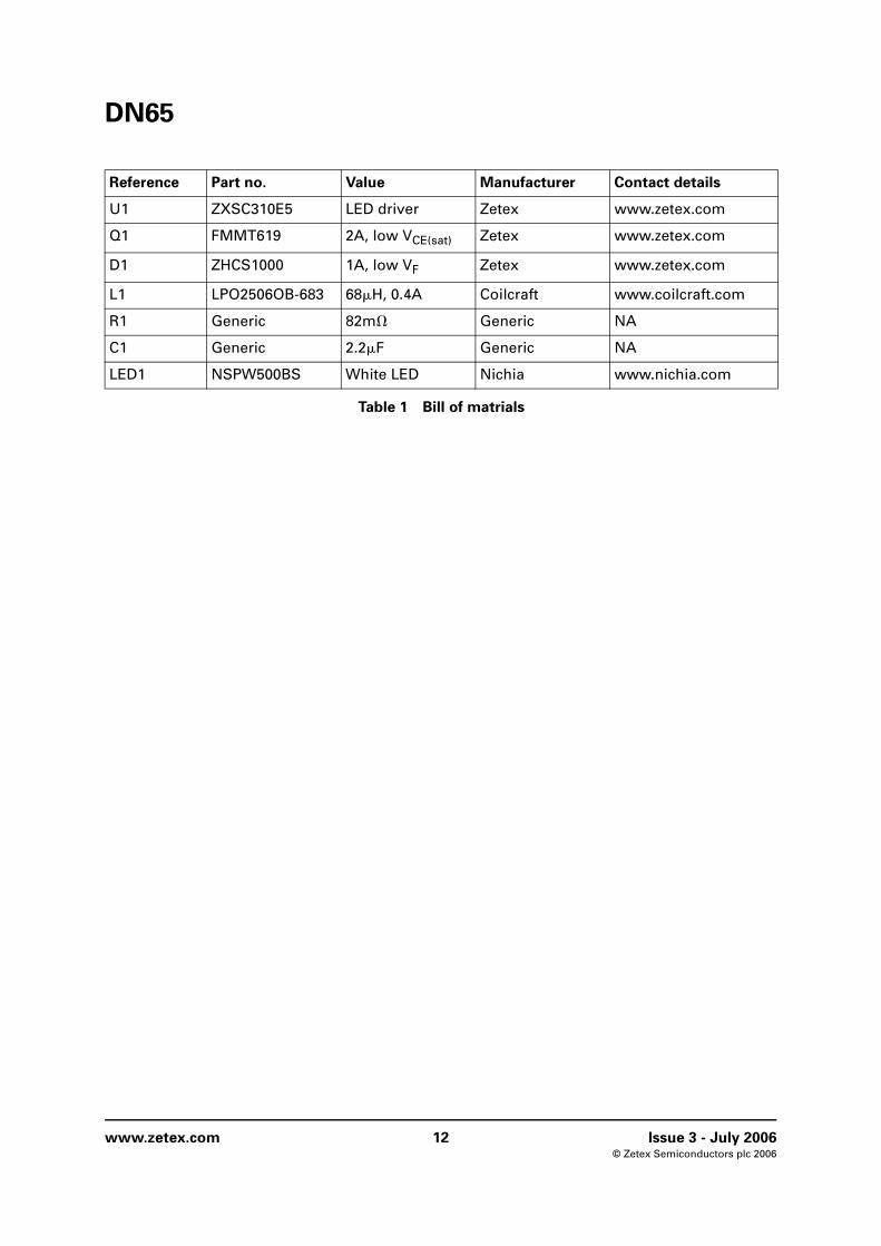
DN65
Reference Part no. Value Manufacturer Contact details
U1 ZXSC310E5 LED driver Zetex www.zetex.com
Q1 FMMT619 2A, low VCE(sat) Zetex www.zetex.com
D1 ZHCS1000 1A, low VF Zetex www.zetex.com
L1 LPO2506OB-683 68H, 0.4A Coilcraft www.coilcraft.com
R1 Generic 82m Generic NA
C1 Generic 2.2F Generic NA
LED1 NSPW500BS White LED Nichia www.nichia.com
Table 1 Bill of matrials
www.zetex.com 12 Issue 3 - July 2006© Zetex Semiconductors plc 2006
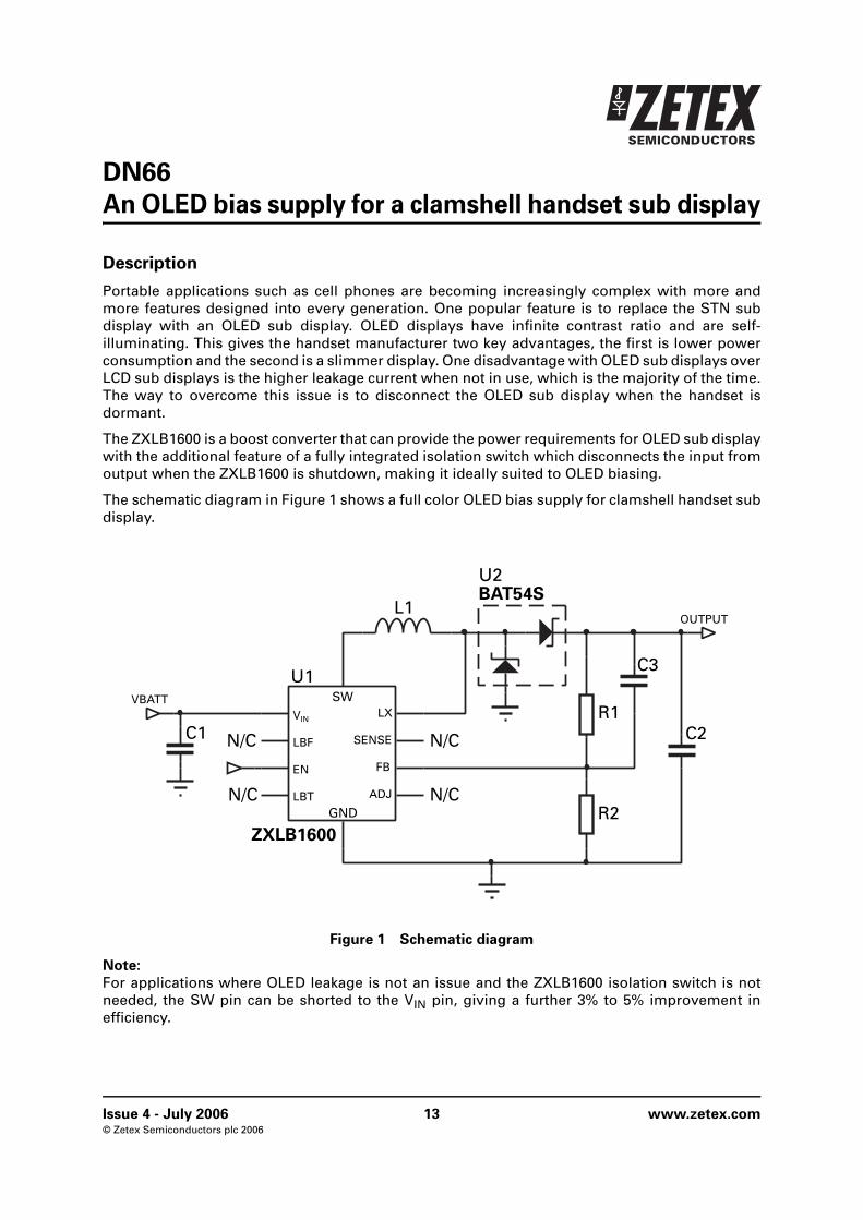
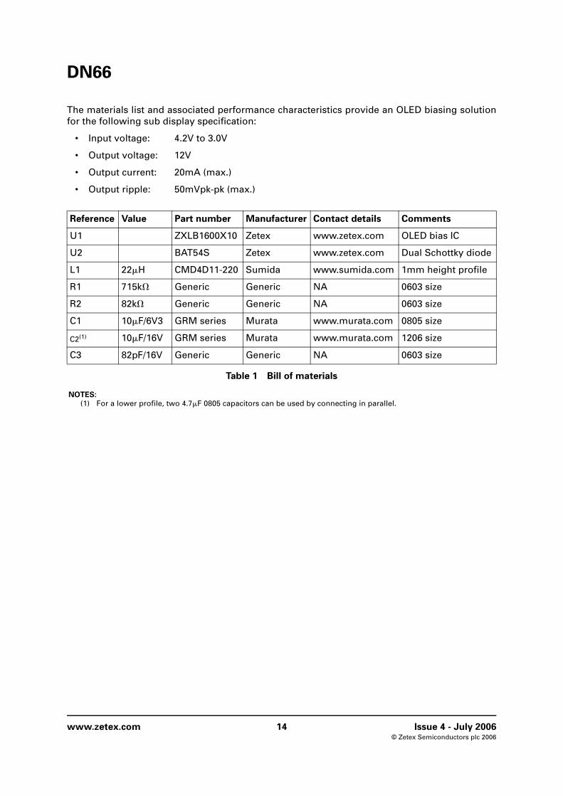
DN66
An OLED bias supply for a clamshell handset sub display
Description
Portable applications such as cell phones are becoming increasingly complex with more andmore features designed into every generation. One popular feature is to replace the STN subdisplay with an OLED sub display. OLED displays have infinite contrast ratio and are self-illuminating. This gives the handset manufacturer two key advantages, the first is lower powerconsumption and the second is a slimmer display. One disadvantage with OLED sub displays overLCD sub displays is the higher leakage current when not in use, which is the majority of the time.The way to overcome this issue is to disconnect the OLED sub display when the handset isdormant.
The ZXLB1600 is a boost converter that can provide the power requirements for OLED sub displaywith the additional feature of a fully integrated isolation switch which disconnects the input fromoutput when the ZXLB1600 is shutdown, making it ideally suited to OLED biasing.
The schematic diagram in Figure 1 shows a full color OLED bias supply for clamshell handset subdisplay.
Figure 1 Schematic diagram
Note:
For applications where OLED leakage is not an issue and the ZXLB1600 isolation switch is notneeded, the SW pin can be shorted to the VIN pin, giving a further 3% to 5% improvement inefficiency.
SWVIN
LBF
EN
LBTGND
ADJ
FB
SENSE
LX
U1
ZXLB1600
L1
C2
OUTPUT
C1
VBATT
U2BAT54S
R1
R2
N/C
N/C N/C
N/C
C3
Issue 4 - July 2006 13 www.zetex.com© Zetex Semiconductors plc 2006
DN66
The materials list and associated performance characteristics provide an OLED biasing solutionfor the following sub display specification:
• Input voltage: 4.2V to 3.0V
• Output voltage: 12V
• Output current: 20mA (max.)
• Output ripple: 50mVpk-pk (max.)
Reference Value Part number Manufacturer Contact details Comments
U1 ZXLB1600X10 Zetex www.zetex.com OLED bias IC
U2 BAT54S Zetex www.zetex.com Dual Schottky diode
L1 22H CMD4D11-220 Sumida www.sumida.com 1mm height profile
R1 715k Generic Generic NA 0603 size
R2 82k Generic Generic NA 0603 size
C1 10F/6V3 GRM series Murata www.murata.com 0805 size
C2(1)
NOTES:
(1) For a lower profile, two 4.7F 0805 capacitors can be used by connecting in parallel.
10F/16V GRM series Murata www.murata.com 1206 size
C3 82pF/16V Generic Generic NA 0603 size
Table 1 Bill of materials
www.zetex.com 14 Issue 4 - July 2006© Zetex Semiconductors plc 2006

DN66
Typical operating characteristics
(For typical application circuit where VIN = 3V, VOUT = 12V, IOUT = 20mA unless otherwise stated)
Figure 2 Performance graphs
Issue 4 - July 2006 15 www.zetex.com© Zetex Semiconductors plc 2006
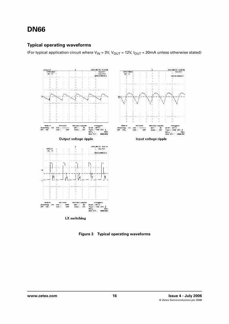
DN66
Typical operating waveforms
(For typical application circuit where VIN = 3V, VOUT = 12V, IOUT = 20mA unless otherwise stated)
Figure 3 Typical operating waveforms
www.zetex.com 16 Issue 4 - July 2006© Zetex Semiconductors plc 2006

DN67
ZXSC400 solution for 1W high powered LEDMike Farley, Field Applications Engineer. December 2003
Description
The ZXSC400, although designed for small LEDs in LCD backlighting, is sufficiently flexible toprovide an efficient 1W solution producing a nominal 350mA constant current source from 2NiMH or NiCd cells.
Figure 1 Schematic diagram
Figure 2 Performance graphs
Issue 3 - July 2006 17 www.zetex.com© Zetex Semiconductors plc 2006

DN67
Figure 3 Open circuit protection
Additional BoM
AD1 - 5V6R3 - 1K
Reference Part number Value Manufacturer Contact details
U1 ZXSC400E6 Zetex www.zetex.com
Q1 FMMT617 Zetex www.zetex.com
D1 ZHCS2000 Zetex www.zetex.com
D2 LXHL-NW98 Lumileds www.lumileds.com
L1 DO1608C-332 3.3H Coilcraft www.coilcraft.com
C1 GRM42-6X5R226K6.3 22F Murata www.murata.com
C2 GRM42-6X5R226K6.3 22F Murata www.murata.com
R1(1)
NOTES:
(1) Actual in-circuit value, see notes overleaf
17m Generic NA
R2 0.82 Generic NA
Table 1 Bill of materials
www.zetex.com 18 Issue 3 - July 2006© Zetex Semiconductors plc 2006

DN67
Figure 4 Layout suggestion
Note
For these approximate layout dimensions, R1 is 15m. See note 3.
Notes:
1. D1 can be exchanged with a SOT23ZHCS1000 with a loss of 5% efficiency.
4. Open circuit protection can be added asshown below. The voltage rating of thesmall signal Zener diode ZD1 is not critical.It must be greater than the maximumforward voltage of the LED and less thanthe maximum VCE rating of the switchingtransistor, 15V in the case of the FMMT617.The supply current in the open circuitcondition is around 2mA.
2. Inductor DCR (DC resistance) stronglyinfluences efficiency, keep below 0.1.
3. R1 is small and it is strongly advised to taketrack resistance into account. A proven method is to source a 1A current from the Sense pin to the GND pin and check for 16-17mV. This resistor can be made from a22m in parallel with a 47m (or a single15m resistor if available) with the PCBtrace contributing the difference.
VIN
U1
L1
C1
C2
Q1
R2
D1
GND
A’ D2
K’ D2
+
+R1
Issue 3 - July 2006 19 www.zetex.com© Zetex Semiconductors plc 2006

DN67
Intentionally left blank
www.zetex.com 20 Issue 3 - July 2006© Zetex Semiconductors plc 2006

DN68
ZXSC310 High power torch reference design
Description
This design note shows a typical ZXSC310 LED driver circuit for a high powered LED torch. Theinput voltage ranges from 0.7V to 1.6V with a maximum output current of 335mA at 1.4V input.
A typical schematic diagram is shown in Figure 1.
Figure 1 Schematic diagram
Reference Value Part number Manufacturer Contact details Comments
U1 ZXSC310E5 Zetex www.zetex.com LED driver in SOT23-5
Q1 FMMT617 Zetex www.zetex.com Low sat. NPN in SOT23
D1 2A ZHCS2000 Zetex www.zetex.com 2A Schottky in SOT23
L1 7.5H DO3316P-153x2 Coilcraft www.coilcraft.com ISAT = 3A
R1 19.5m Generic Generic NA 0805 size
C1 1F Generic Generic NA
C2 220F Generic Generic NA
C3 100F Generic Generic NA
Table 1 Bill of materials
Q1
L1VIN
Vcc
Gnd
Isense
VdriveStdn
U1
ZXSC310
D1
C2
R1
C3C1
Issue 2 - July 2006 21 www.zetex.com© Zetex Semiconductors plc 2006
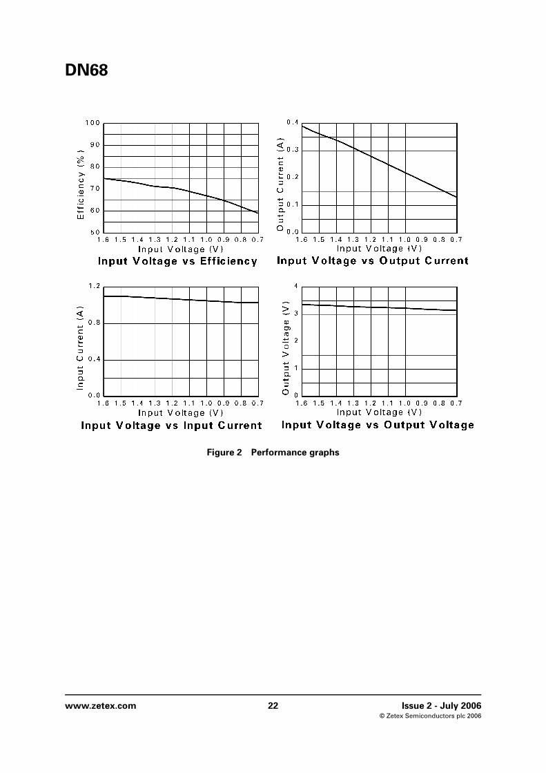
DN68
Figure 2 Performance graphs
www.zetex.com 22 Issue 2 - July 2006© Zetex Semiconductors plc 2006
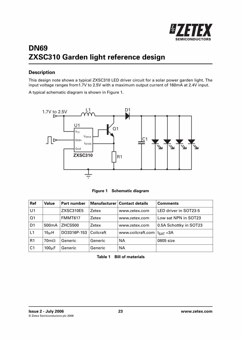
DN69
ZXSC310 Garden light reference design
Description
This design note shows a typical ZXSC310 LED driver circuit for a solar power garden light. Theinput voltage ranges from1.7V to 2.5V with a maximum output current of 160mA at 2.4V input.
A typical schematic diagram is shown in Figure 1.
Figure 1 Schematic diagram
Ref Value Part number Manufacturer Contact details Comments
U1 ZXSC310E5 Zetex www.zetex.com LED driver in SOT23-5
Q1 FMMT617 Zetex www.zetex.com Low sat NPN in SOT23
D1 500mA ZHCS500 Zetex www.zetex.com 0.5A Schottky in SOT23
L1 15H DO3316P-153 Coilcraft www.coilcraft.com ISAT =3A
R1 70m Generic Generic NA 0805 size
C1 100F Generic Generic NA
Table 1 Bill of materials
Q1
L11.7V to 2.5V
VCC
Gnd
ISENSE
VDRIVE
Stdn
U1
ZXSC310
D1
C1
R1
Issue 2 - July 2006 23 www.zetex.com© Zetex Semiconductors plc 2006
DN69
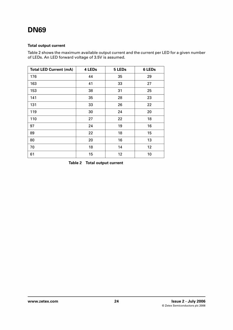
Total output current
Table 2 shows the maximum available output current and the current per LED for a given numberof LEDs. An LED forward voltage of 3.5V is assumed.
Total LED Current (mA) 4 LEDs 5 LEDs 6 LEDs
176 44 35 29
163 41 33 27
153 38 31 25
141 35 28 23
131 33 26 22
119 30 24 20
110 27 22 18
97 24 19 16
89 22 18 15
80 20 16 13
70 18 14 12
61 15 12 10
Table 2 Total output current
www.zetex.com 24 Issue 2 - July 2006© Zetex Semiconductors plc 2006

DN69
Typical operating characteristics
(For typical application circuit where Tamb = 25°C unless otherwise stated)
Figure 2 Performance graphs
Issue 2 - July 2006 25 www.zetex.com© Zetex Semiconductors plc 2006
DN69
Intentionally left blank
www.zetex.com 26 Issue 2 - July 2006© Zetex Semiconductors plc 2006
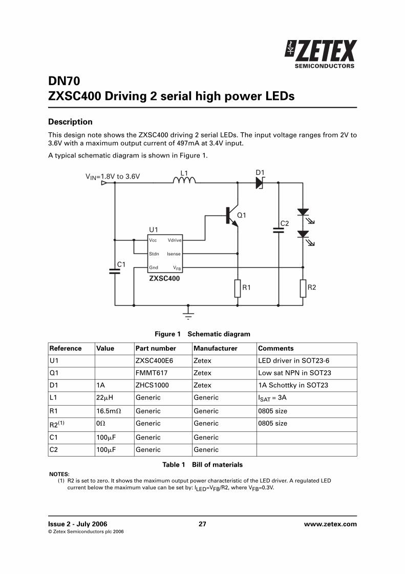
DN70
ZXSC400 Driving 2 serial high power LEDs
Description
This design note shows the ZXSC400 driving 2 serial LEDs. The input voltage ranges from 2V to3.6V with a maximum output current of 497mA at 3.4V input.
A typical schematic diagram is shown in Figure 1.
Figure 1 Schematic diagram
Reference Value Part number Manufacturer Comments
U1 ZXSC400E6 Zetex LED driver in SOT23-6
Q1 FMMT617 Zetex Low sat NPN in SOT23
D1 1A ZHCS1000 Zetex 1A Schottky in SOT23
L1 22H Generic Generic ISAT = 3A
R1 16.5m Generic Generic 0805 size
R2(1)
NOTES:
(1) R2 is set to zero. It shows the maximum output power characteristic of the LED driver. A regulated LED current below the maximum value can be set by: ILED=VFB/R2, where VFB=0.3V.
0 Generic Generic 0805 size
C1 100F Generic Generic
C2 100F Generic Generic
Table 1 Bill of materials
Vcc
Gnd
Isense
Vdrive
Stdn
VFB
U1
ZXSC400
C2
L1VIN=1.8V to 3.6V
C1
R1 R2
Q1
D1
Issue 2 - July 2006 27 www.zetex.com© Zetex Semiconductors plc 2006

DN70
Typical operating characteristics
(For typical application circuit where Tamb = 25°C unless otherwise stated)
Figure 2 Performance graphs
www.zetex.com 28 Issue 2 - July 2006© Zetex Semiconductors plc 2006
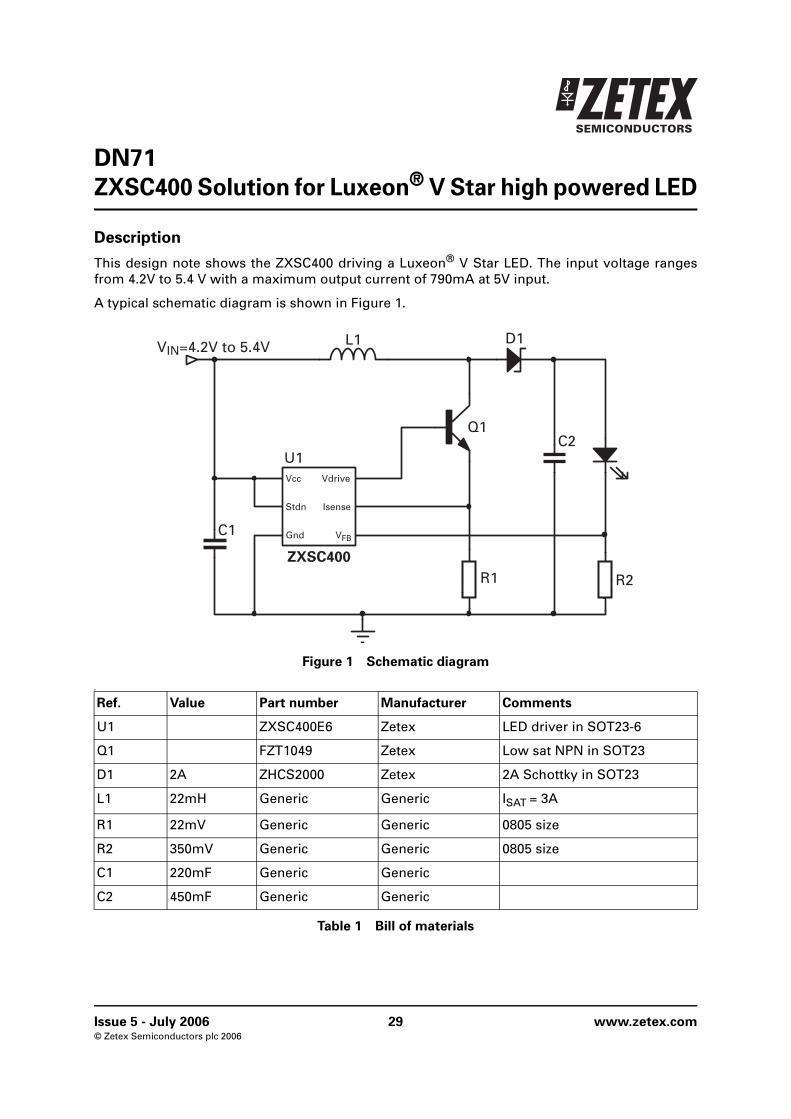
DN71
ZXSC400 Solution for Luxeon® V Star high powered LED
Description
This design note shows the ZXSC400 driving a Luxeon® V Star LED. The input voltage rangesfrom 4.2V to 5.4 V with a maximum output current of 790mA at 5V input.
A typical schematic diagram is shown in Figure 1.
Figure 1 Schematic diagram
#
Ref. Value Part number Manufacturer Comments
U1 ZXSC400E6 Zetex LED driver in SOT23-6
Q1 FZT1049 Zetex Low sat NPN in SOT23
D1 2A ZHCS2000 Zetex 2A Schottky in SOT23
L1 22mH Generic Generic ISAT = 3A
R1 22mV Generic Generic 0805 size
R2 350mV Generic Generic 0805 size
C1 220mF Generic Generic
C2 450mF Generic Generic
Table 1 Bill of materials
Vcc
Gnd
Isense
Vdrive
Stdn
VFB
U1
ZXSC400
C2
L1VIN=4.2V to 5.4V
C1
R1 R2
Q1
D1
Issue 5 - July 2006 29 www.zetex.com© Zetex Semiconductors plc 2006

DN71
Typical operating characteristics
(For typical application circuit where Tamb = 25°C unless otherwise stated)
Figure 2 Performance graphs
www.zetex.com 30 Issue 5 - July 2006© Zetex Semiconductors plc 2006

DN72
ZXLD1101 Driving 8 series LEDs
Description
This design note shows the ZXLD1101 driving 8 series connected LEDs. The input voltage rangesfrom 4.2V to 5.2V with a maximum output current of 24mA at 5V input.
A typical schematic diagram is shown in Figure 1.
Figure 1 Schematic diagram
Ref. Value Part number Manufacturer Comments
U1 ZXLD1101E6 Zetex LED Driver in SOT23-6
D1 1A ZHCS1000 Zetex 1A Schottky in SOT23
L1 33H Generic Generic
R1(1)
NOTES:
(1) R1 is set to zero. It shows the maximum output power characteristic of the LED driver. A regulated LED current below the maximum value can be set by: ILED = VFB/R1, where VFB = 0.1V.
0 Generic Generic 0805 size
C1 100F Generic Generic
C2 1F Generic Generic
C3 10F Generic Generic
Table 1 Bill of materials
L1 D1
R1
C3
EN
GND
FB
LXVIN
ZXLD1101
x8 LEDs
C2
C1
VIN
Issue 2 - July 2006 31 www.zetex.com© Zetex Semiconductors plc 2006

DN72
Typical operating characteristics
(For typical application circuit where Tamb = 25°C unless otherwise stated)
Figure 2 Performance graphs
www.zetex.com 32 Issue 2 - July 2006© Zetex Semiconductors plc 2006
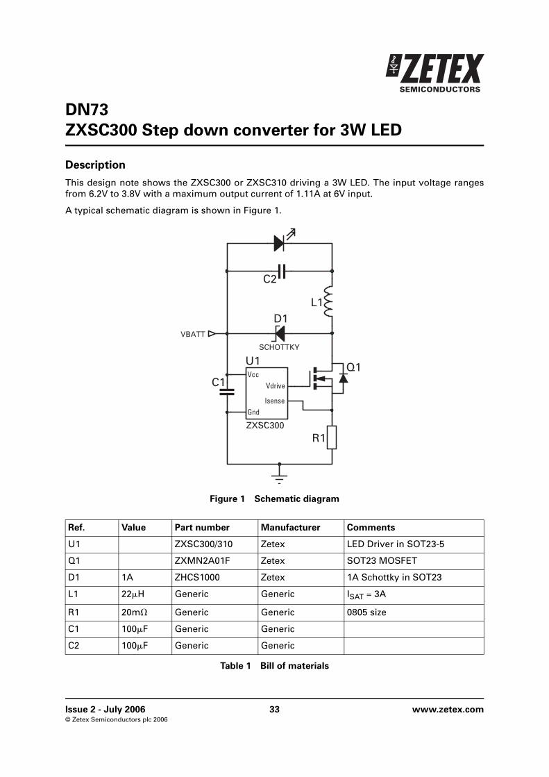
DN73
ZXSC300 Step down converter for 3W LED
Description
This design note shows the ZXSC300 or ZXSC310 driving a 3W LED. The input voltage rangesfrom 6.2V to 3.8V with a maximum output current of 1.11A at 6V input.
A typical schematic diagram is shown in Figure 1.
Figure 1 Schematic diagram
Ref. Value Part number Manufacturer Comments
U1 ZXSC300/310 Zetex LED Driver in SOT23-5
Q1 ZXMN2A01F Zetex SOT23 MOSFET
D1 1A ZHCS1000 Zetex 1A Schottky in SOT23
L1 22H Generic Generic ISAT = 3A
R1 20m Generic Generic 0805 size
C1 100F Generic Generic
C2 100F Generic Generic
Table 1 Bill of materials
Issue 2 - July 2006 33 www.zetex.com© Zetex Semiconductors plc 2006
DN73
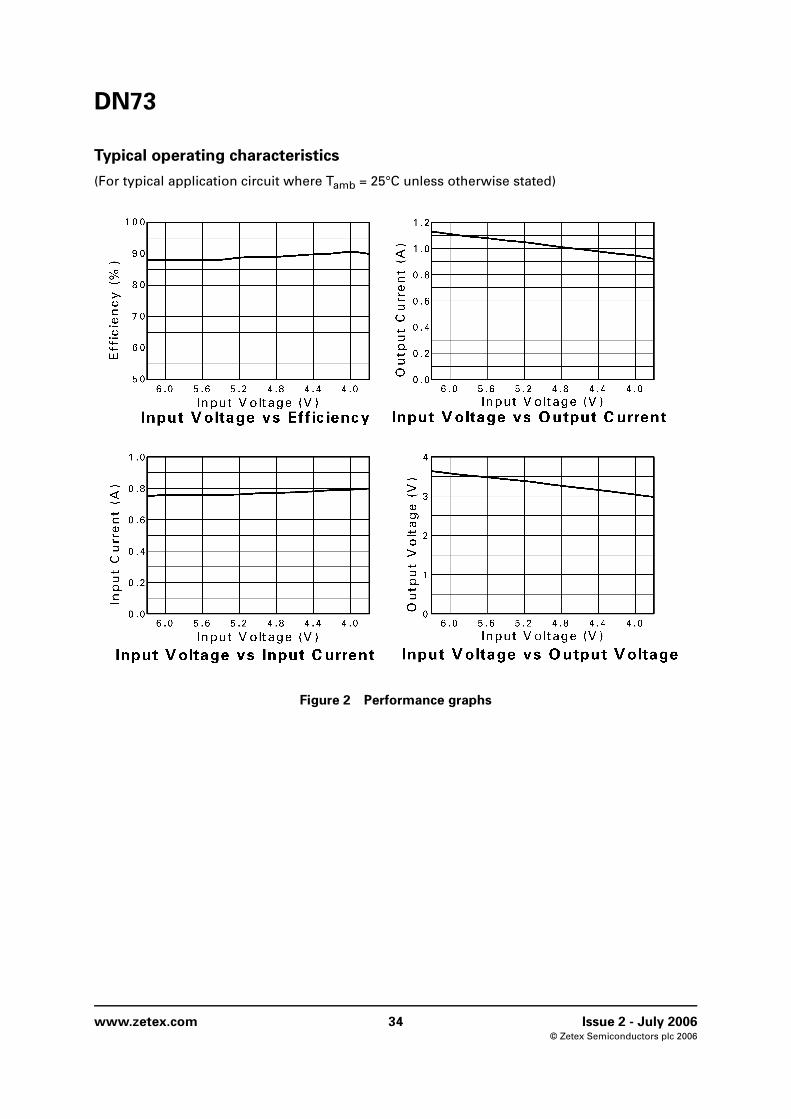
Typical operating characteristics
(For typical application circuit where Tamb = 25°C unless otherwise stated)
Figure 2 Performance graphs
www.zetex.com 34 Issue 2 - July 2006© Zetex Semiconductors plc 2006

DN74
ZXSC400 Photoflash LED reference design
Description
This design note shows the ZXSC400 driving a Photoflash LED. The input voltage is 3V with amaximum pulsed output current of 1A for 2ms.
A typical schematic diagram is shown in Figure 1.
Figure 1 Schematic diagram
Operation
In charging mode, SW1 is closed and SW2 is open the ZXSC400 is configured as a typical boostconverter, charging capacitor C2 up the regulated output voltage set by the ratio of R1 and R2.This is typically 16V. The peak current of the converter (current drawn from the battery) iscontrolled by R3 plus R4, and is typically 280mA for this application. When C2 is charged to 16Vthe SW1 is opened and SW2 is closed, converting the ZXSC400 to a step down converter toprovide a 1A constant current for 2ms to the photoflash LED. During step down operation, currentflows from C2, through the photoflash LED, L1, U2 and is returned to C2 through R3. This meansthat the peak current is set at a higher value than in charging mode, typically 1A. When the currentreaches it's peak value, U2 is switched off and current flows from L1 through the Schottky diodein U2, to the photoflash LED. This cyclic process is repeated until C2 is discharged.
VCC
GND
ISENSE
VDRIVE
STDN
VFB
U1
ZXSC400
C2
L1
VBATT
C1 R3
R1
R4
R2
C3
SW2
SW1
Charging mode: SW1 closed, SW2 openDischarging mode: SW1 open, SW2 closed
U2
Issue 2 - July 2006 35 www.zetex.com© Zetex Semiconductors plc 2006

DN74
Typical operating waveforms
(For typical application circuit where VBATT = 3V and Tamb = 25°C unless otherwise stated)
Figure 2 Performance graphs
Ref Value Part number Manufacturer Comments
U1 ZXSC400E6 Zetex LED Driver in SOT23-6
U2 ZX3CDBS1M832 Zetex Dual NPN and Schottky
L1 12H Generic Generic ISAT=1A
R1 10k Generic Generic 0805 size
R2 510k Generic Generic 0805 size
R3 22m Generic Generic 0805 size
R4 100m Generic Generic 0805 size
C1 1F Generic Generic
C2 150F Generic Generic
C3 1F Generic Generic
Table 1 Bill of materials
www.zetex.com 36 Issue 2 - July 2006© Zetex Semiconductors plc 2006
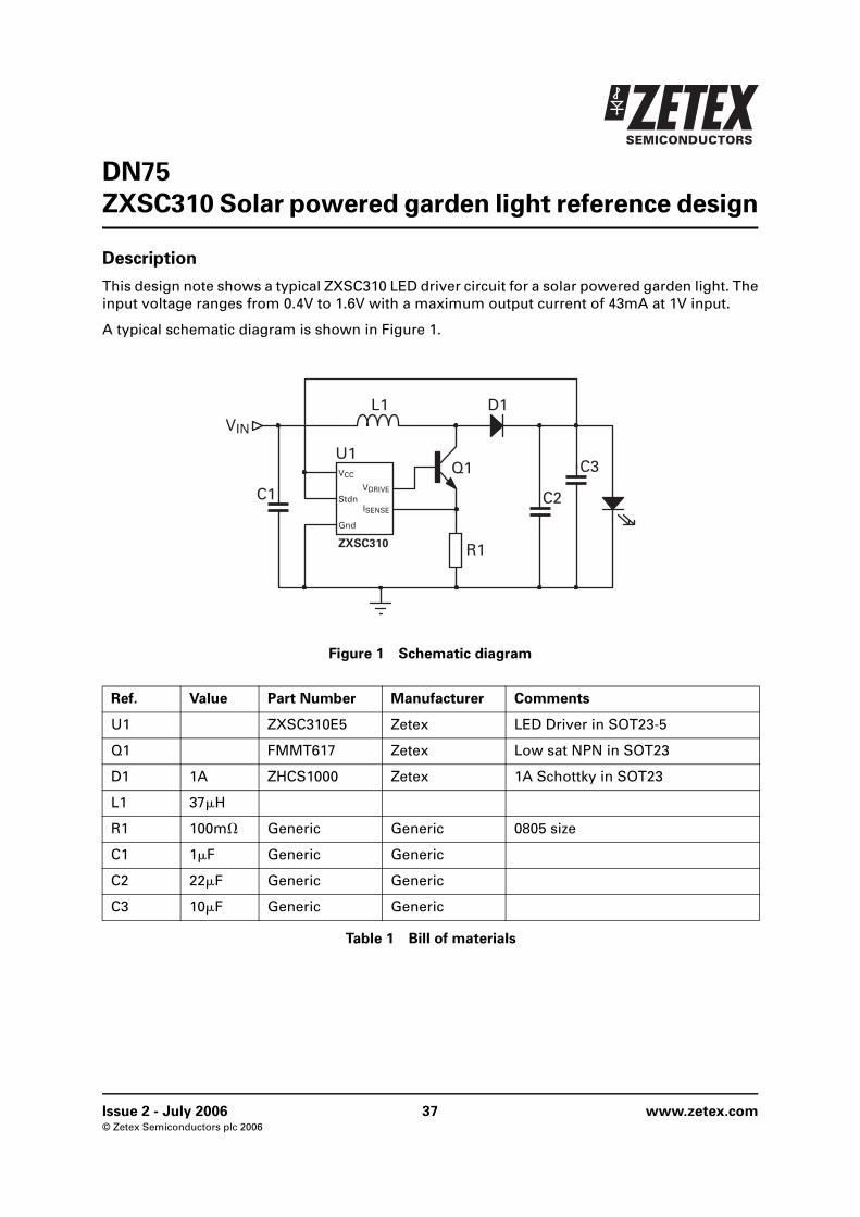
DN75
ZXSC310 Solar powered garden light reference design
Description
This design note shows a typical ZXSC310 LED driver circuit for a solar powered garden light. Theinput voltage ranges from 0.4V to 1.6V with a maximum output current of 43mA at 1V input.
A typical schematic diagram is shown in Figure 1.
Figure 1 Schematic diagram
Ref. Value Part Number Manufacturer Comments
U1 ZXSC310E5 Zetex LED Driver in SOT23-5
Q1 FMMT617 Zetex Low sat NPN in SOT23
D1 1A ZHCS1000 Zetex 1A Schottky in SOT23
L1 37H
R1 100m Generic Generic 0805 size
C1 1F Generic Generic
C2 22F Generic Generic
C3 10F Generic Generic
Table 1 Bill of materials
Q1
L1VIN
VCC
Gnd
ISENSE
VDRIVEStdn
U1
ZXSC310
D1
C2
R1
C3
C1
Issue 2 - July 2006 37 www.zetex.com© Zetex Semiconductors plc 2006
DN75
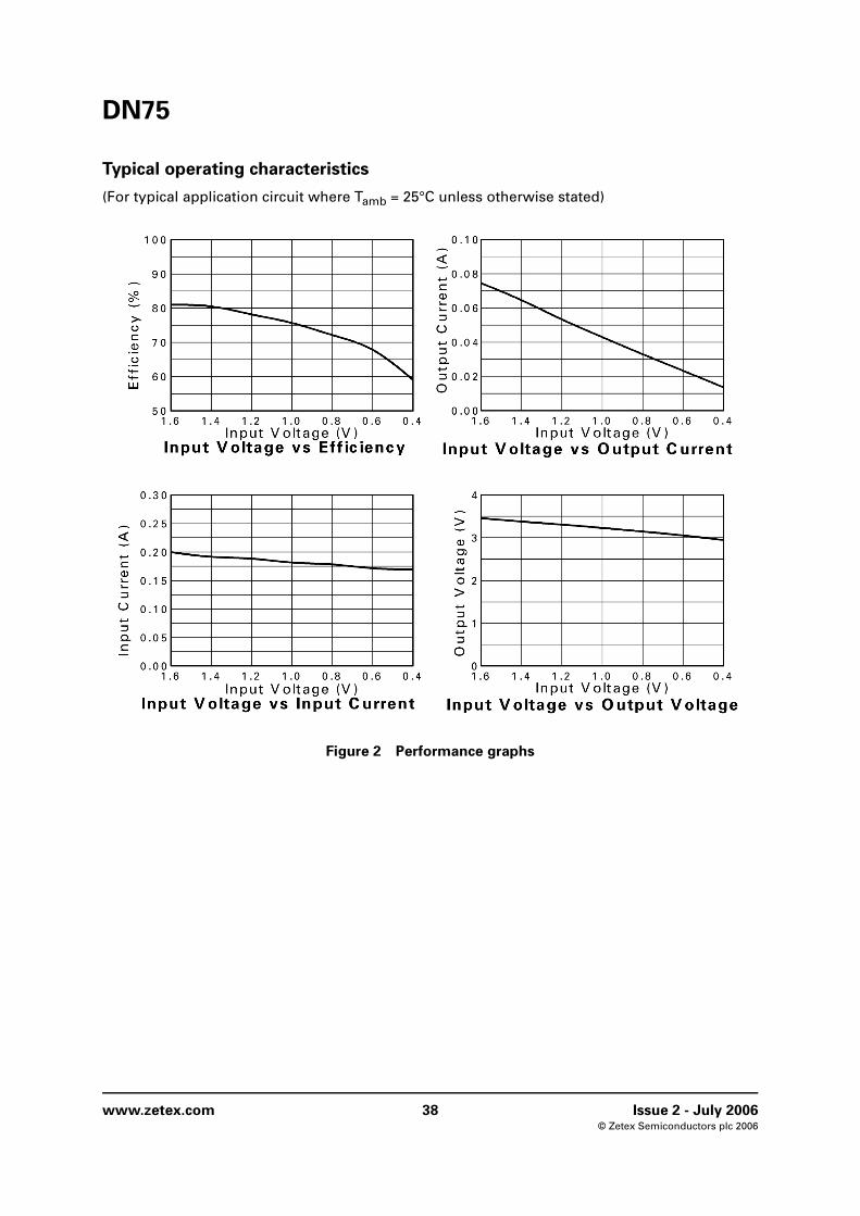
Typical operating characteristics
(For typical application circuit where Tamb = 25°C unless otherwise stated)
Figure 2 Performance graphs
www.zetex.com 38 Issue 2 - July 2006© Zetex Semiconductors plc 2006
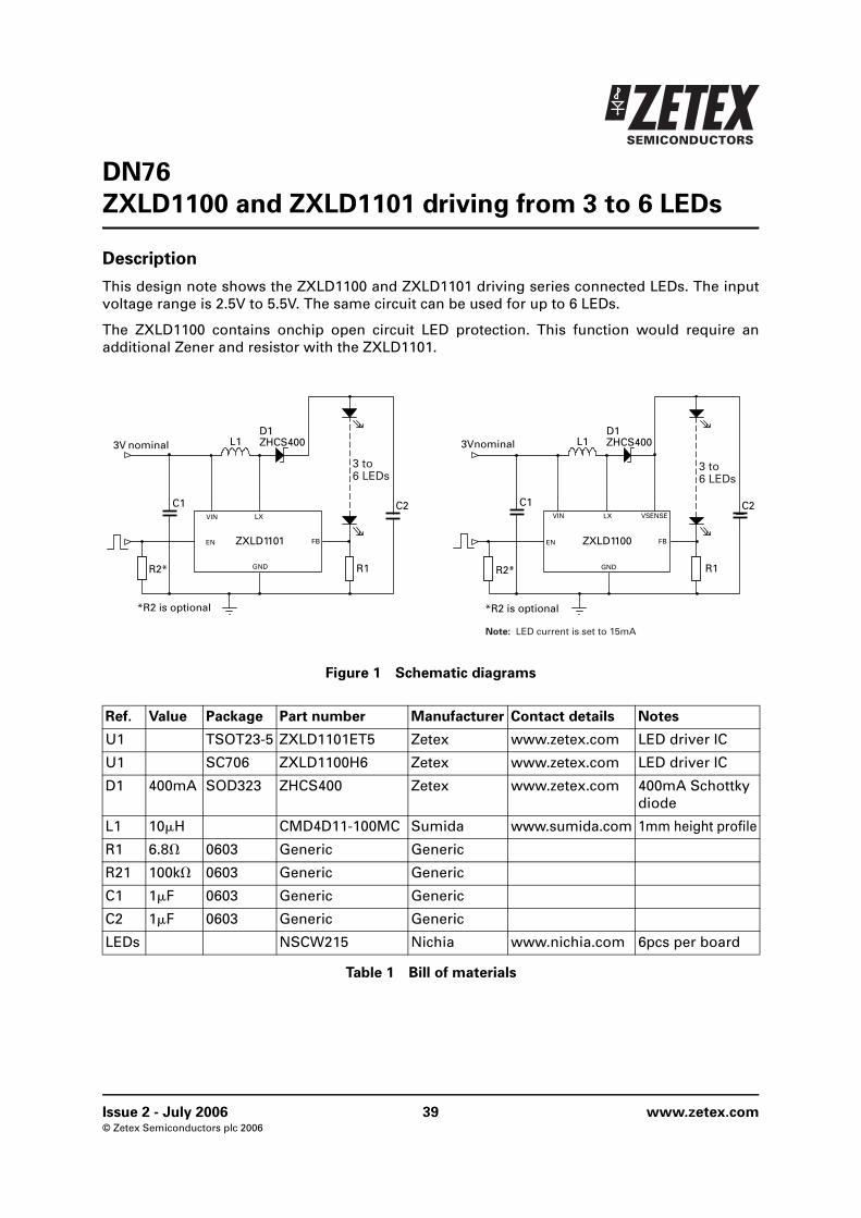
DN76
ZXLD1100 and ZXLD1101 driving from 3 to 6 LEDs
Description
This design note shows the ZXLD1100 and ZXLD1101 driving series connected LEDs. The inputvoltage range is 2.5V to 5.5V. The same circuit can be used for up to 6 LEDs.
The ZXLD1100 contains onchip open circuit LED protection. This function would require anadditional Zener and resistor with the ZXLD1101.
Figure 1 Schematic diagrams
Ref. Value Package Part number Manufacturer Contact details Notes
U1 TSOT23-5 ZXLD1101ET5 Zetex www.zetex.com LED driver IC
U1 SC706 ZXLD1100H6 Zetex www.zetex.com LED driver IC
D1 400mA SOD323 ZHCS400 Zetex www.zetex.com 400mA Schottky diode
L1 10H CMD4D11-100MC Sumida www.sumida.com 1mm height profile
R1 6.8 0603 Generic Generic
R21 100k 0603 Generic Generic
C1 1F 0603 Generic Generic
C2 1F 0603 Generic Generic
LEDs NSCW215 Nichia www.nichia.com 6pcs per board
Table 1 Bill of materials
Note: LED current is set to 15mA
Issue 2 - July 2006 39 www.zetex.com© Zetex Semiconductors plc 2006

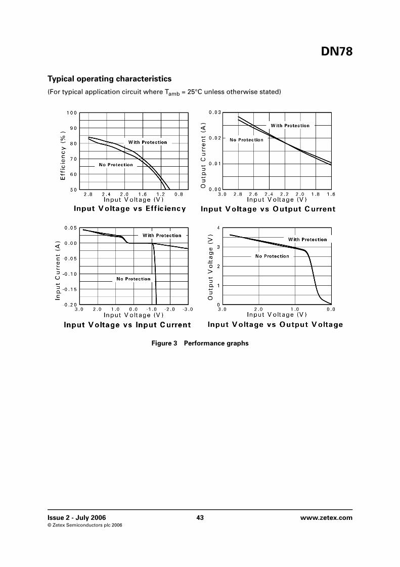
DN76
Typical operating characteristics
(For typical application circuit where Tamb = 25°C unless otherwise stated)
Figure 2 Performance graphs
www.zetex.com 40 Issue 2 - July 2006© Zetex Semiconductors plc 2006

DN78
ZXSC310 with reverse polarity protection
Description
The Schematic diagram shown in Figure 1 is a typical example of the ZXSC310 used in a LEDflashlight application. The input voltage can either be one or two alkaline cells. If the battery is putin the flashlight the wrong way, the reverse polarity can damage the ZXSC310 and switchingtransistor, Q1. Implementing a mechanical reverse protection method can be expensive, and notalways reliable. This paper describes methods of electronic reverse protection, without efficiencyloss, for the ZXSC series ICs and related LED flashlight application circuits.
Circuit problems caused by the reverse polarity battery
If a negative voltage appears at the input terminal of Figure 1 then reverse current will flow fromthe ground pin of the ZXSC310 to the VCC terminal and back to battery. This current is high andwill damage the ZXSC310. Some of this reverse current will also flow through the VDRIVE terminalof the ZXSC310 and into Q1 base-collector completing the circuit to the battery.
The reverse current through base-collector of Q1 turns the transistor on in the reverse directionand causes high current to flow from ground, through emitter-collector and to the batteryresulting in battery drainage and possible damage to the switching transistor, Q1.
A common method of reverse polarity protection
A common method of reverse protection is to add a Schottky diode in series with the batterypositive. The problem with this method of reverse protection is that there is a loss of efficiencydue to the forward voltage drop of the diode, typically 5% to 10% depending upon input voltage,reducing the usable battery life. The proposed method of reverse protection for the ZXSC seriesIC's gives full protection with NO loss of efficiency.
Figure 1 Schematic diagram
Issue 2 - July 2006 41 www.zetex.com© Zetex Semiconductors plc 2006

DN78
Reverse protection without efficiency loss
By adding current limiting resistor and Schottky diode, the reverse current flow can be eliminatedwithout a loss of efficiency.
Torch circuit with bootstrap
For the bootstrap circuit in Figure 2, the current through the ZXSC310 is blocked by the reversedbiased Schottky diode, D1.
The current from VDRIVE, which turns on Q1 in the reverse direction, is diverted via D2, throughL1 and back to the battery so that Q1 does not turn on. R2 is a current limiting resistor to controlthis VDRIVE current. This value is typically set to 100V to 500V to minimize battery current drainwithout affecting the normal operation of the circuit.
Figure 2
Ref Value Part number Manufacturer Comments
U1 ZXSC310E5 Zetex LED driver in SOT23-5
Q1 FMMT617 Zetex Low sat NPN in SOT23
D1 1A ZHCS1000 Zetex 1A Schottky in SOT23
D2(1)
NOTES:
(1) Add for reverse protection
1A ZHCS1000 Zetex 1A Schottky in SOT23
L1 72H Generic Generic ISAT>0.5A, R<0.3
R1 260m Generic Generic 0805 size
R2(1) 100 Generic Generic 0805 size
C1 10F Generic Generic
C2 22F Generic Generic
Table 1 Bill of materials
www.zetex.com 42 Issue 2 - July 2006© Zetex Semiconductors plc 2006
DN78
Typical operating characteristics
(For typical application circuit where Tamb = 25°C unless otherwise stated)
Figure 3 Performance graphs
Issue 2 - July 2006 43 www.zetex.com© Zetex Semiconductors plc 2006
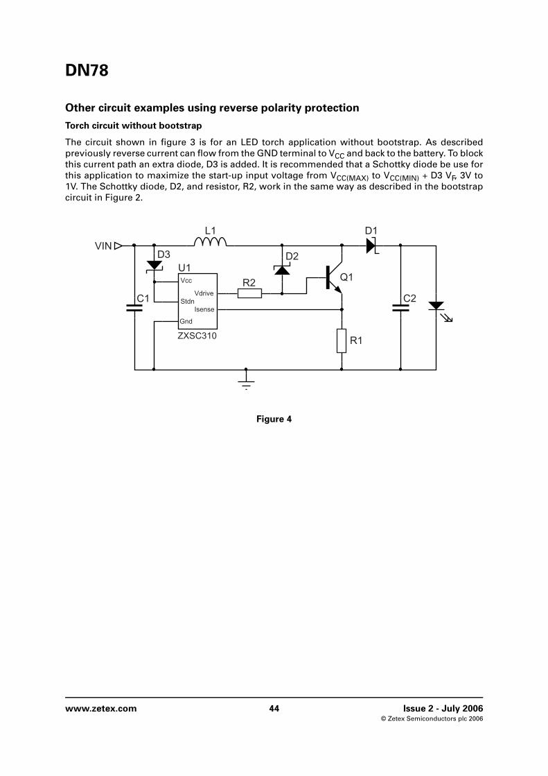
DN78
Other circuit examples using reverse polarity protection
Torch circuit without bootstrap
The circuit shown in figure 3 is for an LED torch application without bootstrap. As describedpreviously reverse current can flow from the GND terminal to VCC and back to the battery. To blockthis current path an extra diode, D3 is added. It is recommended that a Schottky diode be use forthis application to maximize the start-up input voltage from VCC(MAX) to VCC(MIN) + D3 VF, 3V to1V. The Schottky diode, D2, and resistor, R2, work in the same way as described in the bootstrapcircuit in Figure 2.
Figure 4
www.zetex.com 44 Issue 2 - July 2006© Zetex Semiconductors plc 2006
DN78
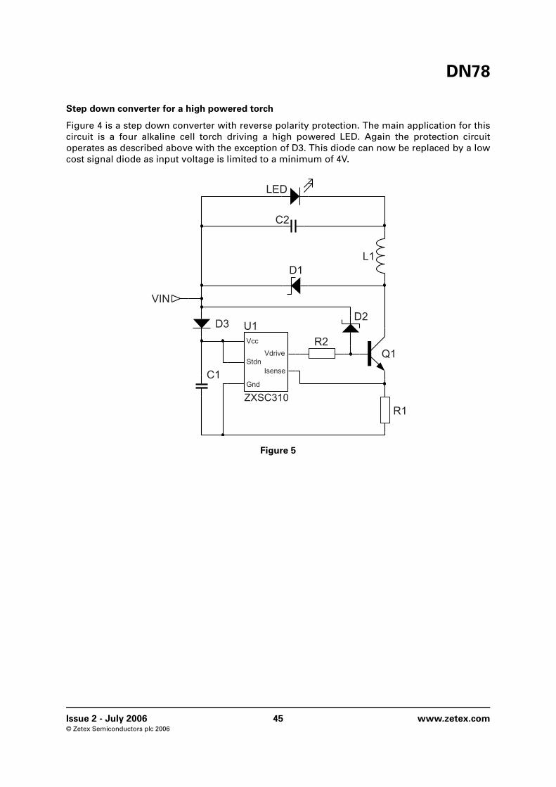
Step down converter for a high powered torch
Figure 4 is a step down converter with reverse polarity protection. The main application for thiscircuit is a four alkaline cell torch driving a high powered LED. Again the protection circuitoperates as described above with the exception of D3. This diode can now be replaced by a lowcost signal diode as input voltage is limited to a minimum of 4V.
Figure 5
Issue 2 - July 2006 45 www.zetex.com© Zetex Semiconductors plc 2006

DN78
Intentionally left blank
www.zetex.com 46 Issue 2 - July 2006© Zetex Semiconductors plc 2006
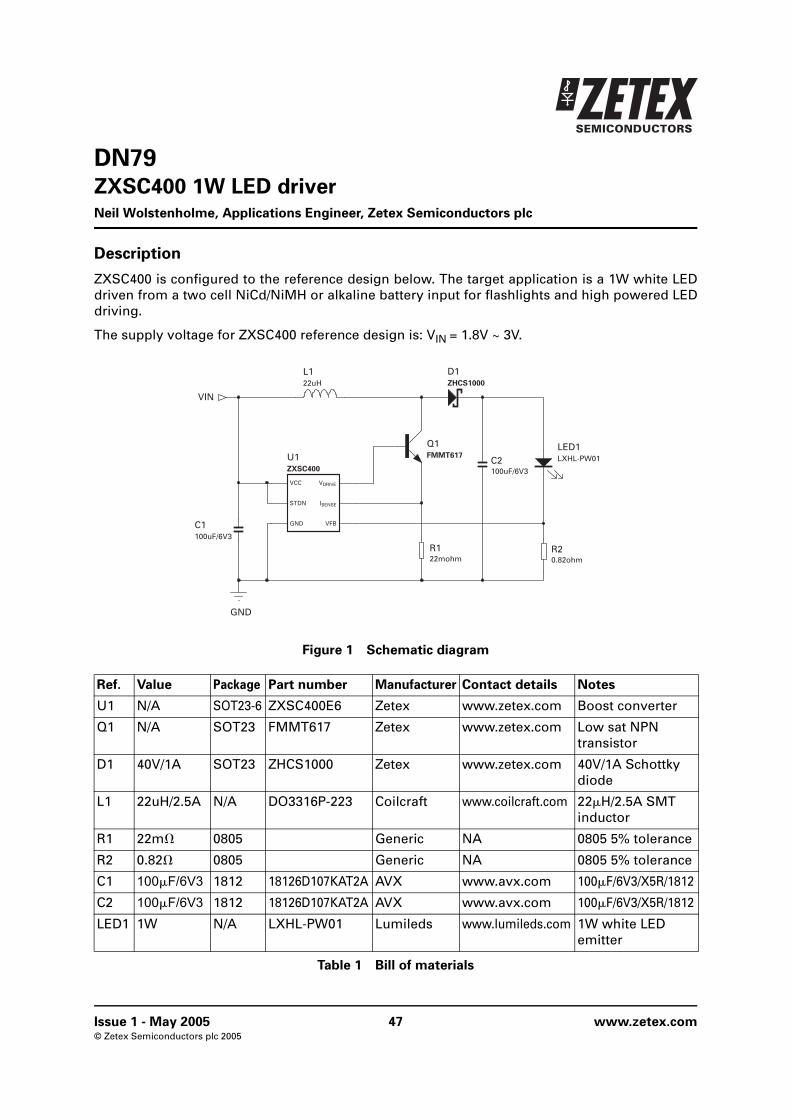
DN79
ZXSC400 1W LED driverNeil Wolstenholme, Applications Engineer, Zetex Semiconductors plc
Description
ZXSC400 is configured to the reference design below. The target application is a 1W white LEDdriven from a two cell NiCd/NiMH or alkaline battery input for flashlights and high powered LEDdriving.
The supply voltage for ZXSC400 reference design is: VIN = 1.8V ~ 3V.
Figure 1 Schematic diagram
Table 1 Bill of materials
Ref. Value Package Part number Manufacturer Contact details Notes
U1 N/A SOT23-6 ZXSC400E6 Zetex www.zetex.com Boost converter
Q1 N/A SOT23 FMMT617 Zetex www.zetex.com Low sat NPN transistor
D1 40V/1A SOT23 ZHCS1000 Zetex www.zetex.com 40V/1A Schottky diode
L1 22uH/2.5A N/A DO3316P-223 Coilcraft www.coilcraft.com 22H/2.5A SMT inductor
R1 22m 0805 Generic NA 0805 5% tolerance
R2 0.82 0805 Generic NA 0805 5% tolerance
C1 100F/6V3 1812 18126D107KAT2A AVX www.avx.com 100F/6V3/X5R/1812
C2 100F/6V3 1812 18126D107KAT2A AVX www.avx.com 100F/6V3/X5R/1812
LED1 1W N/A LXHL-PW01 Lumileds www.lumileds.com 1W white LED emitter
VCC
GND
ISENSE
VDRIVE
STDN
VFB
U1ZXSC400
C2100uF/6V3
L122uH
C1100uF/6V3
Q1FMMT617
D1ZHCS1000
VIN
GND
R20.82ohm
LED1LXHL-PW01
R122mohm
Issue 1 - May 2005 47 www.zetex.com© Zetex Semiconductors plc 2005

DN79
Performance
Increasing efficiency
On ZXSC400 reference design, R1 is set to 22mΩ to ensure that the LED current is regulated overthe full input voltage range of 3V ~ 1.8V. For improved efficiency R1 can be changed to a 33mΩresistor but LED current will not be regulated below 2V. See Figure 2, Performance graphs.
Figure 2 Performance graphs
3.0 2.8 2.6 2.4 2.2 2.0 1.850
60
70
80
90
100
3.0 2.8 2.6 2.4 2.2 2.0 1.8300
320
340
360
380
400
3.0 2.8 2.6 2.4 2.2 2.0 1.83.0
3.2
3.4
3.6
3.8
4.0
3.0 2.8 2.6 2.4 2.2 2.0 1.8400
600
800
1000
R1=22mohms
R1=22mohmsR1=33mohms
R1=22mohms
LED Current vs Input Voltage
VIN
I =350mA
Eff
icie
ncy
(%
)
Input voltage (V)
R1=33mohms
LED Voltage vs Input Voltage
LED
Cu
rren
t (m
A)
Input Voltage (V)
R1=33mohms
V
Efficiency vs Input Voltage
LED
Vo
ltag
e (V
)
Input Voltage (V)
R1=33mohms
R1=22mohms
Input Current vs Input Voltage
Inp
ut
Cu
rren
t (m
A)
Input Voltage (V)
STDN
LED
=V VSTDN
=VIN
STDN=V
INV
STDN=V
IN
www.zetex.com 48 Issue 1 - May 2005© Zetex Semiconductors plc 2005
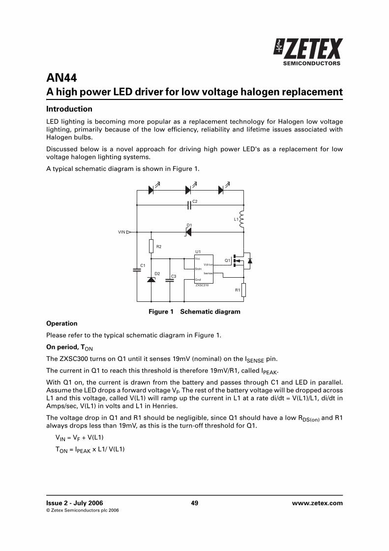
AN44
A high power LED driver for low voltage halogen replacement
Introduction
LED lighting is becoming more popular as a replacement technology for Halogen low voltagelighting, primarily because of the low efficiency, reliability and lifetime issues associated withHalogen bulbs.
Discussed below is a novel approach for driving high power LED's as a replacement for lowvoltage halogen lighting systems.
A typical schematic diagram is shown in Figure 1.
Figure 1 Schematic diagram
Operation
Please refer to the typical schematic diagram in Figure 1.
On period, TON
The ZXSC300 turns on Q1 until it senses 19mV (nominal) on the ISENSE pin.
The current in Q1 to reach this threshold is therefore 19mV/R1, called IPEAK.
With Q1 on, the current is drawn from the battery and passes through C1 and LED in parallel.Assume the LED drops a forward voltage VF. The rest of the battery voltage will be dropped acrossL1 and this voltage, called V(L1) will ramp up the current in L1 at a rate di/dt = V(L1)/L1, di/dt inAmps/sec, V(L1) in volts and L1 in Henries.
The voltage drop in Q1 and R1 should be negligible, since Q1 should have a low RDS(on) and R1always drops less than 19mV, as this is the turn-off threshold for Q1.
VIN = VF + V(L1)
TON = IPEAK x L1/ V(L1)
Issue 2 - July 2006 49 www.zetex.com© Zetex Semiconductors plc 2006
AN44
So TON can be calculated, as the voltage across L1 is obtained by subtracting the forward LEDvoltage drop from VIN. Therefore, if L1 is smaller, TON will be smaller for the same peak currentIPEAK and the same battery voltage VIN. Note that, while the inductor current is ramping up toIPEAK, the current is flowing through the LED and so the average current in the LED is the sum ofthe ramps during the TON ramping up period and the TOFF ramping down period.
Off period, TOFF
The TOFF of ZXSC300 and ZXSC310 is fixed internally at nominally 1.7µs. Note that, if relying onthis for current ramp calculations, the limits are 1.2µs min., 3.2µs max.
In order to minimize the conductive loss and switching loss, TON should not be much smaller thanTOFF. Very high switching frequencies cause high dv/dt and it is recommended that the ZXSC300and 310 are operated only up to 200 kHz. Given the fixed TOFF of 1.7µs, this gives a TON of (5µs -1.7µs) = 3.3µs minimum. However, this is not an absolute limitation and these devices have beenoperated at 2 or 3 times this frequency, but conversion efficiency can suffer under theseconditions.
During TOFF, the energy stored in the inductor will be transferred to the LED, with some loss in theSchottky diode. The energy stored in the inductor is:
½ x L x IPEAK2 [Joules]
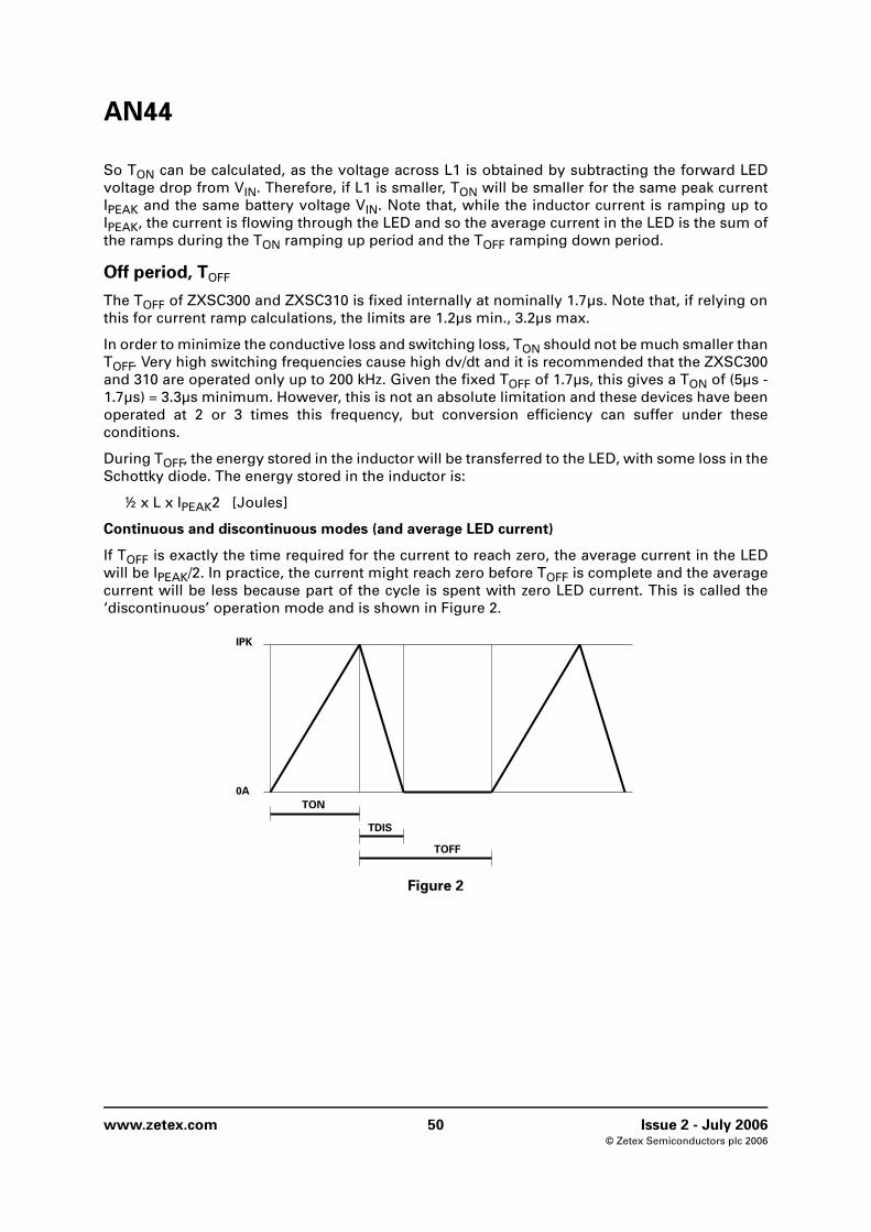
Continuous and discontinuous modes (and average LED current)
If TOFF is exactly the time required for the current to reach zero, the average current in the LEDwill be IPEAK/2. In practice, the current might reach zero before TOFF is complete and the averagecurrent will be less because part of the cycle is spent with zero LED current. This is called the‘discontinuous’ operation mode and is shown in Figure 2.
Figure 2
www.zetex.com 50 Issue 2 - July 2006© Zetex Semiconductors plc 2006
AN44
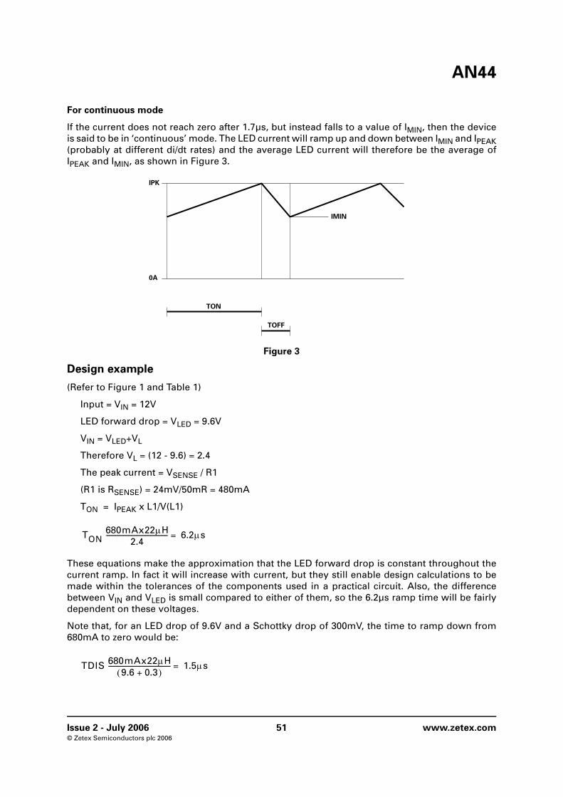
For continuous mode
If the current does not reach zero after 1.7µs, but instead falls to a value of IMIN, then the deviceis said to be in ‘continuous’ mode. The LED current will ramp up and down between IMIN and IPEAK(probably at different di/dt rates) and the average LED current will therefore be the average ofIPEAK and IMIN, as shown in Figure 3.
Figure 3
Design example
(Refer to Figure 1 and Table 1)
Input = VIN = 12V
LED forward drop = VLED = 9.6V
VIN = VLED+VL
Therefore VL = (12 - 9.6) = 2.4
The peak current = VSENSE / R1
(R1 is RSENSE) = 24mV/50mR = 480mA
TON = IPEAK x L1/V(L1)
These equations make the approximation that the LED forward drop is constant throughout thecurrent ramp. In fact it will increase with current, but they still enable design calculations to bemade within the tolerances of the components used in a practical circuit. Also, the differencebetween VIN and VLED is small compared to either of them, so the 6.2µs ramp time will be fairlydependent on these voltages.
Note that, for an LED drop of 9.6V and a Schottky drop of 300mV, the time to ramp down from680mA to zero would be:
TON680mAx22µH
2.4--------------------------------------- 6.2µs=
TDIS 680mAx22µH9.6 0.3+( )
--------------------------------------- 1.5µs=
Issue 2 - July 2006 51 www.zetex.com© Zetex Semiconductors plc 2006
AN44
As the TOFF period is nominally 1.7µs, the current should have time to reach zero. However, 1.5µsis rather close to 1.7µs and it is possible that, over component tolerances, the coil current will notreach zero, but this is not a big issue as the remaining current will be small. Note that, because ofthe peak current measurement and switch-off, it is not possible to get the dangerous ‘inductorstaircasing’ which occurs in converters with fixed TON times. The current can never exceed IPEAK,so even if it starts from a finite value (i.e. continuous mode) it will not exceed the IPEAK. The LEDcurrent will therefore be approximately the average of 680mA and zero = 340mA (it will not beexactly the average, because there is a 200ns period at zero current, but this is small comparedwith the IPEAK and component tolerances).
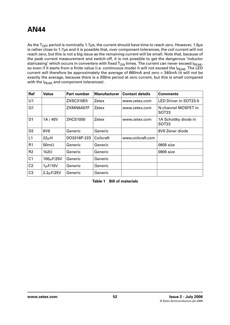
Ref Value Part number Manufacturer Contact details Comments
U1 ZXSC310E5 Zetex www.zetex.com LED Driver in SOT23-5
Q1 ZXMN6A07F Zetex www.zetex.com N-channel MOSFET in SOT23
D1 1A / 40V ZHCS1000 Zetex www.zetex.com 1A Schottky diode in SOT23
D2 6V8 Generic Generic 6V8 Zener diode
L1 22H DO3316P-223 Coilcraft www.coilcraft.com
R1 50m Generic Generic 0805 size
R2 1k2 Generic Generic 0805 size
C1 100F/25V Generic Generic
C2 1F/10V Generic Generic
C3 2.2F/25V Generic Generic
Table 1 Bill of materials
www.zetex.com 52 Issue 2 - July 2006© Zetex Semiconductors plc 2006

AN44
Typical performance graphs for 12V system
Figure 4 Performance graphs for 12V system
By changing the value of R2 from 1k2 to 2k2 the operating input voltage range can be adjustedfrom 30V to 20V, therefore the solution is able to operate from the typical operating voltagesupplies of 12V and 24V for low voltage lighting.
Typical performance graphs for 24V system
Figure 5 Performance graphs for 24V system
Issue 2 - July 2006 53 www.zetex.com© Zetex Semiconductors plc 2006

AN44
Useful formulae for calculations
The input power from the battery during TON (assuming discontinuous operation mode) is VIN *IPEAK/2. The average input current from the battery is therefore this current multiplied by the ratioof TON to the total cycle time:
It can be seen from this how the average battery current will increase at lower VIN as TON becomeslarger compared to the fixed 1.7µs TOFF. This is logical, as the fixed (approximately) LED powerwill require more battery current at lower battery voltage to draw the same power.
The energy which is stored in the inductor equals the energy which is transferred from theinductor to the LED (assuming discontinuous operation) is:
½ * L1 * IPEAK2 [Joules]
Therefore, when the input and the output voltage difference are greater, the LED will have moreenergy which will be transferred from the inductor to the LED rather than be directly obtainedfrom the battery. If the inductor size L1 and peak current IPEAK can be calculated such that thecurrent just reaches zero in 1.7µs, then the power in the LED will not be too dependent on batteryvolts, since the average current in the LED will always be approximately IPEAK/2.
As the battery voltage increases, the TON necessary to reach IPEAK will decrease, but the LEDpower will be substantially constant and it will just draw a battery current ramping from zero toIPEAK during TON. At higher battery voltages, TON will have a lower proportional of the total cycletime, so that the average battery current at higher battery voltage will be less, such that power(and efficiency) is conserved.
The forward voltage which is across the Schottky diode detracts from the efficiency. For example,assuming VF of the LED is 6V and VF of the Schottky is 0.3V, the efficiency loss of energy which istransferred from the inductor is 5%, i.e. the ratio of the Schottky forward drop to the LED forwarddrop. The Schottky is not in circuit during the TON period and therefore does not cause a loss, sothe overall percentage loss will depend on the ratio of the TON and TOFF periods. For low batteryvoltages where TON is a large proportion of the cycle, the Schottky loss will not be significant. TheSchottky loss will also be less significant at higher LED voltages (more LED's in series) as Schottkydrop becomes a lower percentage of the total voltage.
IPEAK2
----------------TON
TON TOFF×---------------------------------×
TONIPEAK L1×
VBATT VLED–( )---------------------------------------------=
www.zetex.com 54 Issue 2 - July 2006© Zetex Semiconductors plc 2006
AN47
Getting more out of the ZXLD1350 - dimming techniquesRay Liu, Systems Engineer, Zetex Semiconductors
Introduction
The ZXLD1350 has a versatile adjust pin that can be used in many ways to adjust the brightnessof the LED by controlling the current in the LED. This application note deals with some the waysin which dimming the LED can be achieved and discusses the merits of the techniques. Thesedimming methods discussed include PWM dimming both with a low and high frequency signals,DC voltage control and resistive dimming.
Low frequency dimming
Low frequency dimming is preferred for LED dimming since the LED instantaneous drivingcurrent is constant. The color temperature of the LED is preserved at all dimming levels. Anotheradvantage of low frequency dimming is that the dimming level can down to 1%. Hence result indimming range of 100:1.
Choice of frequency
To avoid visible flicker the PWM signal must be greater than 100Hz. If you choose too high afrequency the internal low pass filter will start to integrate the PWM signal and produce a nonlinear response. Also the soft start function of the ADJ pin will cause a delay on the rising a fallingedge of the PWM signal. This can give a non-linearity in the LED current which will have a greateraffect as frequency increases.
An upper limit of 1kHz is suggested. The effect of audible noise in the inductor may need to beconsidered. This may happen in some inductors with loose windings and will be more noticeableat PWM frequencies of 1kHz than 100Hz.
If the PWM frequency is less than approximately 500Hz, the device will be gated 'on' and 'off' andthe output will be discontinuous, with an average value of output current given by:
[for 0<DWPM<1]
High frequency dimming
High frequency dimming is preferred if system required low radiated emission and in/outputripple. But dimming range is reduced to 5:1. The ZXLD1350 has an internal low pass filter whichintegrates the high frequency PWM signal to produce a DC dimming control.
IOUT
0.1 DPWM
RS
--------------------------≈
PWMGND
ZXLD1350ADJ
GND
Issue 1 - August 2006 55 www.zetex.com© Zetex Semiconductors plc 2006
AN47
If the PWM frequency is higher than approximately 10kHz and the duty cycle above the specifiedminimum value, the device will remain active and the output will be continuous, with a nominaloutput current given by:
[for 0.16< DPWM <1]
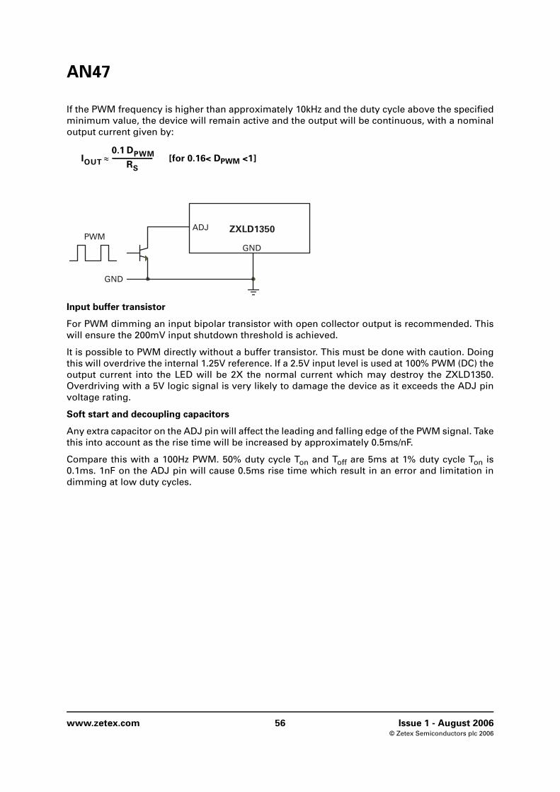
Input buffer transistor
For PWM dimming an input bipolar transistor with open collector output is recommended. Thiswill ensure the 200mV input shutdown threshold is achieved.
It is possible to PWM directly without a buffer transistor. This must be done with caution. Doingthis will overdrive the internal 1.25V reference. If a 2.5V input level is used at 100% PWM (DC) theoutput current into the LED will be 2X the normal current which may destroy the ZXLD1350.Overdriving with a 5V logic signal is very likely to damage the device as it exceeds the ADJ pinvoltage rating.
Soft start and decoupling capacitors
Any extra capacitor on the ADJ pin will affect the leading and falling edge of the PWM signal. Takethis into account as the rise time will be increased by approximately 0.5ms/nF.
Compare this with a 100Hz PWM. 50% duty cycle Ton and Toff are 5ms at 1% duty cycle Ton is0.1ms. 1nF on the ADJ pin will cause 0.5ms rise time which result in an error and limitation indimming at low duty cycles.
IOUT
0.1 DPWM
RS
--------------------------≈
PWMGND
ZXLD1350ADJ
GND
www.zetex.com 56 Issue 1 - August 2006© Zetex Semiconductors plc 2006

AN47
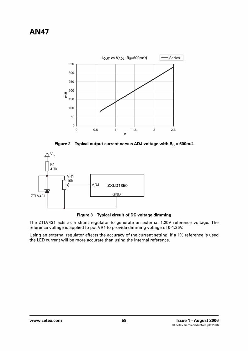
DC voltage dimming
The ADJ pin can be overdriven by an external DC voltage (VADJ), as shown, in order to overridethe internal voltage reference and adjust the output current to a value above or below the nominalvalue.
The nominal output current is then given by:
[for 0.3< VADJ <2.5V]
Note that 100% brightness setting corresponds to VADJ = VREF.
If VIN is 2.5V max the RSENSE should be increased by 2X RS. This will slightly decrease theefficiency by 1 to 2% .
The input impedance of the ADJ pin is 200k ±20%. This may be factor if the DC voltage with arelatively high output resistance.
Figure 1 Typical output current versus ADJ voltage with RS = 300m
GND
ZXLD1350ADJ
GND
+
DC
IOUT
0.08 V× ADJ
RS
--------------------------------≈
IOUT vs VADJ (RS=300m)
0
50
100
150
200
250
300
350
0 0.25 0.5 0.75 1 1.25V
mA
Series1
Issue 1 - August 2006 57 www.zetex.com© Zetex Semiconductors plc 2006
AN47
Figure 2 Typical output current versus ADJ voltage with RS = 600m
Figure 3 Typical circuit of DC voltage dimming
The ZTLV431 acts as a shunt regulator to generate an external 1.25V reference voltage. Thereference voltage is applied to pot VR1 to provide dimming voltage of 0-1.25V.
Using an external regulator affects the accuracy of the current setting. If a 1% reference is usedthe LED current will be more accurate than using the internal reference.
IOUT vs VADJ (RS=600m)
0
50
100
150
200
250
300
350
0 0.5 1 1.5 2 2.5V
mA
Series1
GND
ZXLD1350ADJ
ZTLV431
VR110k
R14.7k
VIN
www.zetex.com 58 Issue 1 - August 2006© Zetex Semiconductors plc 2006
AN47
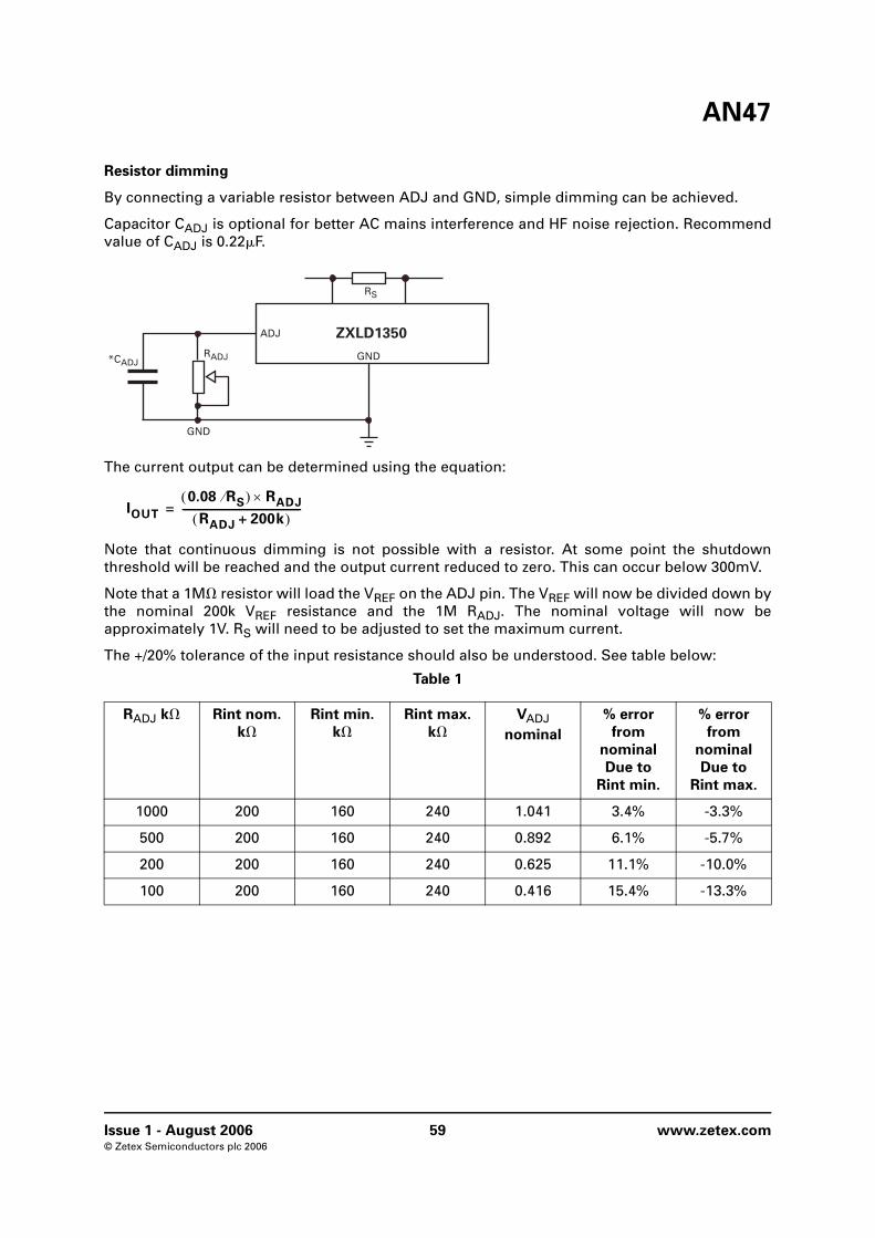
Resistor dimming
By connecting a variable resistor between ADJ and GND, simple dimming can be achieved.
Capacitor CADJ is optional for better AC mains interference and HF noise rejection. Recommendvalue of CADJ is 0.22F.
The current output can be determined using the equation:
Note that continuous dimming is not possible with a resistor. At some point the shutdownthreshold will be reached and the output current reduced to zero. This can occur below 300mV.
Note that a 1M resistor will load the VREF on the ADJ pin. The VREF will now be divided down bythe nominal 200k VREF resistance and the 1M RADJ. The nominal voltage will now beapproximately 1V. RS will need to be adjusted to set the maximum current.
The +/20% tolerance of the input resistance should also be understood. See table below:
Table 1
RADJ k Rint nom.
kRint min.
kRint max.
kVADJ
nominal
% error
from
nominal
Due to
Rint min.
% error
from
nominal
Due to
Rint max.
1000 200 160 240 1.041 3.4% -3.3%
500 200 160 240 0.892 6.1% -5.7%
200 200 160 240 0.625 11.1% -10.0%
100 200 160 240 0.416 15.4% -13.3%
GND
ZXLD1350ADJ
GND
RADJ
RS
*CADJ
IOUT
0.08 RS⁄( ) RADJ×RADJ 200k+( )
------------------------------------------------=
Issue 1 - August 2006 59 www.zetex.com© Zetex Semiconductors plc 2006
AN47
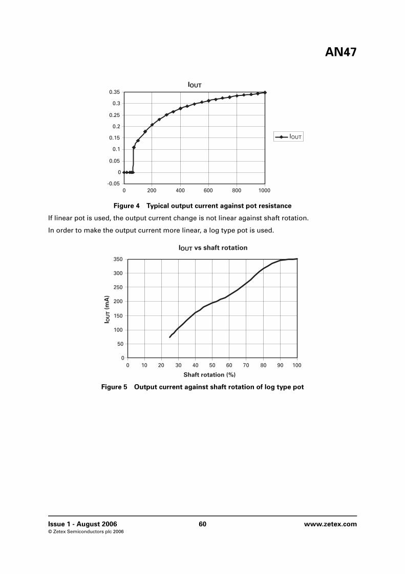
Figure 4 Typical output current against pot resistance
If linear pot is used, the output current change is not linear against shaft rotation.
In order to make the output current more linear, a log type pot is used.
Figure 5 Output current against shaft rotation of log type pot
IOUT
-0.05
0
0.05
0.1
0.15
0.2
0.25
0.3
0.35
0 200 400 600 800 1000
IOUT
IOUT vs shaft rotation
0
50
100
150
200
250
300
350
0 10 20 30 40 50 60 70 80 90 100
Shaft rotation (%)
I OU
T (
mA
)
Issue 1 - August 2006 60 www.zetex.com© Zetex Semiconductors plc 2006
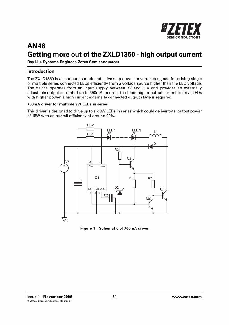
AN48
Getting more out of the ZXLD1350 - high output currentRay Liu, Systems Engineer, Zetex Semiconductors
Introduction
The ZXLD1350 is a continuous mode inductive step-down converter, designed for driving singleor multiple series connected LEDs efficiently from a voltage source higher than the LED voltage.The device operates from an input supply between 7V and 30V and provides an externallyadjustable output current of up to 350mA. In order to obtain higher output current to drive LEDswith higher power, a high current externally connected output stage is required.
700mA driver for multiple 3W LEDs in series
This driver is designed to drive up to six 3W LEDs in series which could deliver total output powerof 15W with an overall efficiency of around 90%.
Figure 1 Schematic of 700mA driver
Q1
Q2
Q3
Q1
VIN
LX GND ADJ
ISENSE
46
1 2 3
LED1 LEDN
D1
C1
V6
0
+
-
C2
L1
R1
RS2
RS1
R2
R3
D2
Issue 1 - November 2006 61 www.zetex.com© Zetex Semiconductors plc 2006
AN48
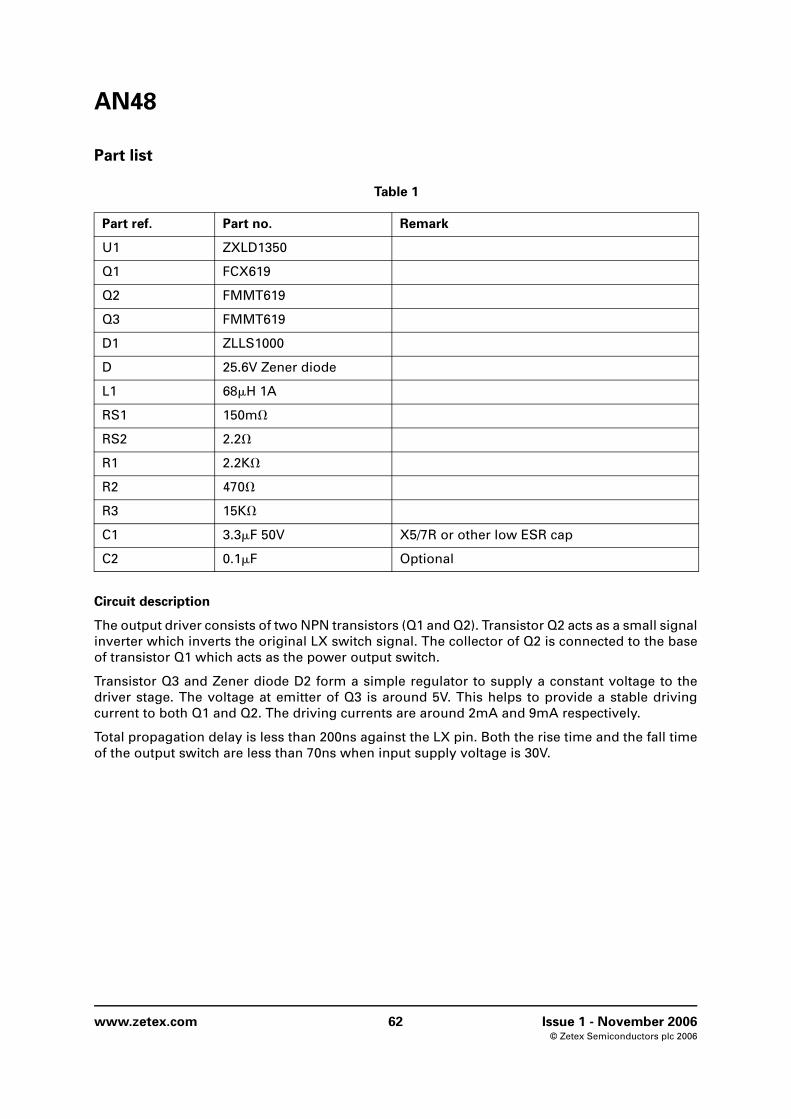
Part list
Circuit description
The output driver consists of two NPN transistors (Q1 and Q2). Transistor Q2 acts as a small signalinverter which inverts the original LX switch signal. The collector of Q2 is connected to the baseof transistor Q1 which acts as the power output switch.
Transistor Q3 and Zener diode D2 form a simple regulator to supply a constant voltage to thedriver stage. The voltage at emitter of Q3 is around 5V. This helps to provide a stable drivingcurrent to both Q1 and Q2. The driving currents are around 2mA and 9mA respectively.
Total propagation delay is less than 200ns against the LX pin. Both the rise time and the fall timeof the output switch are less than 70ns when input supply voltage is 30V.
Table 1
Part ref. Part no. Remark
U1 ZXLD1350
Q1 FCX619
Q2 FMMT619
Q3 FMMT619
D1 ZLLS1000
D 25.6V Zener diode
L1 68H 1A
RS1 150m
RS2 2.2
R1 2.2K
R2 470
R3 15K
C1 3.3F 50V X5/7R or other low ESR cap
C2 0.1F Optional
www.zetex.com 62 Issue 1 - November 2006© Zetex Semiconductors plc 2006
AN48
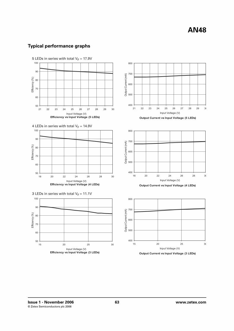
Typical performance graphs
Efficiency vs Input Voltage (5 LEDs)
50
60
70
80
90
100
21 22 23 24 25 26 27 28 29 30
Input Voltage (V)
Effic
ienc
y (%
)
Efficiency vs Input Voltage (4 LEDs)
50
60
70
80
90
100
18 20 22 24 26 28 30
Input Voltage (V)
Effic
ienc
y (%
)
4 LEDs in series with total VF = 14.9V
5 LEDs in series with total VF = 17.9V
Efficiency vs Input Voltage (3 LEDs)
50
60
70
80
90
100
15 20 25 30
Input Voltage (V)
Effic
ienc
y (%
)
Output Current vs Input Voltage (3 LEDs)
400
500
600
700
800
15 20 25 30
Input Voltage (V)
Out
put C
urre
nt (m
A)
Output Current vs Input Voltage (4 LEDs)
400
500
600
700
800
18 20 22 24 26 28 30
Input Voltage (V)
Out
put C
urre
nt (m
A)
Output Current vs Input Voltage (5 LEDs)
400
500
600
700
800
21 22 23 24 25 26 27 28 29 30
Input Voltage (V)
Out
put C
urre
nt (m
A)
3 LEDs in series with total VF = 11.1V
Issue 1 - November 2006 63 www.zetex.com© Zetex Semiconductors plc 2006
AN48
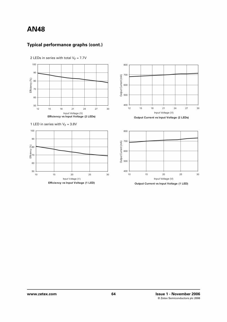
Typical performance graphs (cont.)
Efficiency vs Input Voltage (2 LEDs)
50
60
70
80
90
100
12 15 18 21 24 27 30
Input Voltage (V)
Effic
ienc
y (%
)
Output Current vs Input Voltage (2 LEDs)
400
500
600
700
800
12 15 18 21 24 27 30
Input Voltage (V)
Out
put C
urre
nt (m
A)
Efficiency vs Input Voltage (1 LED)
50
60
70
80
90
100
10 15 20 25 30
Input Voltage (V)
Effic
ienc
y (%
)
Output Current vs Input Voltage (1 LED)
400
500
600
700
800
10 15 20 25 30
Input Voltage (V)
Out
put C
urre
nt (m
A)1 LED in series with VF = 3.8V
2 LEDs in series with total VF = 7.7V
www.zetex.com 64 Issue 1 - November 2006© Zetex Semiconductors plc 2006

AN48
A driver for supply voltage up to 16V
This driver is a simplified version to the 700mA driver described above. The driver is designed todrive up to 3 Luxeon® K2 LEDs in series which could deliver a total output power of 10W with amaximum input supply voltage of 16V.
Figure 2 Schematic of 1A driver
Part List
Table 2
Part ref. Part no. Remark
U1 ZXLD1350
Q1 ZXTN25020DFH
Q2 ZXTN25020DFH
D1 ZLLS2000
L14 7H 1.5A
RS 100m
R1 4.7K
R2 1.5K
C1 4.7F 25V X5/7R or other low ESR cap
C2 0.1F Optional
Q1
Q2
Q1
VIN
LX GND ADJ
ISENSE
46
1 2 3
LED1 LEDN
D1
C1
V6
0
+
-
C2
L1
R1
RS1
R2
Issue 1 - November 2006 65 www.zetex.com© Zetex Semiconductors plc 2006

AN48
Circuit description
This circuit is similar to the 700mA driver described above. The output driver consists of two NPNtransistors (Q1 and Q2). Transistor Q2 acts as a small signal inverter which inverts the original LXswitch signal. The collector of Q2 is connected to the base of transistor Q1 which act as the poweroutput switch.
Unlike the 700mA driver, the driving current to both Q1 and Q2 varies with the input supplyvoltage. Hence, the maximum input supply voltage is limited to 16V. The driving current to Q1 isbetween 5mA and 10mA with input supply voltage between 8V and 16V. Lowering the maximumsupply voltage to 16V enables us to use a lower voltage BJT with better switching performance.
Total propagation delay is less than 200ns against the LX pin. Both the rise time and the fall timeof the output switch are less than 60ns when input supply voltage is 16V.
www.zetex.com 66 Issue 1 - November 2006© Zetex Semiconductors plc 2006
AN48
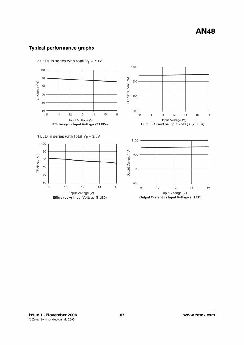
Typical performance graphs
Efficiency vs Input Voltage (2 LEDs)
50
60
70
80
90
100
10 11 12 13 14 15 16
Input Voltage (V)
Effic
ienc
y (%
)
Output Current vs Input Voltage (2 LEDs)
500
700
900
1100
10 11 12 13 14 15 16
Input Voltage (V)
Out
put C
urre
nt (m
A)
Efficiency vs Input Voltage (1 LED)
50
60
70
80
90
100
8 10 12 14 16
Input Voltage (V)
Effic
ienc
y (%
)
Output Current vs Input Voltage (1 LED)
500
700
900
1100
8 10 12 14 16
Input Voltage (V)
Out
put C
urre
nt (m
A)
2 LEDs in series with total VF = 7.1V
1 LED in series with total VF = 3.5V
Issue 1 - November 2006 67 www.zetex.com© Zetex Semiconductors plc 2006

Intentionally left blank
Issue 6 - November 2006 68 www.zetex.com© Zetex Semiconductors plc 2006

Intentionally left blank
Issue 6 - November 2006 69 www.zetex.com© Zetex Semiconductors plc 2006

Intentionally left blank
Issue 6 - November 2006 70 www.zetex.com© Zetex Semiconductors plc 2006

Intentionally left blank
Issue 6 - November 2006 71 www.zetex.com© Zetex Semiconductors plc 2006

www.zetex.com 72 Issue 6 - November 2006© Zetex Semiconductors plc 2006
Definitions
Product change
Zetex Semiconductors reserves the right to alter, without notice, specifications, design, price or conditions of supply of any product orservice. Customers are solely responsible for obtaining the latest relevant information before placing orders.Applications disclaimer
The circuits in this design/application note are offered as design ideas. It is the responsibility of the user to ensure that the circuit is fit forthe user’s application and meets with the user’s requirements. No representation or warranty is given and no liability whatsoever isassumed by Zetex with respect to the accuracy or use of such information, or infringement of patents or other intellectual property rightsarising from such use or otherwise. Zetex does not assume any legal responsibility or will not be held legally liable (whether in contract,tort (including negligence), breach of statutory duty, restriction or otherwise) for any damages, loss of profit, business, contract,opportunity or consequential loss in the use of these circuit applications, under any circumstances.Life support
Zetex products are specifically not authorized for use as critical components in life support devices or systems without the express writtenapproval of the Chief Executive Officer of Zetex Semiconductors plc. As used herein:A. Life support devices or systems are devices or systems which:
1. are intended to implant into the body or
2. support or sustain life and whose failure to perform when properly used in accordance with instructions for use provided in thelabelling can be reasonably expected to result in significant injury to the user.
B. A critical component is any component in a life support device or system whose failure to perform can be reasonably expected to cause the failure of the life support device or to affect its safety or effectiveness.
Reproduction
The product specifications contained in this publication are issued to provide outline information only which (unless agreed by thecompany in writing) may not be used, applied or reproduced for any purpose or form part of any order or contract or be regarded as arepresentation relating to the products or services concerned. Terms and Conditions
All products are sold subjects to Zetex’ terms and conditions of sale, and this disclaimer (save in the event of a conflict between the twowhen the terms of the contract shall prevail) according to region, supplied at the time of order acknowledgement.For the latest information on technology, delivery terms and conditions and prices, please contact your nearest Zetex sales office.Quality of product
Zetex is an ISO 9001 and TS16949 certified semiconductor manufacturer.To ensure quality of service and products we strongly advise the purchase of parts directly from Zetex Semiconductors or one of ourregionally authorized distributors. For a complete listing of authorized distributors please visit: www.zetex.com/salesnetwork
Zetex Semiconductors does not warrant or accept any liability whatsoever in respect of any parts purchased through unauthorized sales channels.ESD (Electrostatic discharge)
Semiconductor devices are susceptible to damage by ESD. Suitable precautions should be taken when handling and transporting devices.The possible damage to devices depends on the circumstances of the handling and transporting, and the nature of the device. The extentof damage can vary from immediate functional or parametric malfunction to degradation of function or performance in use over time.Devices suspected of being affected should be replaced.Green compliance
Zetex Semiconductors is committed to environmental excellence in all aspects of its operations which includes meeting or exceedingregulatory requirements with respect to the use of hazardous substances. Numerous successful programs have been implemented toreduce the use of hazardous substances and/or emissions. All Zetex components are compliant with the RoHS directive, and through this it is supporting its customers in their compliance withWEEE and ELV directives.Product status key:
“Preview” Future device intended for production at some point. Samples may be available“Active” Product status recommended for new designs“Last time buy (LTB)” Device will be discontinued and last time buy period and delivery is in effect“Not recommended for new designs” Device is still in production to support existing designs and production“Obsolete” Production has been discontinuedDatasheet status key:
“Draft version” This term denotes a very early datasheet version and contains highly provisional information, whichmay change in any manner without notice.
“Provisional version” This term denotes a pre-release datasheet. It provides a clear indication of anticipated performance.However, changes to the test conditions and specifications may occur, at any time and without notice.
“Issue” This term denotes an issued datasheet containing finalized specifications. However, changes tospecifications may occur, at any time and without notice.
Zetex sales offices
Europe
Zetex GmbHKustermann-parkBalanstraße 59D-81541 MünchenGermanyTelefon: (49) 89 45 49 49 0Fax: (49) 89 45 49 49 [email protected]
Americas
Zetex Inc700 Veterans Memorial HighwayHauppauge, NY 11788USA
Telephone: (1) 631 360 2222Fax: (1) 631 360 [email protected]
Asia Pacific
Zetex (Asia Ltd)3701-04 Metroplaza Tower 1Hing Fong Road, Kwai FongHong Kong
Telephone: (852) 26100 611Fax: (852) 24250 [email protected]
Corporate Headquarters
Zetex Semiconductors plcZetex Technology Park, ChaddertonOldham, OL9 9LLUnited Kingdom
Telephone: (44) 161 622 4444Fax: (44) 161 622 [email protected]
© 2006 Published by Zetex Semiconductors plc
SCLIGHTDNV3