dn05073 - universal ac input, 5.3 v 2 a output, 10.6 w charger
TRANSCRIPT

© Semiconductor Components Industries, LLC, 2016
August, 2016 − Rev. 11 Publication Order Number:
DN05073/D
DN05073/D
Universal AC Input, 5.3 V 2 A Output, 10.6 W ChargerUsing NCP1360
Table 1. DEVICE DETAILS
Device Application Input Voltage Output Power Topology I/O Isolation
NCP1360BBCCNCP1360BCCC
Mobile, Tablet, Charger, Adapter
90 to 264 Vac 10.6 W Quasi ResonantFlyback
Yes
Item Output Specification Test Condition
Rated Input Voltage 100 ~ 240 Vac −
Input Voltage Range 90 ~ 264 Vac −
Input Frequency Range 47 ~ 63 Hz −
Inrush Current < 30 A 264 Vac and 2 A Load
Average Efficiency > 82% Measured at Board End
Average Efficiency at Cable End > 78% Measured at Cable End
Standby Power < 50 mW & 75 mW 90 ~ 264 Vac
Output Voltage 5 ~ 5.5 V, 5.3 V at 2 A 90 ~ 264 Vac and 0 ~ 2 A
Output Current 2 A 90 ~ 264 Vac
Rated Output Power > 10.6 W 90 ~ 264 Vac
Ripple and Noise < 120 mV 90 ~ 264 Vac, 1 �F + 0.1 �F CAP@E-load
Rise Time < 30 ms At No/Full Load, 115 Vac & 230 Vac
Start-up Time < 1 .5 s 90 ~ 264 Vac and 0 ~ 2 A
Over Shoot < 6.4 V At 1 m USB Cable End
Transient Response 4.5 ~ 5.5 V 0.1−1.9 A, 0.25 A/�s, 10 ms Cycle
Circuit DescriptionThis design note describes a 10.6 W, universal AC input,
isolated Quasi-Resonant flyback converter for smart phone,tablet charger and smart socket power supply etc.
The featured power supply is a primary side constantvoltage and current regulation utilizing ON Semiconductor’snew NCP1360 current mode controller which is in TSOP−6package. This design note provides the complete circuitschematic details, layout, test data and BOM for 5.3 V, 2 Apower supply.
Both NCP1360BBCC and NCP1360BCCC are all testedin this design, it has almost same performance exceptstandby power and dynamic response.
1. Input Circuit:Rectifier, filter and EMC circuit formed by D1,C1, C1, L1, NTC is 2.5 � negative temperaturecoefficient resistor to provide inrush protection,FR1 provides short-circuit protection when largeAC input current occurs.
2. NCP1360 Control Circuit:R8 and R9 consists of voltage simple network toset output voltage, C12 is a delayed capacitor todelay switching on to valley.R12 and R13 is a current sensing resistor to decidehow much current can be set, R10 and CS pinparasitic capacitor consists of a filter to filtercurrent spike. R19, C11 and C9 consist of a type IIcompensation network to provide voltage feedback
www.onsemi.com
DESIGN NOTE

DN05073/D
www.onsemi.com2
control loop compensation.R5 and R11 is start-up resistor, two 7.5 M� areused in series to reduce power loss, R4, D6 and C4consist of VCC supply circuit, R4 can adjust VCCvoltage and also prevent D6 from an inrushcurrent. An RCD−R clamp consisting of D5, R3,R6, and C7 limits drain voltage spikes caused byleakage inductance, resistor R6 has a relativelylarge value to prevent any excessive ringing on thedrain voltage waveform and R3 can limit thereverse recovery current through D5.
3. Output Rectification and Filter:The transformer (T1) secondary is rectified by D2,a Schottky barrier-type diode (chosen for higherefficiency), and filtered by C3, C5 and C8. In thisapplication, C3 and C5 have sufficiently low ESRcharacteristics to allow meeting the output voltageripple requirement without adding an LC postfilter. C6 and R7 are snubber network of D2 toeliminate excessive ringing on secondary voltagewaveform. R14 is a dummy load to prevent outputvoltage rising at no load.
Key Features• Primary Side Regulation (PSR) CC/CV Control
• Quasi-Resonant Current Mode Control with ValleySwitching
• Valley Lockout Avoids Audible Noise at ValleyJumping Operation
• Built in 4 ms Soft Start
• 110 kHz Maximum Clamp Frequency Operation
• Adjustable Voltage Control Loop Compensation
• 300 mV Cable Drop Compensation
• Wide Operation VCC Range (Up to 30 V)
• Cycle by Cycle Current Limit
• Support External 1500 �F Capacitive Load Start-up
• Built in VCC OVP (Typical 26 V)
• Built in Output UVP in CC Mode (3 V ±6.7%)
• Output OCP, SCP, OVP and Controller OTP Function
• CS Pin Open and Short Protection
• Vs Pin Open and Short Protection
• Meet COC V5 Tier 2
• 100 pF Y Capacitor
• “Travel Adapter” (TA) Form Factor
• Size: 47 × 34 × 15 mm
PCB Layout
Figure 1. PCB Layout
Demoboard Photo
Figure 2. Demoboard Photo

DN05073/D
www.onsemi.com3
Circuit Schematic
Figure 3. Circuit Schematic
L122
0 �H
FR
11.
6 A
, 250
Vac
NT
C2.
5 �
L N
AC
AC
+ −
++
C1
10 �
F,40
0 V
C2
10 �
F, 4
00 V
R5
7.5
M�
R11
7.5
M�
R3
150 �
R6
330
k�
C7
390
pF,
630
V
D6
BA
S20
HT
1GR4
4.7 �
D1
1 A
, 600
V
R15
47 � D4
BA
S20
HT
1G
R8
100
k� R9
30.9
k�
R2
NA
R19
82 k�
R10
1 k�
C11
33 n
F
C9
100
pFC
1210
pF
R12
1.6 �
R13
1.8 �
C4
1 �F,
35 V
C11
100
pF, Y
1
U1
NC
P13
60
16
25
34
VS
CO
MP
CS
VC
C
GN
DD
RV
Q1
SW
6N70
D2
MB
R20
45M
FS
/F
ER
D30
S50 R
720
�
C6
1000
pF
T1
1
2
45
6 7
R14
1.6
k� @
600
Hz
800 �
@ 1
.2 k
Hz
J1−
1
J1−
2
J1−
3
J1−
4R
181
M�
C5
470 �F,
6.3
V
++ C
347
0 �F,
6.3
V
C8
0.1 �F
Inpu
t Vol
tage
: 90
Vac
to 2
64 V
acO
utpu
t: 5.
3 V
dc, 2
A
T1
Cor
e: E
I16/
12/8
Bob
bin:
10-
pin
TH
Typ
eLp
: 1.2
5 m
HN
p:N
s:N
a =
75T
:5T:
11T
D5
DF
LR16
00
G
D S

DN05073/D
www.onsemi.com4
Standby Power for NCP1360BBCC at No Load
Figure 4. Standby Power for NCP1360BBCC at No Load
Standby Power for NCP1360BCCC at No Load
Figure 5. Standby Power for NCP1360BCCC at No Load

DN05073/D
www.onsemi.com5
Average Efficiency between 25%, 50%, 75% and 100% Load
Figure 6. Average Efficiency between 25%, 50%, 75% and 100% Load
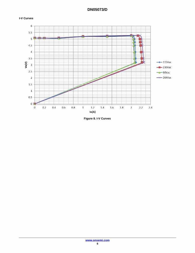
Efficiency vs. Load Curves
Figure 7. Efficiency vs. Load Curves

DN05073/D
www.onsemi.com7
OUTPUT RIPPLE VOLTAGE(Test Condition: Tested at E-load with 1 m Cable, 1 �F E-CAP and 0.1 �F Ceramic in Parallel)
Figure 9. 90 Vac and 2 A Load Figure 10. 115 Vac and 2 A Load
Figure 11. 230 Vac and 0.5 A Load Figure 12. 264 Vac and 0.5 A Load
TRANSIENT RESPONSE FOR NCP1360BBCC
Figure 13. Test Conditions: 0.2−1.8 A, 250 mA/�s, 10 ms Cycle, 115 Vac
Figure 14. Test Conditions: 0.1−1.9 A, 250 mA/�s, 10 ms Cycle, 115 Vac

DN05073/D
www.onsemi.com8
TRANSIENT RESPONSE FOR NCP1360BCCC
Figure 15. Test Conditions: 50 mA−2 A, 250 mA/�s, 20 ms Cycle, 115 Vac
Figure 16. Test Conditions: 50 mA−2 A, 250 mA/�s, 10 ms Cycle, 115 Vac
Figure 17. Test Conditions: 0.2−1.8 A, 250 mA/�s, 10 ms Cycle, 115 Vac
Figure 18. Test Conditions: 0.1−1.9 A, 250 mA/�s, 10 ms Cycle, 115 Vac
OVP AND SCP
Figure 19. Test Conditions: 264 Vac, No Dummy Load Figure 20. Test Conditions: SC at Board End

DN05073/D
www.onsemi.com9
START-UP TIME
Figure 21. 90 Vac and 2 A CC Load Figure 22. 230 Vac and 2 A CC Load
OUTPUT VOLTAGE RISE TIME
Figure 23. 115 Vac and 2 A CC Load Figure 24. 230 Vac and 2 A CC Load
OUTPUT VOLTAGE OVERSHOOT
Figure 25. 115 Vac and No Load Figure 26. 115 Vac and 2 A CC Load

DN05073/D
www.onsemi.com10
EXTERNAL 1500 �F CAPACITIVE LOAD START-UP
Figure 27. Test Conditions:Ext. 1500 �F capacitor, 2 A CC Load with 1 V Von Voltage Set, 90 Vac
MOSFET DRAIN VOLTAGE
Figure 28. Startup at 264 Vac and 2 A CC Load Figure 29. Working at 264 Vac and 2 A CC Load
INRUSH CURRENT
Figure 30. 264 Vac and 2 A CC Load

DN05073/D
www.onsemi.com11
SECONDARY DIODE REVERSE VOLTAGE
Figure 31. 264 Vac and 2 A CC Load
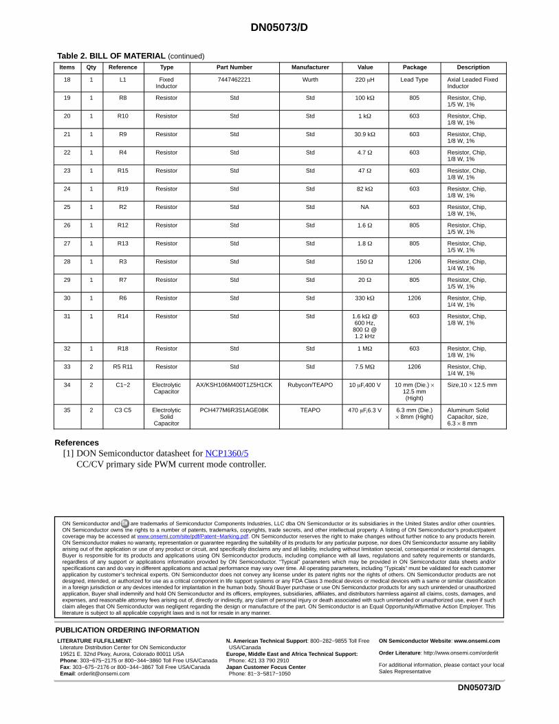
Bill of Material
Table 2. BILL OF MATERIAL Items Qty Reference Type Part Number Manufacturer Value Package Description
1 1 C8 Ceramic Std Std 0.1 �F, 50 V 603 Capacitor,Ceramic, 10%
2 1 C6 Ceramic Std Std 1000 pF,50 V
603 Capacitor,Ceramic, 10%
3 1 C9 Ceramic Std Std 100 pF, 50 V 603 Capacitor,Ceramic, Chip,10%
4 1 C10 CeramicCapacitor
CS65−B2GA101KYNKA TDK 100 pF, Y1 Lead Type HV CeramicCapacitor, SafetyStandardApproved, 10%
5 1 C12 Ceramic Std Std 10 pF, 50 V 603 Capacitor,Ceramic, Chip,10%
6 1 C4 Ceramic C2012X7R1E105K TDK 1 �F, 35 V 805 Capacitor,Ceramic, Chip,10%
7 1 C11 Ceramic Std Std 33 nF, 50 V 603 Capacitor,Ceramic, Chip,10%
8 1 C7 CeramicCapacitor
C3216C0G2J391J TDK 390 pF,630 V
1206 Capacitor,Ceramic, Chip, 5%
9 1 D1 BridgeRectifier
LMB6S FSC/Others 1 A, 600 V Micro-DIP Bridge Rectifier,600 V, 1 A
10 1 D2 SchottkyRectifier
MBR2045MFS/FERD30S50 ON/ST 20 A, 45 V SO8FL Schottky Rectifier,20 A, 4 5V/ 30 A, 50 V
11 1 D5 StandardRectifier
DFLR1600 Diodes 1 A, 600 V POWERDI123 Standard Rectifier,1 A, 600 V
12 2 D4, D6 SwitchingDiode
BAS20HT1G ON Semiconductor 0.2 A, 200 V SOD323 Switching Diode,SMD
13 1 T1 Transformer EI16/12/8 Customized Transformer TH Type Core: EI16/12/8,CustomizedBobbin, 10-pin
14 1 FR1 Micro Fuse 20T−016H HollyFUSE 1.6 A,250 Vac
Radial Lead Micro Fuse,1.6 A/250 Vac,Radial Lead
15 1 U1 PSRController
NCP1360BBCC/BCCC ON Semiconductor TSOP−6 PSR Controllerwithout HV Start-upSource, TSOP−6
16 1 Q1 NMOSFET SW6N70 SAMWIN 6 A, 700 V IPAK NMOS, 6 A, 700 V,IPAK
17 1 NTC NTC SPNL07D2R5MBI Sunlord 2.5 � Lead Type NTC, 2.5 �, 3 A
DN05073/D
www.onsemi.com12
Table 2. BILL OF MATERIAL (continued)
Items DescriptionPackageValueManufacturerPart NumberTypeReferenceQty
18 1 L1 FixedInductor
7447462221 Wurth 220 �H Lead Type Axial Leaded FixedInductor
19 1 R8 Resistor Std Std 100 k� 805 Resistor, Chip,1/5 W, 1%
20 1 R10 Resistor Std Std 1 k� 603 Resistor, Chip,1/8 W, 1%
21 1 R9 Resistor Std Std 30.9 k� 603 Resistor, Chip,1/8 W, 1%
22 1 R4 Resistor Std Std 4.7 � 603 Resistor, Chip,1/8 W, 1%
23 1 R15 Resistor Std Std 47 � 603 Resistor, Chip,1/8 W, 1%
24 1 R19 Resistor Std Std 82 k� 603 Resistor, Chip,1/8 W, 1%
25 1 R2 Resistor Std Std NA 603 Resistor, Chip,1/8 W, 1%,
26 1 R12 Resistor Std Std 1.6 � 805 Resistor, Chip,1/5 W, 1%
27 1 R13 Resistor Std Std 1.8 � 805 Resistor, Chip,1/5 W, 1%
28 1 R3 Resistor Std Std 150 � 1206 Resistor, Chip,1/4 W, 1%
29 1 R7 Resistor Std Std 20 � 805 Resistor, Chip,1/5 W, 1%
30 1 R6 Resistor Std Std 330 k� 1206 Resistor, Chip,1/4 W, 1%
31 1 R14 Resistor Std Std 1.6 k� @600 Hz,
800 � @1.2 kHz
603 Resistor, Chip,1/8 W, 1%
32 1 R18 Resistor Std Std 1 M� 603 Resistor, Chip,1/8 W, 1%
33 2 R5 R11 Resistor Std Std 7.5 M� 1206 Resistor, Chip,1/4 W, 1%
34 2 C1−2 ElectrolyticCapacitor
AX/KSH106M400T1Z5H1CK Rubycon/TEAPO 10 �F,400 V 10 mm (Die.) ×12.5 mm(Hight)
Size,10 × 12.5 mm
35 2 C3 C5 ElectrolyticSolid
Capacitor
PCH477M6R3S1AGE08K TEAPO 470 �F,6.3 V 6.3 mm (Die.)× 8mm (Hight)
Aluminum SolidCapacitor, size,6.3 × 8 mm
References[1] DON Semiconductor datasheet for NCP1360/5
CC/CV primary side PWM current mode controller.
ON Semiconductor and are trademarks of Semiconductor Components Industries, LLC dba ON Semiconductor or its subsidiaries in the United States and/or other countries.ON Semiconductor owns the rights to a number of patents, trademarks, copyrights, trade secrets, and other intellectual property. A listing of ON Semiconductor’s product/patentcoverage may be accessed at www.onsemi.com/site/pdf/Patent−Marking.pdf. ON Semiconductor reserves the right to make changes without further notice to any products herein.ON Semiconductor makes no warranty, representation or guarantee regarding the suitability of its products for any particular purpose, nor does ON Semiconductor assume any liabilityarising out of the application or use of any product or circuit, and specifically disclaims any and all liability, including without limitation special, consequential or incidental damages.Buyer is responsible for its products and applications using ON Semiconductor products, including compliance with all laws, regulations and safety requirements or standards,regardless of any support or applications information provided by ON Semiconductor. “Typical” parameters which may be provided in ON Semiconductor data sheets and/orspecifications can and do vary in different applications and actual performance may vary over time. All operating parameters, including “Typicals” must be validated for each customerapplication by customer’s technical experts. ON Semiconductor does not convey any license under its patent rights nor the rights of others. ON Semiconductor products are notdesigned, intended, or authorized for use as a critical component in life support systems or any FDA Class 3 medical devices or medical devices with a same or similar classificationin a foreign jurisdiction or any devices intended for implantation in the human body. Should Buyer purchase or use ON Semiconductor products for any such unintended or unauthorizedapplication, Buyer shall indemnify and hold ON Semiconductor and its officers, employees, subsidiaries, affiliates, and distributors harmless against all claims, costs, damages, andexpenses, and reasonable attorney fees arising out of, directly or indirectly, any claim of personal injury or death associated with such unintended or unauthorized use, even if suchclaim alleges that ON Semiconductor was negligent regarding the design or manufacture of the part. ON Semiconductor is an Equal Opportunity/Affirmative Action Employer. Thisliterature is subject to all applicable copyright laws and is not for resale in any manner.
PUBLICATION ORDERING INFORMATIONN. American Technical Support: 800−282−9855 Toll FreeUSA/Canada
Europe, Middle East and Africa Technical Support:Phone: 421 33 790 2910
Japan Customer Focus CenterPhone: 81−3−5817−1050
DN05073/D
LITERATURE FULFILLMENT:Literature Distribution Center for ON Semiconductor19521 E. 32nd Pkwy, Aurora, Colorado 80011 USAPhone: 303−675−2175 or 800−344−3860 Toll Free USA/CanadaFax: 303−675−2176 or 800−344−3867 Toll Free USA/CanadaEmail: [email protected]
ON Semiconductor Website: www.onsemi.com
Order Literature: http://www.onsemi.com/orderlit
For additional information, please contact your localSales Representative