d.module2 · pdf file• radar and sonar ... available without the need for special...
TRANSCRIPT

D.Module2.C6657
Hardware Revision 1.0 Document Revision 1.2 2018-04-09
Key Features
• Texas Instruments TMS320C6657 Keystone dual-core 1.25 GHz floating point DSP with Viterbi and Turbo Co-Processors
• 3 M bytes DSP-internal memory, 512 M bytes DDR3 memory, 8 M bytes NOR flash, 64 M bytes NAND flash
• PCIe and Serial Rapid IO transceivers
• Gigabit Ethernet controller, PHY and magnetics, Fiber support
• USB1.1 peripheral
• UART with RS232 / 422 / 485 interface
• D.Module2 bus interface, synchronous (uPP) and asynchronous (EMIF) modes
• I²C, SPI, GPIO, Timer, Fan Control, Temperature Monitor, Real-Time Clock
• 3.3V single-supply
• D.Module2.BIOS programming support for all onboard resources, USB / RS232-based Setup Utility for convenient field-maintenance
Applications
• ultrasonic and eddy-current material inspection
• machine vision
• software defined radio (SDR)
• radar and sonar
• surveillance and security
D.Module2.C6657 Data Sheet
1www.dsignt.de

Description
The D.Module2 series represents the next genera
tion of high-performance, stand-alone DSP boards.
These boards are optimized for highest I/O band
width to satisfy even demanding applications.
The self-stacking design allows to build complete
signal processing systems by stacking the required
DSP, I/O, data acquisition,and networking modules.
If data preprocessing is needed an FPGA module
can be inserted between data acquisition and DSP.
Besides the high-speed peripheral bus the D.Mod
ule2.C6657 board provides a variety of interfaces:
Ethernet, UART, USB1.1 peripheral controller, user-
programmable I/O ports, synchronous serial ports,
SPI, I²C, and Gigabit-speed communication inter
faces. The high-speed design required special care
for signal integrity and EMC. The PCB uses auxiliary
GND planes to shield signals and provide controlled
impedance signal paths, the power supply lines are
extensively filtered, and the connector pinout pro
vides ample signal return ground connections.
Programming support for all on-board peripherals is
provided by the D.Module2.BIOS, a set of functions
resident in the module's flash memory, covering ini
tialization, configuration, and data transfer.
The Module Configuration File stores hardware set
tings and user-defined configuration data, facilitating
adjustments to the operating environment without
program changes.
A Setup Utility, also resident in the flash memory,
provides straightforward field maintenance via USB
or RS232: data and program upload, configuration
changes, and basic debugging functionality are
available without the need for special emulator or
programming equipment.
D.Module2.BIOS
The BIOS is a set of API functions, permanently
stored in the flash memory. These functions are
copied to SDRAM at system start-up and are avail
able to all user programs. BIOS functions cover ini
tialization, configuration, and data transfer functions
for the on-board peripherals. The reason to store
these functions permanently in the flash memory,
rather than providing them as a library, is the close
coupling between low-level API functions and hard
ware: Should one of the module's peripherals need
to be substituted during product lifetime, the BIOS
will be adapted to the new hardware and the appli
cation program will continue to work without any
changes.
UART and USB functions
• open, close,
• write, blockwrite, write string
• read, blockread, read string
I²C Functions
• open, close
• read, write, combined read-write
Flash Memory Functions
• open, get architecture information
• sector erase
• write, write block
• read, read block
• write Intel-Hex file
Board Functions
• initialize
• bootload
• get hardware and software revision
• DSP configuration and clocking
• external bus configuration and clocking
• delay
• interrupt and GPIO mapping
SPI Functions
• open, close
• configure
• read, write
D.Module2.C6657 Data Sheet
2www.dsignt.de

Absolute Maximum Ratings
Operating Temperature standard: 0 to +70°C 1) industrial grade: -40 to +85°C 1)
Humidity 95% r.H., non-condensing
Supply Voltage VCC 3.15 to 3.45V
Input voltage -0.3 to VCC+0.3V (all IO Signals except PCIe, SRIO, Ethernet, RS232)
Specifications
DSP Texas Instruments TMS320C6657, 1.25GHz, dual-core fixed- and floating-point,
up to 40 GMAC fixed-point and 20 GFLOP floating point operations per second
per core
Memory 32 K bytes level-1 data cache, 32 K bytes level-1 program cache per core
1 M byte DSP-internal direct mapped or level-2 cache memory per core
1 M byte DSP-internal shared memory
512 M bytes DRR3-1333 memory, 32 bits wide
8 M bytes non-volatile SPI NOR flash memory
64 M bytes NAND flash
USB USB1.1 peripheral controller, supports USB 1.1 and USB 2.0
UART RS232 and RS422/485 line interface
max. 460.Kbps RS232, 20 Mbps RS422/485,
RTS/CTS Auto-flow-control
Ethernet 1000Base-T, 100Base-Tx, and 10Base-T, DSP-internal MAC, on-board PHY and
magnetics, optional external fibre-optic transceiver
I²C one port, supports up to 400 Kbits/sec, configurable as master or slave
SPI one port, up to 50 Mbps, master mode
Timer two DSP-internal, 64 bit wide, internal or external clocks
six DSP-internal, 64-bit wide, internal clock only
Ext. Bus Interface EMIF-Mode:
16 bit data bus, 20 address lines, 2 pre-decoded chip selects, configurable timing
UPP-Mode:
synchronous Fifo interface, two ports 16- or 8-bit wide, max. clock: 75MHz
3 external interrupt inputs
Serial Ports two McBSPs, up to 50 Mbps
PCIe 2 lanes, Gen2, up to 5 GBaud per lane
SRIO 2 lanes, SRIO 2.1, up to 5 GBaud per lane
Supervisors Board Temperature, Watchdog, Fan PWM control, Fan tacho supervisor
RTC 1
D.Module2.C6657 Data Sheet
3www.dsignt.de
GPIO 16, individually programmable
(8 if External Bus Interface is configured to uPP mode)
Supply Voltage VCC 3.3 V ±5%
Power Consumption 2A typical, 3A peak
Logic Levels all signals except ETH, PCIe and SRIO: LVTTL,
high-level min. 2V, max. VCC+0.3V,
low level min.-0.2V, max. 0.8V,
output drive: external bus interface: ± 12mA, all others ± 4mA
Size 86.8 x 58.4 mm,
overall height including heatsink: 33mm *)
Weight 68g
Connectors COM, EXP, BUS1 and BUS2 : Molex 71436-2164
GTP (PCIe and SRIO): Molex 46556-1145
Emulator: standard 14-pin header, 2.54mm pitch
1) The D.Module2.C6657 is shipped with a large heatsink which allows operation in convection-cooled envi
ronments up to 55°C environment temperature (65°C for industrial grade boards) . If forced cooling is pro
vided, the board can be operated at environment temperatures up to 70°C (85°C for industrial grade
boards), or ordered with a smaller heatsink on request.
D.Module2.C6657 Data Sheet
4www.dsignt.de

Block Diagram
D.Module2.C6657 Data Sheet
5www.dsignt.de

External Bus Interface Modes
The external bus interface can be configured to 16-bit asynchronous EMIF mode, or to uPP mode. UPP is a
synchronous fifo interface which allows high-speed data transfers to/from FPGA, A/D and D/A converters.
Both modes are exclusive, i.e. EMIF and uPP cannot be used simultaneously.
D.Module2 Pin EMIF Mode UPP Mode
D0 not used CHA WAIT
D1 not used CHB WAIT
D2 not used CHA ENABLE
D3 not used CHB ENABLE
D4 not used CHA START
D5 not used CHB START
D6 not used CHA CLK
D7 not used CHB CLK
D[23:16] Data low byte D low byte
D[31:24] Data high byte D high byte
A0 A0 not used
A[8:1] A[8:1] XD low byte
A[16:9] A[16:9] XD high byte
A[19:17] A[19:17] not used
WAIT_N Wait State Request 2XTXCLK
BUSCLK Bus Clock (CPU Clock / 6) not used
RD_N Read Strobe not used
WR_N Write Strobe not used
OE_N Data Bus Driver Enable not used
CS0_N, CS1_N Chip Select not used
BE2_N, BE3_N Byte Enable (BE2: low, BE3: high) not used
Supported UPP Port configurations:
Port D high (D31..D24) Port D low (D23..D16) Port XD high (A16..A9) Port XD low (A8..A1)
- CHA 8-bit - -
CHA 16-bit high byte CHA 16-bit low byte - -
CHB 8-bit CHA 8-bit - -
CHB 16-bit low byte CHA 8-bit CHB 16-bit high byte -
CHB 8-bit CHA 16-bit low byte - CHA 16-bit high byte
CHB 16-bit low byte CHA 16-bit low byte CHB 16-bit high byte CHA 16-bit high byte
D.Module2.C6657 Data Sheet
6www.dsignt.de

Interface Timings
EMIF Read
trsetup, trstrobe,trhold are programmable in the DSP EMIF16 Async Config Registers
EMIF Write
twsetup, twstrobe,twhold are programmable in the DSP EMIF16 Async Config Registers
D.Module2.C6657 Data Sheet
7www.dsignt.de
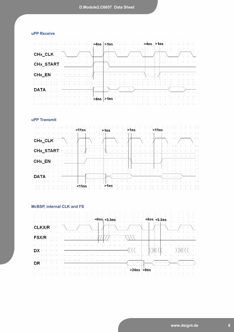
uPP Receive
uPP Transmit
McBSP, internal CLK and FS
D.Module2.C6657 Data Sheet
8www.dsignt.de

McBSP, external CLK and FS
SPI, I2C, GPIO
The level shifters used on the D.Module2.C6657 add a propagation delay of 5ns. Please add this delay to
the timings given in the TMS320C6657 data sheet SPRS814.
PCIe, SRIO
These interfaces are direct connections to the DSP. For timing information please refer to the
TMS320C6657 data sheet SPRS814.
D.Module2.C6657 Data Sheet
9www.dsignt.de

Signal Description and Connector Pinout
3.3V Supply IN, 0V Supply IN Power Supply Input
3.3V OUT, 0V OUT Power Supply to Peripheral Boards
SETUP_N, IN0_N, IN1_N Configuration Inputs: normal system startup / Setup Mode / Recovery Mode
RESIN_N System Reset Input
USB_D+, USB_D-, USB_GND, USB_VBUS USB Interface
UART_RXD/A, UART_CTS/B, UART_TXD/Y, UART_RTS/Z RS232 / RS422
ETH_TX+/TP0+,ETH_TX-/TP0- ETH_RX+/TP1+,ETH_RX-/TP1-ETH_TP2+,ETH_TP2-ETH_TP3+,ETH_TP3-
Ethernet Interface 100Base-Tx, 1000Base-T (Copper)
ETH_LED1, ETH_LED2 Ethernet external LEDs
ETH_FIN+, ETH_FIN- ETH_FOUT+, ETH_FOUTETH_FSD
Ethernet optional external Fibre-optic Transceiver (replaces Copper Interface)
SCL, SDA I²C Interface
PRGIO0..PRGIO15 bit-wise programmable GPIO
RESOUT_N External Bus Interface Reset Output
BUSCLK External Bus Interface Clock Output
INT0_N..INT2_N External Bus Interface Interrupt Inputs
BE2_N..BE3_N External Bus Interface Byte Enable Outputs (BE2_N: D{23:16] , BE3_N: D[31:24])
CS0_N, CS1_N External Bus Interface Chip Select Outputs
WR_N, RD_N External Bus Interface Read and Write Strobe Outputs
OE_N External Bus Interface Output Enable (data bus driver enable)
WAIT_N External Bus Wait Request Input (master clock input in UPP Mode)
A0..A19 External Bus Interface Address Outputs (A1..A16: port XD in UPP Mode)
D0..D7 External Bus Interface Data (Control signals in UPP Mode, not used in EMIF Mode)
D16..D31 External Bus Data (port D in UPP mode)
GPIO0..GPIO3 External Bus GPIO, routable to DSP Timer, DMA Trigger, GPIO
CLKS0, CLKR0, CLKX0, FSR0, FSX0, DATR0, DATX0 McBSP Interface Port 0
CLKS1, CLKR1, CLKX1, FSR1, FSX1, DATR1, DATX1 McBSP Interface Port 1
SPI_SIMO, SPI_SOMI, SPI_CLK, SPI_SS SPI Interface
RTC_BAT real-time clock backup battery input
FAN_PWMO, FAN_TACHIN external fan PWM output and tacho input
SYS_ALERT system alert failure output, NMI input, active low, open drain
PCIe_PETp0, PCIe_PETn0, PCIe_PERp0, PCIe_PERn0PCIe_PETp1, PCIe_PETn1, PCIe_PERp1, PCIe_PERn1
PCIe Interface
PCIe_REFCLKp, PCIe_REFCLKn PCIe Referece Clock (input or output)
PCIe_SIDE0, PCIe_SIDE1 PCIe Sideband GPIO signals
SRIO_RX0P, SRIO_RX0N, SRIO_TX0P, SRIO_TX0N, SRIO_RX1P, SRIO_RX1N, SRIO_TX1P, SRIO_TX1N
SRIO Interface
SGND Signal Return GND
D.Module2.C6657 Data Sheet
10www.dsignt.de

BUS 1 COM
Pin Signal Signal Pin Pin Signal Signal Pin
1 3.3V OUT 3.3V OUT 2 1 0V Supply IN 0V Supply IN 23 0V OUT 0V OUT 4 3 0V Supply IN 0V Supply IN 45 RESOUT_N BUSCLK 6 5 3.3V Supply IN 3.3V Supply IN 67 INT0_N SGND 8 7 3.3V Supply IN 3.3V Supply IN 89 INT1_N INT2_N 10 9 SETUP_N IN0_N 1011 SGND BE2_N 12 11 RESIN_N IN1_N 1213 OE_N BE3_N 14 13 USB_VCC USB_D+ 1415 RD_N SGND 16 15 USB_GND USB_D- 1617 WR_N WAIT_N 18 17 SGND SGND 1819 SGND CS0_N 20 19 UART_CTS / B UART_RTS / Z 2021 A0 CS1_N 22 21 UART_RXD / A UART_TXD / Y 2223 A1 SGND 24 23 SGND SGND 2425 A2 A3 26 25 ETH_TP3+ ETH_TP2+ 2627 SGND A4 28 27 ETH_TP3- ETH_TP2- 2829 A5 A16 30 29 ETH_GND ETH_GND 3031 A17 SGND 32 31 ETH_RX+/TP1+ ETH_TX+/TP0+ 3233 A18 A19 34 33 ETH_RX-/TP1- ETH_TX-/TP0- 3435 SGND D16 36 35 SGND SGND 3637 D17 D18 38 37 SCL SDA 3839 D19 SGND 40 39 SGND 4041 D20 D21 42 41 SGND 4243 SGND D22 44 43 PRGIO0 SGND 4445 D23 D24 46 45 PRGIO1 PRGIO2 4647 D25 SGND 48 47 SGND PRGIO3 4849 D26 D27 50 49 PRGIO4 PRGIO5 5051 SGND D28 52 51 PRGIO6 SGND 5253 D29 D30 54 53 PRGIO7 PRGIO8 5455 D31 SGND 56 55 SGND PRGIO9 5657 GPIO0 GPIO1 58 57 PRGIO10 PRGIO11 5859 60 59 PRGIO12 SGND 6061 62 61 PRGIO13 PRGIO!4 6263 64 63 SGND PRGIO15 64
BUS 2 EXP
Pin Signal Signal Pin Pin Signal Signal Pin
1 2 1 SGND ETH_FIN+ 23 4 3 ETH_LED1 ETH_FIN- 45 6 5 ETH_LED2 SGND 67 GPIO2 GPIO3 8 7 ETH_FSD ETH_FOUT+ 89 D0 D1 10 9 SGND ETH_FOUT_- 1011 D2 D3 12 11 1213 SGND D4 14 13 SGND 1415 D5 D6 16 15 1617 D7 SGND 18 17 SGND 1819 20 19 2021 SGND 22 21 SGND 2223 24 23 2425 SGND 26 25 SGND 2627 28 27 FAN_PWMO 2829 SGND A6 30 29 TAN_TACHIN SGND 3031 A7 A8 32 31 SYS_ALERT 3233 A9 SGND 34 33 SGND 3435 A10 A11 36 35 3637 SGND A12 38 37 SGND 3839 A13 A14 40 39 4041 A15 SGND 42 41 SGND 4243 44 43 4445 SGND DATR0 46 45 SGND 4647 CLKR0 FSR0 48 47 SPI_SIMO 4849 DATX0 SGND 50 49 SGND SPI_SOMI 5051 CLKX0 FSX0 52 51 RTC_BAT SPI_CLK 5253 SGND DATR1 54 53 SGND 5455 CLKR1 FSR1 56 55 SPI_SS 5657 DATX1 CLKX1 58 57 SGND 5859 FSX1 RESOUT_N 60 59 6061 0V OUT 0V OUT 62 61 SGND 6263 3.3V OUT 3.3V OUT 64 63 CLKS0 CLKS1 64
D.Module2.C6657 Data Sheet
11www.dsignt.de

GTP
A B C D
1 SGND SGND SGND2 PCIe_PETp0 (DSP: PCIERXP0) SGND SGND SRIO_RX1P3 PCIe_PETn0 (DSP: PCIERXN0) PCIe_PETp1 (DSP: PCIERXP1) SRIO_RX0P SRIO_RX1N4 SGND PCIe_PETn1 (DSP: PCIERXN1) SRIO_RX0N SGND5 PCIe_PERp0 (DSP: PCIETXP0) SGND SGND SRIO_TX1P6 PCIe_PERn0 (DSP: PCIETXN0) PCIe_PERp1 (DSP: PCIETXP1) SRIO_TX0P SRIO_TX1N7 SGND PCIe_PERn1 (DSP: PCIETXN1) SRIO_TX0N SGND8 PCIe_REFCLKp SGND SGND9 PCIe_REFCLKn PCIe_SIDE0 SGND10 SGND PCIe_SIDE1 SGND
Mechanical Dimensions
D.Module2.C6657 Data Sheet
12www.dsignt.de
8,4 mm Molex 71436-2164 Molex 71436-2164
4,0 mm max. component height on bottom side
COM, EXP, BUS1, BUS2, GTP connectors on bottom side, JTAG on top side
22,9
mm
1,6
mm
58,
4 m
m
86,8 mm
61,8 mm
3,5 mm
25,0 mm
83,3 mm
3,5
mm
5,1
mm
54,
9 m
m
54,
3 m
m
4,1
mm
4*d=2,8 mm
COM EXP
BUS1 BUS2
29,
2 m
m
4,9 mm
GTP
Molex 46556-114
A1
D10
1
64
1
64
6464
11
23,
0 m
m
JTAG
5,08mm
21,7
mm

Ordering Information
D.Module2.C6657 Data Sheet
13www.dsignt.de
Ordering Information
D.Module2.C6657 Dual-Core DSP module with TMS320C6657
D.Module2.C6657i Industrial grade dual-Core DSP module with TMS320C6657
DK.C6657 Complete stand-alone development kit with in-circuit emulator
DK.C6657-FMC Development package with D.Module2.C6657, D.Module2.6SLX45T FPGA
daughter card, D2.Base-FMC carrier board, and in-circuit emulator
DS.TCPIP-DM6657 Ethernet Development Support Package for D.Module2.C6657
D.SignT GmbH & Co. KG
phone: +49 (0) 2833 / 570977 • fax: +49 (0) 2833 / 3328
mail: [email protected] • web: www.dsignt.de
Marktstraße 10 • 47647 Kerken • Germany