distribution statement a approved for public … receivers, air traffic control radar, and rf test...
TRANSCRIPT
Serial No.: 09/756.239
Filing Date: 09 JANUARY 2001
Inventor: HAL L. LEVITT
NOTICE
The above identified patent application is available for licensing. Requests for information should be addressed to:
ASSOCIATE COUNSEL (PATENTS) CODE 1008.2 NAVAL RESEARCH LABORATORY WASHINGTON DC 20375
DISTRIBUTION STATEMENT A Approved for Public Release
Distribution Unlimited
PATENT APPLICATION/TECHNICAL DIGEST PUBLICATION RELEASE REQUEST
FROM: Associate Counsel (Patents) (1008.2) TO: Associate Counsel (Patents) (1008.2)
Via: (1) Hal Levitt (Code 5721) (2) Division Superintendent (Code 5700) (3) Head, Classification Management & Control (Code 1221)
SUBJ: Patent Application/Technical Digest entitled: "MULTIPLE SIMULTANEOUS OPTICAL FREQUENCY MEASUREMENT" Request for release for publication.
REF: (a) NRL Instruction 5510.40C (b) Chapter 6, ONRINST 587 0.1C
ENCL: (1) Copy of Patent Application/Technical Digest
1. In accordance with the provision of references (a) and (b), it is hereby requested that the subject Patent Application/Technical Digest be released for publication.
2. It is intended to offer this Patent Application/Technical Digest to the National Technical Information Service, for publication.
3. This request is in connection with Navy Case No. 79,276
^MRäSEK^7'
ciate Counsel (Patents]
FIRST ENDORSEMENT Date:
FROM: Hal Levittb" (Code 5721) TO: Division Superintendent (Code 5700)
1. It is the opinion of the Inventor(s) that the subject Patent Application/Technical Digest Ci^T (is not) classified and there is no objection to public release. """
j4*A ^ ks\ Jt Jem ZOoi Inventor's Signature
NDW-NRL 551/3001 (Rev. 6-89) (Page 1 of 2)

SECOND ENDORSEMENT Date:
FROM: Division Superintendent (Code 5700) TO: Classification Management & Control (Code 1221)
1. Release of Patent Application/Technical Digest (is) (is not) approved.
2. To the best knowledge of this Division, the subject matter of this Patent Application/Technical Digest (has) (has not) been classified.
3. This recommendation takes into account military security, sponsor requirements and other administration considerations and there in no objection to public release.
/$*/£ /#//??attex? Division Superintendent
THIRD ENDORSEMENT Date:
FROM: Head, Classification & Control (Code 1221) TO: Associate Counsel (Patents) (1008.2)
1. This Patent Application/Technical Digest is authorized for public release.
Head, Classification,Management & Control
NDW-NRL 5511/3001 (Rev. 6-89) (Page 2 of 2)

Applicant: Levitt PATENT APPLICATION Attorney Docket: NC 79,276
MULTIPLE SIMULTANEOUS OPTICAL
FREQUENCY MEASUREMENT
BACKGROUND OF THE INVENTION
5 Field of the Invention
The present invention is directed to electrical frequency
measurement, and particularly to a signal processing apparatus for providing
accurate temporal frequency measurement of multiple time-coincident radio
frequency ("RF") signals over a wide instantaneous bandwidth and dynamic
10 range.
Description of the Related Art
Electrical frequency measurement is a requirement for
numerous signal processing, communication, and signal measurement
systems in use today and in the foreseeable future. A wide instantaneous
15 operating bandwidth is essential in many systems. Frequency is a key
measurement parameter for the purpose of RF signal tracking,
characterization, and identification. Commercial and military applications
operating in congested RF environments must process multiple signals
simultaneously and provide measurement of selected signals while rejecting
20 other undesirable interfering signals within the operating bandwidth. Present
day applications include satellite and terrestrial communications systems,
radar receivers, air traffic control radar, and RF test equipment.
Existing equipment implement one or more frequency
measurement devices including instantaneous frequency measurement
DUG 20010215 092

Applicant: Levitt PATENT APPLICATION Attorney Docket: NC 79,276
("IFM") receivers, frequency discriminators, and channelized receivers. Each
alternative has drawbacks. For example, most frequency discriminators and
IFMs operate within a limited internal input signal dynamic range, typically
within the saturation region, and, hence, require additional circuits to
5 constrain input signals to this region. Because these devices are not
frequency channelized, they are unable to correctly resolve time-coincident
pulse-on-pulse or pulse-on-continuous wave ("CW") signals. These devices
are constrained to handle a single signal at a time. If a second signal occurs
in the same time window, an IFM cannot measure the second signal. RF
10 channelizer technology alone cannot provide sufficient frequency resolution
without incurring a high cost for the required large number of equivalent RF
filter bank elements and video circuitry, and suffer from false "rabbit ears"
triggering with such narrow filter widths. In addition, RF channelizers
provide only relatively coarse frequency measurements.
15 Furthermore, because the IFM can measure only one signal at
a time, a CW wave (i.e., a signal that is very long in pulse width) can hinder
the ability of an IFM to measure the remaining environment. Thus, by
driving an IFM with a strong signal that is turned on continuously, the IFM
becomes unable to operate and collect other threats in the environment.
20 A U.S. patent of interest includes U.S. Pat. No. 5,682,238 to
Levitt et al. (the subject matter of which is incorporated herein by reference),
which discloses a signal processing apparatus with an optical phase
measurement processor that provides phase difference measurements of
multiple signal inputs.
Applicant: Levitt PATENT APPLICATION Attorney Docket: NC 79,276
SUMMARY OF THE INVENTION
The present invention measures frequency of multiple, time-
coincident (i.e., two or more signals in which a portion of one signal duration
coincides in time with a portion of one or more other signal durations) RF
5 signals within a wide instantaneous input bandwidth and dynamic range. In
one embodiment of the present invention, RF delay line 104 circuits are
combined with a single optical processor 200, a spatial-domain phase
measurement technique, and associated algorithms to provide simultaneous
fine frequency measurement resolution that is maintained over the entire
10 dynamic range. RF delay line 104 and power splitter 102 components
provide two wideband RF inputs for the optical processor 200, one time-
delayed relative to the other. Channelizer processing circuitry utilizes optical
processor photodetector outputs to perform signal detection, coarse frequency
estimation, fine frequency estimation, frequency and phase calibration, and
15 combination of coarse and fine frequency for final output.
Multiple signal inputs of interest are simultaneously detected
and measured in frequency, and optionally, other time-domain parameters.
Basic frequency measurement occurs through two concurrent processes -
detection of signal presence with (1) coarse frequency measurement, and (2)
20 fine frequency measurement. Both functions are performed in a single
measurement cycle.
Detection and coarse frequency measurement are achieved
through modulator induced optical beam deflection onto a photodetector
array 212, wherein active detector positions directly correspond to incident
25 RF signal spectral components. Within a corresponding photodetector
element bandwidth, fine frequency is obtained by measurement of relative
phase difference between the original RF0 and a delayed version RF1 of the
Applicant: Levitt PATENT APPLICATION Attorney Docket: NC 79,276
incident RF signal, effectively through frequency to phase translation. This is
accomplished by RF modulation of two optical input beams 205 followed by
projection of the modulated beams to produce an optical interference pattern
upon the photodetector elements. The resulting spatial intensity pattern phase
5 variation is decoded by an efficient spatial sampling technique and associated
algorithms, such as those employed in the '238 patent.
The delay time is selected to achieve a specified fine
frequency resolution and provide unambiguous phase measurement within
one coarse frequency resolution width. The number of photodetector
10 elements along the frequency deflection axis of the photodetector array 212,
instantaneous operating bandwidth, in conjunction with other opto-electronic
design parameters determine the effective coarse frequency resolution.
The photodetector outputs are applied to a frequency encoder
400 circuit to correct the raw phase and amplitude (or magnitude) data
15 offsets, detect and locate active signals within the array 212, convert phase to
fine frequency, and finally, concatenate coarse to fine frequency for readout.
The encoded combination of coarse frequency with fine frequency
discriminator output permits precision frequency measurement over the entire
system bandwidth. Additionally, multiple time-coincident RF input sources,
20 which are resolvable in frequency, can be processed in parallel using the
present invention.
Unlike commercial electronic frequency discriminator and
IFM devices, the present invention permits frequency measurement of
multiple, time-coincident, and continuous wave signals, which is a shortfall
25 of these single channel devices. The present invention has a separation at the
frequency subchannels, and each subchannel performs the frequency
discriminator type operation simultaneously. Most frequency discriminators
and IFMs function similar to only one subchannel of the present invention,

Applicant: Levitt PATENT APPLICATION Attorney Docket: NC 79,276
thereby processing the composite input bandwidth without first separating
individual RF signals. This often leads to gross frequency measurement
errors under time-coincident signal conditions.
Compared to other multi-channel techniques, such as RF filter
5 banks and channelized receivers, the present invention provides increased
frequency measurement resolution using intrachannel phase-based
techniques, with sustainable accuracy across the entire operating bandwidth
and temperature range through continuous phase offset correction. Current
frequency discriminator and EFM devices must operate with a saturated input
10 and therefore function (internally) over a limited amplitude dynamic range to
attain accurate measurements. In contrast, the present invention functions
correctly over a much wider dynamic range, limited principally by noise and
photodetector saturation. This extends the achievable system dynamic range
and eliminates RF limiting circuitry, resulting in reduced system cost and
15 improved performance.
Additionally, coherent (IF output) or incoherent (video output)
signal detection can be utilized in the present invention. Incoherent or power
detection simplifies subsequent signal processing hardware requirements,
operating at relatively narrow video bandwidth. In contrast, coherent or
20 heterodyne detection requires more complex processing hardware operating
at intermediate frequencies ("IF"), but, in principle, can achieve a larger
dynamic range. A typical coherent approach requires optical carrier mixing
and filtering operations to convert the RF modulated optical photodetector
output to a corresponding electrical IF signal, which must then be time-
25 domain processed to measure frequency. The preferred embodiment
discussed herein utilizes incoherent signal detection methods to illustrate a
relatively simple and low cost approach to frequency measurement.
Applicant: Levitt PATENT APPLICATION Attorney Docket: NC 79,276
These, together with other advantages that will be
subsequently apparent, reside in the details of construction and operation as
more fully hereinafter described and claimed, reference being had to the
accompanying drawings forming a part hereof, wherein like numerals refer to
5 like parts throughout.
BRIEF DESCRIPTION OF THE DRAWINGS
FIG. 1 is a schematic block diagram of a preferred
embodiment of the multiple simultaneous optical frequency measurement
apparatus of the present invention;
10 FIG. 2 is a schematic block diagram of the channelized optical
phase measurement (COPM) module of FIG. 1 of the present invention;
FIG. 3 is a flow diagram of photodetector video processing
within the COPM of FIG. 2;
FIG. 4 is a flow diagram of processing within the frequency
15 encoder module of FIG. 1 of the present invention;
FIG. 5 is a schematic block diagram of the multiple
simultaneous optical frequency measurement apparatus of the present
invention in an exemplary radio frequency measurement application; and
FIG. 6 is a graph of frequency measurement performance of
20 the apparatus of FIG. 1.
DESCRIPTION OF THE PREFERRED EMBODIMENTS
FIG. 1 illustrates a schematic block diagram of a preferred
embodiment of the present invention, which is a multiple simultaneous
optical frequency measurement ("MSOFM") apparatus 100. In FIG. 1, an RF

Applicant: Levitt PATENT APPLICATION Attorney Docket: NC 79,276
input signal is split into two separate paths by an RF power splitter 102. One
path incurs an additional fixed time delay relative to the other as a
consequence of a delay line 104. The delayed RF1 and direct RFO (non-
delayed) signals then serve as inputs to a module providing multiple
5 concurrent measurement and readout of coarse frequency, phase, and
optionally magnitude, on a (coarse) frequency channelized basis. Preferably,
the channelized optical phase measurement ("COPM") module 200 of the
'238 patent is used, which extracts phase and amplitude of N parallel
frequency channels simultaneously.
10 A frequency encoder 400 corrects phase and amplitude (or
magnitude) data offsets, detects and locates active signals within a
photodetector array 212 of the COPM 200 (described below), converts phase
to fine frequency, and, finally, concatenates or otherwise combines coarse to
fine frequency for readout, along with a signal indicating the data is valid and
15 ready to be output. Periodic calibration interlaced or overlaid with normal
operation (by employing an internal signal source) sustains system accuracy
over time and temperature, and significantly reduces RF and optical
component phase match requirements.
Other types of input signals may alternatively be used, such as
20 sound, heat, light, electrical voltage, or any other measurable quantity capable
of modulating or otherwise altering a carrier signal to impose frequency,
phase, and optionally amplitude information.
Also, the delay line 104 lengths may vary, such that for the
single MSOFM 100 system implementation, phase ambiguities can be
25 avoided within a single coarse channel bandwidth. In addition, other
technologies for the delay line 104 (e.g., a bulk acoustic wave delay line) and
the power splitter 102 may be used. Although these components are depicted
Applicant: Levitt PATENT APPLICATION Attorney Docket: NC 79,276
within the RF signal input path of the preferred embodiment, they may
alternatively be implemented in the optical path.
FIG. 2 illustrates a schematic block diagram of the COPM
module 200 of the present invention. The COPM module 200 provides phase
5 and frequency measurements for each frequency bin or channel,
corresponding to a sub-band of the composite RF operating bandwidth. A
beam splitter 204 divides an optical beam from a laser 202 into two mutually
coherent optical beams 205. The two optical beams 205 propagate through
two separate channelizer circuits, preferably two acousto-optic Bragg cell
10 modulators 206, that separate the input RF bandwidth into separate coarse
frequency channels. Alternatively, a single Bragg cell 206 fabricated with
dual RF transducers may be used. The Bragg cell 206 optical aperture
spacing is independent of RF frequency or delay line 104 time.
Input signals RF0 and RF1, corresponding to direct and
15 delayed RF environment, respectively, are injected into the Bragg cells 206.
Within the Bragg cells 206, each light beam 205 is modulated by the
frequency and phase of its associated RF input, imposing incident RF signal
amplitude and frequency (and inherently phase) onto each optical carrier.
Thus, a relative phase difference at the IF input is replicated in the Bragg cell
20 206 optical outputs 207.
In addition to optical carriers, the carrier may also be
represented in other forms (e.g., radio waves) or other frequency spectral
ranges as well. Thus, for example, RF applications may use microwave,
millimeter-wave bands, or optical carriers at infrared or ultraviolet
25 wavelengths.
Upon exiting the Bragg cells 206, the two optical beams 207
interfere spatially to develop an interference pattern. This optical interference
pattern is Fourier-transformed by a Fourier Transform lens 210 and imaged
8
Applicant: Levitt PATENT APPLICATION Attorney Docket: NC 79,276
onto an area detector or photodetector array 212, providing a spectral
decomposition of the incident RF spectrum.
One axis (Y-axis) of the photodetector array 212 corresponds
to frequency channel number ("Frequency Chan#"), while the orthogonal axis
5 (X-axis) corresponds to relative signal phase (and amplitude) information in
spatial form as a sinusoidal intensity pattern. The two optical beams are
deflected along the Frequency Chan# axis at an angle approximately
proportional to the incident RF signal frequency. Because both RF inputs,
RFO and RF1, are identical with the exception of a time delay, their spectral
10 intensity decomposition patterns are also identical along the Frequency
Chan# axis. Thus, the resulting photodetector image intensity modulation
pattern is two-dimensional, with phase interference occurring along the phase
or X-axis and the RF signal Fourier transform occurring along the Frequency
Chan# axis.
15 At a Frequency Chan# axis position associated with the RF
frequency of the signal to be measured, a differential phase corresponding to
the time delay between RF inputs, and thereby proportional to frequency, is
imposed onto the optical beams 205. This results in an interference pattern
spatial phase proportional to input RF frequency, which is subsequently
20 converted to a fine frequency estimate by algorithms implemented within the
frequency encoder 400.
Each coarse channel bin unambiguously resolves frequency to
within one phase rotation. This is accomplished by using either or both of the
following exemplary techniques: (1) reducing coarse channel width to less
25 than one equivalent fine frequency phase rotation, and (2) utilizing adjacent
coarse channel response magnitudes to interpolate within one channel. Other
alternative methods may be employed to satisfy this objective.

Applicant: Levitt PATENT APPLICATION Attorney Docket: NC 79,276
In a preferred implementation, the COPM 200 uses an
efficient three-point spatial sampling scheme. The photodetector array 212
phase axis contains three detector elements that sample the interference
pattern at fixed spatial locations chosen to most efficiently transform the three
5 photodetector voltage outputs representing optical intensities to RF phase
difference using a simple phase extraction algorithm 306 (FIG. 3).
The embodiment shown in FIG. 2 depicts three outputs from
each photodetector array 212 row (corresponding to Frequency Chan# i, for i
from 1 to N) being applied to one of a multitude of phase extraction
10 processors 300, each applying the aforementioned algorithm 306 to calculate
a phase difference between the two RF inputs. An advantage of using three
(or more) detector outputs for phase measurement is the added capability of
measuring RF signal magnitude (or absolute amplitude), which is necessary
for subsequent threshold detection and centroid operations performed within
15 the frequency encoder 400 (described below).
Use of the three-detection element spatial sampling format and
algorithm provides high measurement accuracy and built-in correction for
detector amplitude offsets, which vary as a function of input and reference
carrier signal strength. User of fewer (e.g., three) spatial sampling-detection
20 elements also results in higher speed and less complex implementation of the
apparatus.
The detectors of the photodetector array 212 may be a single
integrated device, or the detectors may be multiple separate detectors
adjacently positioned at the Fourier transform plane or remotely located, such
25 that Fourier transform plane information is transferred to appropriate detector
elements. One example is to position an array of optical fibers at the Fourier
plane, the fibers effectively transporting the light intensity pattern to a
remotely located array of individual photodetectors.
10

Applicant: Levitt PATENT APPLICATION Attorney Docket: NC 79,276
The spatial intensity pattern phase variation is preferably
decoded by the COPM 200 optical processor of the '238 patent to provide
coarse frequency, phase, and amplitude measurement functionality. The
COPM 200 performs coarse RF channelization by, for example, a dual
5 transducer acousto-optic Bragg cell modulator within the optical processor,
which is an operation analogous to an RF filter bank, with filter output
detection accomplished by the array 212 of photodetector elements.
Video and A/D conversion circuits (not shown) then encode
individual photodetector element outputs into a binary-encoded digital format
10 for subsequent digital processing. After digitization of photodetector video
output, detection circuitry recognizes signal presence based on photodetector
output level, or signal magnitude computation, and provides a coarse
frequency estimate. Electrical phase measurements are then performed on the
photodetected two-beam optical interference pattern using an optical spatial
15 sampling technique.
FIG. 3 is a flow diagram of photodetector video processing
within the phase extraction processors 300 of the COPM 200. In FIG. 3, "N"
denotes the number of photodector elements along the Frequency Chan# axis.
In this embodiment, three photodetector elements are used for phase
20 measurement along the phase axis. A gain correction module 302 and an
offset correction module 304 perform gain correction and offset correction,
respectively, on the photodetector outputs (video) before processing by the
extraction algorithm 306 for phase and amplitude. Not shown, but implicit, is
A/D conversion of the video prior to processing for phase and amplitude.
25 The operations of the phase extraction processors 300 may be implemented in
either software, hardware, or a hybrid of both.
The configuration of RF delay line 104 and power splitter 102
circuits driving COPM 200 inputs corresponds to a classical delay-line
11

Applicant: Levitt PATENT APPLICATION Attorney Docket: NC 79,276
frequency discriminator at each photodetector (coarse) frequency channel
output. Discriminator operation is characterized by production of a variable
relative phase difference between delayed and non-delayed signal paths
linearly proportional to input frequency. COPM 200 optical processing
5 translates incident electrical (time-domain) phase difference to a spatial
image pattern retaining phase information sampling by three or more
photodetectors at each frequency channel position.
FIG. 4 is a flow diagram of processing within the frequency
encoder 400 of FIG. 1. A phase offset correction module 402 receives phase
10 outputs from the COPM 200 and performs phase offset correction and coarse
frequency offset corrections on a bin-to-bin basis. The corrected phase values
are converted to fine frequency by a phase to fine frequency module 410.
The phase to fine frequency module 410 provides high
resolution interpolation within a coarse channel bandwidth, representing the
15 primary contributor to overall system frequency measurement performance.
Within the phase to fine frequency module 410, measured phase difference is
transformed to fine frequency shift (in Hertz) from an arbitrary reference, as
given by the following equation:
AF- A0
20 T-360 (1)
where,
LQ=measured phase difference (degrees), T=time delay (sees),
360=conversion constant (degrees/Hertz).
To avoid fine frequency measurement ambiguity, the delay
line 104 (FIG. 1) time is chosen to constrain phase shift to within +/- 180
12

Applicant: Levitt PATENT APPLICATION Attorney Docket: NC 79,276
degrees corresponding to +/- 0.5 coarse bin frequency width about the bin
center frequency.
An amplitude offset correction module 404 receives amplitude
outputs from the COPM 200 and performs amplitude offset correction. Phase
5 offset correction and amplitude offset correction are achieved as necessary by
subtraction of calibration offsets stored in memory associated with a
particular coarse frequency channel.
A detection logic module 406 receives the corrected amplitude
values and compares coarse channel amplitude to a predetermined threshold
10 for detection of signal presence. After detection of signal presence, centroid
logic operations within a frequency channel centroid logic module 408
determine the coarse frequency as the primary active channel within
consecutive active channels.
A frequency formatter module 412 receives the fine frequency
15 measurement from the phase to fine frequency module 410 and the coarse
frequency measurement channel number (or index) from the frequency
channel centroid logic module 408. The coarse frequency channel index is
converted to a coarse frequency value (e.g., in MHz) within the frequency
formatter 412. Alternatively, the coarse frequency channel index may be
20 converted within the frequency channel centroid logic module 408. The
calculated fine frequency is summed within the frequency formatter 412 to
the coarse initial frequency associated with the active centroided coarse
frequency channel number. The delay line 104 time is chosen to limit phase
excursions to less than 360 degrees within a coarse channel bandwidth,
25 removing the requirement for phase ambiguity resolution circuitry.
Finally, the frequency formatter 412 optionally uses the RF
band number obtained from an RF downconverter 504 (FIG. 5) to correct
coarse frequency offset, thereby selecting a starting frequency offset from, for
13

Applicant: Levitt PATENT APPLICATION Attorney Docket: NC 79,276
example, circuits (such as calibration tables) embedded within the frequency
formatter 412. The RF band number is used to sum a fixed global RF
frequency offset to the current IF frequency estimate, thereby extending
operational receiver measurement range to the entire input RF bandwidth.
5 The frequency formatter module 412 outputs a "valid" signal indicating the
data is valid and ready to be output, along with the summed frequency.
The frequency encoder 400 may be implemented in either
software, hardware, or a hybrid of both. For example, look-up tables and
sums may be used, such as a look-up table for phase to fine frequency
10 determination. Also, phase offset correction and amplitude offset correction
(i.e., calibration values) may be implemented as tables in memory to convert
from relative numbers to actual values. For example, for amplitude, the
correction is for flatness. The amplitude measured is a relative number, and
the actual amplitude is the measured amplitude plus an offset.
15 The frequency formatter module 412 generates the final
frequency for readout by, for example, concatenation of coarse and fine
frequency, or summation of absolute starting frequency band number, coarse
frequency offset to the band starting frequency, and fine frequency offset
relative to coarse frequency. The band number may be determined from a
20 look-up table (e.g., band #1 may correspond to 2,000 MHz). For speed, the
frequency formatter module 412 is preferably implemented in hardware
using, for example, a digital adder or digital tables.
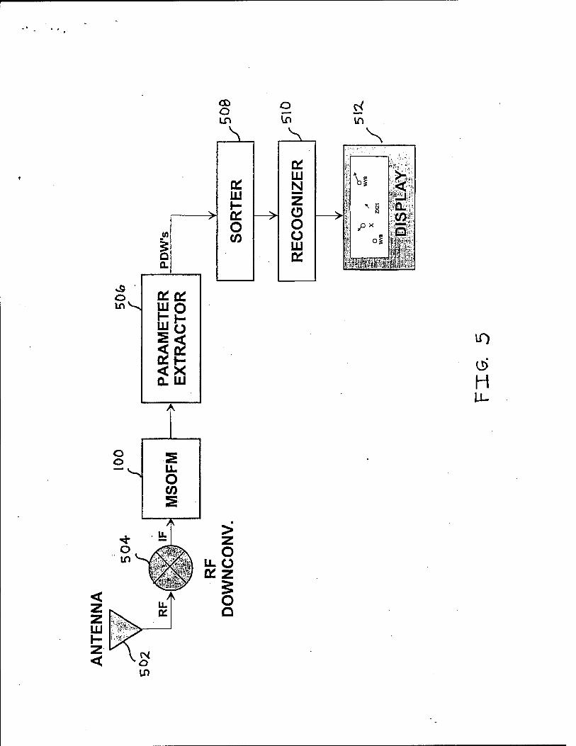
FIG. 5 is a schematic block diagram of the multiple
simultaneous optical frequency measurement apparatus 100 of the present
25 invention in an exemplary RF receiver application. An RF bandwidth
containing multiple input signals of interest propagating in free-space is
acquired by a reception antenna 502. An RF downconverter 504 then
frequency translates the RF bandwidth to an appropriate IF band for injection
14

Applicant: Levitt PATENT APPLICATION Attorney Docket: NC 79,276
into the present invention (i.e., the MSOFM) 100. The MSOFM 100 detects
signal presence and measures signal parameters, primarily that of electrical
frequency, for each signal in the active instantaneous IF bandwidth.
The MSOFM 100 outputs the measured signal parameters to a
5 conventional parameter extractor 506. The parameter extractor 506 formats
these (conceptually) parallel data patterns of signal parameters into pulse
descriptor words (PDWs). Each PDW corresponds to a single measurement
event. For each detected incident signal (e.g., radar) pulse, parameters for
passive radar signal detection (e.g., coarse frequency, fine frequency, time of
10 arrival (TOA), amplitude, and pulse repetition interval (PRI)) are measured,
then formatted into a digital description of the single RF pulse event as a
PDW, emphasizing composite fine frequency. The PDWs are processed by
algorithms within a conventional signal sorter 508 to coalesce multiple
isolated PDWs into a consolidated parametric description of the signal system
15 type. A conventional recognizer 510 then database-associates the
consolidated parametric description to a specific signal identification (ID)
code for readout on a display 512. Parameter extractors, sorters, and
recognizers are typical subsystem components of electronic support systems
receivers and radar warning receivers (RWR), such as the AN/ALR-67 RWR.
20 The present invention has been experimentally demonstrated
for the preferred embodiment. FIG. 6 is a graph of cumulative phase and
frequency accuracy measurements. Deviation from a linear fit is
representative of calibrated frequency error. Using a 29.04 nanosecond delay
line, measured frequency error was less than 0.25 MHz over a 34 MHz
25 unambiguous range. Frequency measurement linearity with input frequency
was verified over a 50 MHz range (one coarse channel) in 1 MHz steps.
These results indicate the present invention is useful in numerous practical
applications.
15

Applicant: Levitt PATENT APPLICATION Attorney Docket: NC 79,276
The present invention provides many advantages over the
prior art. EFM technology lacks multiple signal handling capabilities, while
RF channelizers provide relatively coarse frequency measurements. Unlike
commercial electronic frequency discriminator and IFM devices, the present
5 invention permits frequency measurement of multiple, time-coincident, and
CW signals. Compared to multi-channel techniques such as RF filter banks
and channelized receivers, the present invention provides increased frequency
measurement resolution using intrachannel phase-based techniques, and
sustainable accuracy across the entire operating bandwidth and temperature
10 range through continuous phase offset correction.
Additionally, current frequency discriminator and IFM devices
must function (internally) over a limited amplitude dynamic range to achieve
acceptable measurement accuracy. In contrast, the present invention
functions correctly over a much wider dynamic range, limited primarily by
15 noise and photodetector saturation. This extends the achievable system-level
dynamic range and simplifies the system design by eliminating RF limiting
circuitry requirements. The resulting compact size, low power consumption,
and reduced complexity increases system mean time before failure (MTBF)
to reduce operational cost.
20 In the preferred embodiment, several optimizations may be
identified as characteristic of the present invention in general. First, a single
apparatus performs signal detection and coarse/fine frequency measurement,
avoiding additional delay lines and associated cueing circuitry typically
required to coordinate separate coarse and fine frequency measurement
25 assets. Also, a preferred delay time value may be chosen to provide enhanced
frequency accuracy, yet avoid phase ambiguities throughout a wide
instantaneous bandwidth, which is a feature exploited from channelized
16

Applicant: Levitt PATENT APPLICATION Attorney Docket: NC 79,276
optical phase measurement. In addition, a continuous calibration scheme
provides phase offset correction over bandwidth and temperature to
significantly reduce component phase matching requirements of the RF and
optical system elements. Further, low system complexity, as previously
5 described, is expected to result in reduced size, weight, power consumption,
and cost over alternative approaches.
Incoherent or coherent detection is possible using the present
invention. Incoherent (power) detection, depicted in the preferred
embodiment, simplifies subsequent signal processing hardware requirements
10 by performing parameter measurements at a relatively narrow video
bandwidth. In contrast, typical coherent signal detection requires more
complex processing hardware for operation at intermediate frequencies, but
potentially has a larger dynamic range.
Alternative embodiments of the present invention address
15 varying application requirements, such as increased fine frequency resolution,
increased bandwidth, or alternate photodetector array 212 readout/frequency
encoder 400 configurations, among others.
To achieve increased system bandwidth, multiple instances of
the present invention may be configured in end-to-end fashion, each
20 frequency offset from its neighbor to obtain a composite bandwidth
equivalent to the sum of individual bandwidths of the present invention.
Improved fine frequency resolution can be achieved using
multiple parallel-configured instances of the present invention, each operating
over an identical instantaneous bandwidth, but differing in delay line 104
25 time. In this configuration, individual MSOFM 100 units have carefully
chosen delay times that may independently provide ambiguous frequency
measurements. Subsequent composite processing of the multiple independent
17
Applicant: Levitt PATENT APPLICATION Attorney Docket: NC 79,276
frequency measurements then resolves the ambiguities, using techniques
borrowed from the field of RF interferometry. Maximum achievable
frequency measurement resolution using this technique typically corresponds
to an (ambiguous) frequency measurement resolution of the MSOFM 100
5 instance having the longest time delay.
Also, the number of coarse frequency channels and overall
instantaneous bandwidth is arbitrary. In the preferred embodiment, coarse
frequency channels are assumed to be equally spaced and sequentially
ordered, but this is not a requirement.
10 The many features and advantages of the invention are
apparent from the detailed specification and, thus, it is intended by the
appended claims to cover all such features and advantages of the invention
which fall within the true spirit and scope of the invention. Further, since
numerous modifications and changes will readily occur to those skilled in the
15 art, it is not desired to limit the invention to the exact construction and
operation illustrated and described, and accordingly all suitable modifications
and equivalents may be resorted to, falling within the scope of the invention.
18
MULTIPLE SIMULTANEOUS OPTICAL
FREQUENCY MEASUREMENT
ABSTRACT OF THE DISCLOSURE
A signal processing apparatus for providing concurrent electrical
frequency measurements of multiple, time-coincident signal inputs. In one
embodiment of the present invention, an input signal is received that contains
a plurality of individual signals independent of each other in frequency,
phase, and electrical amplitude. A power splitter splits the input signal into
two separate input signals. A delay line introduces a time delay to one of the
two separate input signals. Two Bragg cells within a channelized optical
phase measurement (COPM) device modulates two optical carrier signals
with the delayed and non-delayed input signals, respectively, separating the
modulated delayed and non-delayed input signals into multiple time-
concurrent frequency channel signals. Upon exiting the Bragg cells, the two
optical beams interfere spatially to develop an interference pattern along the
phase and frequency channel number axes of a photodetector array. The
resulting spatial intensity pattern phase variation is decoded to provide coarse
frequency, phase, and amplitude measurements. A frequency encoder
receives the photodetector outputs, corrects phase and amplitude data offsets,
and converts phase to fine frequency. Finally, the frequency formatter
concatenates coarse to fine frequency for readout.

A A tf)
«*■*
/ '5 G a £
O 3 HI O < a:
t
1 > LL
FR
EQ
E
NC
OD
ER
s ^ V CD
/ ̂ ^ k >
> ™
d)= ü O
4fc o
M -9 ^ c ci.
2o s HI
/Z LL. LL < a.
E *-- o
o 2 O
»4— c£
ti
ü
IL A > < QC ^-^
** o >-
•
^ü oc
UjZ QJ
>s
~£ Q^UJ Mir
IE 2^
•"'»"•f:?i.^-':' . •■:'; 5.äE*rtg
>* \
CO
a c LL — li-
tt

* 5 i» s
o o
\
H U-

rn
CO
H
£ ■o o ° o ®
a. >

H U-
LU
10
H

(sBap) aseqd eAjjeiniJuno
V6Z .c
W7. ? in
SZ3 XJ
ttZ
nz o 11
XrZZ n. o nz Cfl <D
\rZZ (0
-C ?.Z7, Q.
(ZHW) J0Ji3
H