distribution category uc-63 no. 6329-27 … · due to an opaquing layer forming on the cell...
TRANSCRIPT
DRL 175 DOE/JPL-956205-84/8Distribution Category UC-63
Quarterly Technical Progress Report
No. 6329-27
on the
DEVELOPMENT OF METALLIZATION PROCESS
FSA Project, Cell and Module Formation Research Area
For the Period Ending
June 30, 1984
Contract 956205
Prepared by:
Alexander Garcia III
Approved by :
Nick MardesichManager , Advanced Programs
SPECTROLAB, INC.12500 Gladstone Avenue
Sylmar, California 91342
July 1984
The JPL Flat Plate Solar Array Project is sponsored by theU.S. Department of Energy and forms part of the Solar Photo-voltaic Conversion Program to initiate a major effort towardthe development of low-cost solar arrays. This work was per-formed for the Jet Propulsion Laboratory, California Instituteof Technology by agreement between NASA and DOE.
https://ntrs.nasa.gov/search.jsp?R=19840025959 2018-08-09T09:28:56+00:00Z

This report was prepared as an account of work sponsoredby the United States Government. Neither the UnitedStates nor the United States Department of Energy, norany of their employees, nor any of their contractors,subcontractors, or their employees., makes any warranty,express or implied, or assumes any legal usefulnessof any information, apparatus, product or process dis-closed, or represents that its use would not infringeprivately-owned rights.

ABSTRACT/SUMMARY
New pastes were evaluated that contained additives to aid in the
silicon-to-metallization contact. None were completely success-
ful. A reevaluation of the molybdenum oxide paste and the two-
step screen printing process was done. The oxide paste did not
show promise. The two-step process enabled soldering of the
cells but the cells still had a high series resistance. Pastes
are on order from a different manufacturer.

TABLE OF CONTENTS
Section Title Paqe
ABSTRACT/SUMMARY i
1.0 INTRODUCTION 1
2.0 TECHNICAL DISCUSSION 2
3.0. CONCLUSION AND RECOMMENDATIONS 12
4.0 ACTIVITIES PROJECTION 12
-11-
Section 1.0
INTRODUCTION
The objective of this contract is the optimization, evaluation,
and demonstration of a novel metallization applied by a screen
printing process. The process will be evaluated on both CZ
and non-CZ silicon wafers.
-1-

Section 2.0
TECHNICAL DISCUSSION
Based upon the SEM work done on the heated stage at Mircoscopy
Research Laboratories, Inc. a set of experiments was done using
the L paste and sintering for long periods of time at lower
temperatures without drying. It was hoped that the nonwetting
of the molten tin particles was caused by an oxide which would
be broken down in time by reaction with hydrogen. Cells were
printed, dryed and placed in the sintering furnace under H- at
400°C. After 4 hours in the furnace cells did not show signs
of sintering. Two new pastes were procured from Electrink.
Table 1 shows the formulations. These formulations were based
on experience at Electrink on silver inks. Paste S is similar
to Paste J with silver flake added and Paste T has bismith
added. The printed cells were sintered at temperatures of up
to 650°C but did not show good curve shape. Typical light and
dark curves are shown in Figures 1 and 2. Higher temperatures
and longer times produced low shunt resistances. Both S and T
behaved in a similar fashion.
More experimentation was done on the molybdenum oxide paste
(Paste M). Sintering temperatures up to 825°C under H2 were
used. The best cell IV curves are shown in Figures 3 and 4.
Cells fired at higher temperatures showed severe shunts. The
low short circuit current is difficult to explain and may be
due to an opaquing layer forming on the cell surface. Cells
fired at temperatures of 825 and 850°C showed metallic-like
-2-

Table 1
PRODUCT INFORMATION
Formulation % by Weight
Item F-86 . F-87
Vehicle Formulation
Item • V-38
a-terpineol . 43.62
Butyl Carbitol Acetate 43.62
Ethyl Cellulose N-14 . 9.76
Thixatrol ST 3.00
Titanium Hydride (TiH2) .55 .55
Molybdenum Powder 14.40 14.40
Tin Powder 57.60 57.60
Frit L1571A 4.45 4.45
Silver Flake Type C ' 8.00
Bismuth Powder - 8.00
Vehicle V-38 15.00 15.00
Identification S • T
-3-

Table 1 (continued)
Frit Composition - % by Weight
Item Frit L1571A
PbO
B2°3
sio2
60
30
10
Material
Titanium Hydride (TiH2)
Silver Flake
Molybenum Powder
Tin Power 325 Mesh
Frit No. L1571A
a-terpineol
Butyl Carbitol Acetate
Ethyl Cellulose
Thixatrol (thickner)
Elvacite (acrylic resin)
Bismuth Powder
Materials Sources
Designation
77113
C
Source
Alfa-Ventron, Danvers, MA
Metz Meta-lurgical, Plainfield,Nj
280/325 GTE Sylvania, Towanda, PA
00352 Alfa-Ventron, Danvers, MA
L1571A . Americal Porcelain Enamel Co.Muskegan, Mich.
TX 75 MCB Chem. Cincinnati, OH
BX 1722 MCB Chem. Cincinnati, OH
N-14 Hercules, Wilmington, DE
ST NL Industries, Hightstown, NJ
2042 Dupont, Wilmington, DE
00046 Alfa-Ventron, Danvers, MA
-4-

v .+
o
X
+ <H
U
ac
Hrr*
100
90
80
70
60
50
40
30•
20
10
Fiq
••
-
—
:
-
li
X
i
1
1
«>/
11
4.AR C
*ECTI
\
\
IONVERTER E I^^^
1
i
\
CURVE
7O&4S Q C FORM 3001
9VLMA ». CA L/FORNM^^ATE: . . . w1 - 7~J? y
PROJECT:
sC
E
D
RIAL N
CELLC5V
SOURCE:
DCC
TEST
TES7
lsc=
PMp
)LLIM
'TEM
'NO.
^>.
0
lr3
\..f .. _ ̂ ^**^^
^ L 2_C ,^s
/IODULE D PANEL DESIGNATION:
•5'. 3 -5
DSUN D TUNGSTEN D XENON
A
P
TED D UNCOLLIMATED
°r °
Pt
V
= 1
?octoc--
K
. NO.=
F
1 1 II 1 ~Tl 1 1 ! 1
1
fc
^^
|-
1
ure 1
*lv>^ i
j1
>
\
I1
i
*N
1
1
^̂
i
1
i
^
j
I
11
t
i
S^
tz '
1 1
^1
j
l
^
i
1
1
1
I
| ! ,
t j
! I 1
S —1
n 1 t ^
+_J —
i
— r
ii
i
'
1
I
j
i
1i ;
i
j1
i
i! i
1
! 1
Li
^s^ i
i
\-*~
1
1
i
t
1
!
i
!
1
1 !i
1
j
1 1
1 I !1 j
i
i
1
1
j
i
11
ii :
1
1{
! ~~ '
11
1!
.'
1
1
1 i
11
t
i
1 i
1 ji
i
j
j
t1
1
!
1
i
!ji
1
~J-'-
1:li
1 ...
;w'0 0.1 0.2 0.3 -5- 0.4 0.5 0.6 0.7
VOITAGF (VOLTS Y 1 . )
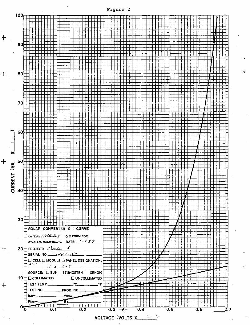
Figure 2100
+
+s
111ceOS=3U
SOLAR CONVERTER E I CURVE
SPECTROLA3 Q c FORM 3001
SYLMAR. CALIFORNIA DATE: 3-7-$
U CELL U MODULE D PANEL DESIGNATION:<f£f"
SOURCE: DSUN D TUNGSTEN D XENON
D COLLIMATED D UNCOLLIMATED
TEST TEMP.:
TEST NO.
lsc=
PMp
PROC. NO.
Voc
0.3 -6-
VOLTAGE (VOLTS
0.7

S~~*
oi-H
X
N̂ *-
H
Uatac
100
90
80
70
60
50
40
30
20
10
0
Figure 3
•
-
-
i i
i L
.I i
ll i
i i
i i
n i
i i
i
••
—••
i
i
•M M
•m m =•• =s
SOLAR CONVERTER E 1
SPECTROLAB Q c F
SYLMAR. CALIFORNIA DATE
PROJ ECT: 7>? &*^2
SERIAL NO.
M
1
^•i•K
^ iV M mM ta
1
CURVE
ORM 3001
- *,w.y7aa'
r' 3-f J-<?
D CELL O MODULE O PANEL DESIGNATION:
SO
D(
TE!
TE:IscPM
URCE
:OLLI3TTE
3TNC
: C
MA
MP
DSUN D TUNGSTEN D XENON
fED D.
PF
\
E
IOC
'oc=
W
UNCOLLIMATED
'C
VI
"I
~1 ! i i i i i
~i
m
1 1
C
i! 11 1
i !
!
j
«
i
^ •*
i
11
1
i:1
•m «
iI
1 !1
1
* 5
t
»*L,
1
i1
i
j
^ «^J
X
I ii
1
1
!
!
i
Ii t
—
' L
^SL
_|
1
k\I
\̂f ii
i
I• 1
1 !
I
! t j! : '
i
!|
i
i
1
i
\Jv
-4—— v —i V i
1VV\l•t
:\
i
1
1
1
'< '
i1
{
1
' 'I 1
! ! V ;-M 1-
1 i j\ii
1 \| i 1
~ Tv
1
I
Iii
1
1
1 !
1
t
1
!
1
1 1' I 1
ii
1
.— r-
0 0.1 0.2 0.3 -7- 0.4 0.5 0.6 0.
VOLTAGE (VOLTS y l . )7

100Figure 4
= SOLAR CONVERTER E I CURVE
J SPECTROLAB Q c FORM 3001
D CELL D MODULE D PANEL DESIGN
-j SOURCE: DSUN DTUNGST
H D COLLIMATED
-| TEST TEMP.:
j TEST NO
Isc
-8-
VOLTAGE (YOLTS x.0.5 0.6 0.7
grid patterns which were solderable. However, none of the
solderable cells had measurable IV curves. Spectrolab has
been unable to reproduce earlier research done on this paste
system.
The use of a two-step screen printing sequence was reexamined.
Cells were first printed with J and E pastes, and prefired at
600°C. The pattern left the soldering pad bare. Silver paste
was then printed over the solder pad area overlapping onto the
Mo/Sn metallization. The cell was then fired in air at 750°C
(48"/min., 24" zone at 400°C and 18" zone at 750°C). The cells
were sintered in H- for 5-30 min. at 600-650°C. The best cell
is shown in Figures 5 and 6. There is good continuity between
the ohmic pad and the rest of the metallization but series
resistance is too high.
The problems of this experiment may be due to the paste used.
Earlier work was done using Thick Film Systems' Paste F-503.
The two pastes used here are Electrink equivalents. To ensure
reproducibility an order has been placed for the Thick Film
Systems' F-503 paste. Paste F-503 will be used exclusively in
further work on the two-step process.
-9-

Figure 5
LUceo:o
II
1
J
1
4
I
1
«
I
J\J
30
30
70
iO
50
to
30
JO
IO
.-
8
1
s
Jl
L
:
-
_L L
_L
•™_
^
K 8
1
9s
SOLAR
SPEC'
SYLMAR.
PROJECT
SERIAL
DCELL
*/, ,-'• rr
souDecTEST
TEST
lsc=
RCE
)LLI
'TE
NC
- -
5B:
1
ft 5(«
i
**Si s»•s
11
(j
-
<!
CONVERTER E 1
rROLAB Q c F
CALIFORNIA DATE
r: -3 ~ rttejT^r..
NO.
•̂̂S
*
5sJj.
s^N
^V v^
CURVE
ORM 3001
^/V*V, q
D MODULE D PANEL DESIGNATION:r.
: C
MA'
MP
).
•/ ££a *tt ^̂ nt.**.̂ .DSUN D TUNGSTEN D XENON
rED a.
PF
V
E
*OC
'oc=
»Y
=
UNCOLLI MATED
'C
N(
Op
^ x»l\
1
j
1
H i M L \
^ ,̂'\
I
k*\
>
i
i
1 1
i
j
1
i
1
1t
j
W\
^>
11
\
^ h
^
1
~\111
L
^
11
L\
i
i^y\ \i\\
i
1
I1
11 :
N —-V •1. -|
\-- \HE^~^
:' I \
\ \ \\
i
1 \
i
j
\ i1
1 i
'
i
i t \i i
1 | | 1:
L>\i \ 1
N
\i < <
i111
i1
1
\
4-i!
{
1: i
\
il
''
1
1 i i f-
V I i
1
I
ii\
W0 0.1 0.2 0.3 _io- °-4 °-5 O-6 0.
VOLTAGF f VOLTS Y 1 )

100Figure 6
90
80
70
60
OSDC
o
D CELL D MODULE D PANEL DESIGNATION:
SOURCE: QSUN D TUNGSTEN D XENON
D COLLIMATED D UNCOLLIMATED
TEST TEMP.:. °C_ CF
TEST NO.__ PROC. NO.
Isc= Voc
PMp= BY
0.3 _1;L_ 0.
VOLTAGE (VOLTS X_
0.5 0.6 0.7

Section 3.0
CONCLUSION AND RECOMMENDATIONS
There are no conclusions or recommendations to report for the
period.
Section 4.0
ACTIVITIES PROJECTION
During the next quarter additional pastes will be evaluated.
Work on the two-step process will continue with the new paste.
Economic analyses of the processes will be done using an IPEG
analysis. The program will be concluded in this quarter.
-12-