distributed static series compensator in 11kv networks a... · distributed static series...
TRANSCRIPT

Distributed static series compensator in
11kV networks
Afshin Pashaei
A thesis submitted for the degree of
Philosophy of Doctorate
May 2015
Newcastle University School of Electrical, Electronic & Computer Engineering

1
Abstract
Series compensation techniques can be very effective when applied in an electrical
network to increase the power transfer capacity of existing power lines. Distributed
Static Series Compensation (DSSC) is a power electronics based series compensation
scheme in which a DSSC device comprises of a single-phase H-bridge voltage source
converter, a dc link capacitor and a low pass filter suspended from the power line via a
single turn transformer. The application of DSSC in the 11kV distribution network is
investigated in this thesis. This is followed by a study of existing control strategies
employed in DSSC and Static Synchronies Series Compensation (SSSC) schemes.
Most of these controllers are based on dq transformation methods in which balanced
conditions are assumed and zero sequence currents are assumed to be negligible. While
this might be a reasonable assumption at transmission level voltages, but it can be
argued that in the presence of unbalanced loads and currents (a common feature of
lower voltage distribution networks) these strategies can be inaccurate, leading to the
wrong amount of compensation being injected. In addition some of the studied
controllers are based on the 90° phase shift of line current. Practically, the injection
angle must be slightly different in order to compensate the internal losses of the DSSC.
The need for the diversion from the 90° can change over the time and this can threaten
the stability of the system.
A new single-phase control strategy based on the instantaneous power exchange
between the DSSC devices and each of the three phase conductors is proposed in this
thesis to address this issue. The new control method does not employ a dq
transformation and is immune from the probable errors resulting from the presence of
unbalanced network conditions. In the same time the injection angle is not fixed and it
is adjusted by the controller.
The operation of DSSC can be categorized in two modes and transfer function of
system is obtained based on these two modes. The transfer function is used in the design
of controller. This is followed by analyzing immunity of the designed controller against
change of system parameters. The proposed scheme is simulated (using PSCAD
software) to examine the operation of the new control method and the resulting impact
on the 11kV distribution feeder, including the ability to divert power from one line to
another and the ability to improve network voltage profiles. Performance of DSSC
using the proposed controller is compared with performance of DSSC when the
traditional controllers are employed.

2
Effect of line resistance on the performance of the DSSC is studied and relation between
the compensation and X/R ratio of compensated line is highlighted. A fault management
study is conducted in order to find a fault recovery strategy in the occurrence of fault.
A 50V test rig has been designed and built to verify the operation of the DSSC devices
employing the new control method. This includes the design and construction of a
single turn transformer (STT), filter and all of required electronic boards to execute the
control strategy. Different types of low pass filters are investigated and their capabilities
are considered in selection of power topology of filter. Capacitive and inductive
injection capability of the proposed controller is examined power flow control
capability is demonstrated. Results obtained from the test rig are in good agreement
with simulations validating the proposed controller. The experimental results of
proposed controller are compared against those of traditional controller.

3
ACKNOWLEDGEMENT
First of all, I would like to thank all people who have encouraged me in pursuing this
research topic and for having always supported me during the course. I am grateful to
all my friends in the Power Electronics, Drives and Machines group (PEDM) at the
School of Electrical and Electronic Engineering, Newcastle University. Their discussion
was extremely helpful. I also take this opportunity to express my gratitude to the
administrative, especially Ms. Gill Webber, and technical staffs at the school, whose
have made my work as trouble-free as possible. I would like to express my appreciation
to my supervisor Dr Bashar Zahawi and my examiners Dr Shady Gadoue and Dr
Ahmed Khaled who provided productive comments.
I also would like to dedicate this work to my parents, who had always filled up my
memory with their sweetest love. I am really missing them as well as their
encouragement and support in my life. They have sacrificed whatever they could in
order to get me educated and understood importance of lifetime study. Without bearing
that in my mind I would not be as I am nowadays.
The list of thanks would not be complete without special thanks to my brother and
sisters who have always been there when I need help. Bringing me up and guiding me
with their endless love, they always mean a lot to me throughout my life.
At last but not least, I would like to express my deep gratitude to my beloved wife and
my dearest son for their patience with the time spent away from them, their love and
support throughout the work. Thank you, Sara, because I could not have finished the
writing without your support and love. Thank you, Aryaz, for being my joy and
motivation of my life.
Newcastle University, May of 2015
Afshin Pashaei

4
List of Symbols
w Angular frequency
B Flux density
H Magnetic field strength
µ Magnetic permeability
Hz Hertz
kN Kilo neton
lb Pound
Ω Ohm
Pw Horizontal force of wind
XL Line reactance
Vs rms value of sending end bus voltage
Vr rms value of receiving end bus voltage
Psr Receiving end power
δ Load angle
Xinj Injected reactance
K Boost Factor
XC Reactance of TCSC device capacitor
XTCSC Effective reactance of TCSC
λ Root square XC divided by XL
β Firing advance angle
iL Line current
DC Link Electrical node across the DC capacitor
Vinj Phasor of injected voltage
Il Phasor of line current
Vinjp Direct component of Vinj
Vinjq Quadrature component of Vinj
α Phase angle between injected voltage and line current
Qsr Receiving end reactive power
F2 Generated force by mass of DSSC module
F1 Generated force by mass of line
F Sum of two forces F1 and F2
FH Generates force by line
Tv Vertical load on the cross-arm

5
Ww Weight of wire
il Cross section of ice load
dw Cross section of wire
Tt1 Horizontal force of wind
Pw Wind pressure
Sw Effective length of the span
Tt2 Resultant horizontal force
Hten Horizontal tension
Lmin Minimum distance between line and pole
PC Minimum distance between two phases
Fv Vertical force on to the pole
Sl Length of span
FWH Horizontal force generated by the wind
Wmf Maximum wind force through one meter of wire
ρ Parameter defined by environmental parameters
Vd d component of the reference signal
Vq q component of the reference signal
Idcref Reference dc current
Idc Measured DC current
Kc Percentage of the compensation
LXS Inductances of the line at the sending end bus
LRS Inductances of the line at the receiving end bus
Iabc Amplitude of current in three phases
Id Direct component of line current
Iq Quadrature component of line current
Vdc Voltage across the dc link
VAve Average voltage
θdc Angle needed for adjustment of dc voltage
θan From the PLL
VCinj Calculated capacitive compensation voltage
VLinj Calculated inductive compensation voltage
p(t) Instantaneous power
V(t)Inj Instantaneous injected voltage
I(t) Line Instantaneous line current

6
ICE Current flowing from collector to emitter
VCE Voltage across collector emitter
VGE Voltage across gate emitter
Wt Withstand time
RG Resistor between the gate drive and IGBT
Ipeak Maximum peak output current of gate drive
Re External resistor
VPN Input voltage of transducer
VPN Measured current at the primary of transducer ℛ Reluctance
r Thickness of the core
l Length of the cylinder
N Number of turns of the winding around the core
A Net cross-sectional area of the core
fc Cut off frequency
vr Percentage of the ripple on dc voltage
Vdrop Voltage drop across a segment of line

7
Abbreviations
DSSC Distributed static series compensator
FACTS Flexible AC transmission system
UPFC Unified Power Flow Controller
STATCOM Static Synchronous Compensator
SVC Static VAR Compensator
ATC Available Transmission Capacity
SSR Sub-synchronous resonance
SSSC Static synchronous series compensators
STT Single turn transformer
MVAr Mega var
MOV Metal Oxide Varistor
SCL Short circuit level
TSSC Thyristor Switched Series Capacitors
TCSC Thyristor Controlled Series Compensation
GCSC GTO Thyristor-Controlled Series Capacitor
GTO Gate turn off Thyristor
IGBT Insulated Gate Bipolar Transistors
TSC Thyrsitor switched capacitor
SVC Static VAr Compensators
SVS Synchronous Voltage Source
VSC Voltage Source Converter
SSSC Static Synchronous Series Compensation
SSR Sub-Synchronous Resonance
DSPS Distributed static phase shifter
MTTR Mean time to repair
D-FACTS Distributed flexible AC transmission system
ACSR Aluminium-conductor steel-reinforced
MCP Maximum Conductor Pressure
MCW Maximum Conductor Weight
AAAC All Aluminium Alloy Conductors
CSI Current source inverter
PWM Pulse width modulation
PLL Phase locked loop

8
TOV Transient Over Voltage
VT Voltage transducer
PCB Printed circuit board
Op-amp Operational amplifier
CT Current Transducer
EMF Electromechanical force
DMA Direct Memory Access
ADC Analogue to Digital Converter
RAM Read access memory
CPU Central processing unit
I/O Input output
MW Mega watt
VA Volt amper
MVA Mega volt amper
UG lab Upper ground lab

9
Table of tables
TABLE 2.1: P OR Q AND THE CORRESPONDING CONVENTION................................................... 43
TABLE 3.1: TYPICAL BARE CONDUCTORS IN AN 11KV DISTRIBUTION SYSTEM .................. 84
TABLE 3.2: SUMMARY OF PARAMETERS AND CORRESPONDING VALUES ............................ 84
TABLE 3.3: SYSTEM PARAMETERS FOR TWO PARALLEL LINES ................................................ 84
TABLE 4.1: SYSTEM PARAMETERS .................................................................................................. 103
TABLE 4.2: CRITERIA IN ZERO/POLE PLACEMENT ...................................................................... 104
TABLE 4.3: PARAMETERS FOR THE EMPLOYED LOW PASS FILTER........................................ 112
TABLE 4.4: SYSTEM PARAMETERS .................................................................................................. 114
TABLE 4.5: DSSC DEVICE PARAMETERS ........................................................................................ 115
TABLE 4.6: SYSTEM PARAMETERS .................................................................................................. 124
TABLE 4.7: SUMMERY OF POWER LOSS AND PHASE ANGLE STUDY ..................................... 128
TABLE 4.8: CONTROL PARAMETERS ............................................................................................... 140
TABLE 4.10: REQUIREMENTS FOR THE DESIGNED CONTROLLER ........................................... 154
TABLE 4.11: PARAMETERS OF PI CONTROLLER ........................................................................... 156
TABLE 4.12: SUMMARIZED RESULTS OF FURTHER TUNED CONVENTIONAL AND
PROPOSED CONTROLLER ......................................................................................................... 169
TABLE 5.1: TYPICAL LINE PARAMETERS IN AN 11KV DISTRIBUTION SYSTEM ................... 215
TABLE 5.2: SUMMARY OF TRANSFORMER DESIGN .................................................................... 218
TABLE 5.3: SUMMERY OF DESIGN VALUE ..................................................................................... 224
TABLE 5.4: EXPERIMENTAL RESULTS FOR BOTH CONTROL METHODS ................................ 229

10
Table of figures
FIG.2.1: DIFFERENT TYPE OF COMPENSATION ............................................................................... 28
FIG.2.2: SVS SHUNT COMPENSATION ............................................................................................... 30
FIG.2.3: VOLTAGE SOURCE CONVERTER ......................................................................................... 30
FIG.2.4: OUTPUT VOLTAGE .................................................................................................................. 31
FIG.2.5: TWO BUS POWER SYSTEM .................................................................................................... 32
FIG.2.6: POWER TRANSMISSION VERSUS THE PHASE ANGLE WITH DIFFERENT AMOUNT
OF COMPENSATION ...................................................................................................................... 32
FIG.2.7: LINE POWER-VOLTAGE CHARACTERISTICS .................................................................... 33
FIG.2.8: COMPENSATION OF LINE REACTANCE ............................................................................. 33
FIG.2.9: TWO POSSIBLE SOLUTIONS FOR TRANSMITTING 2000 MW ......................................... 34
FIG.2.10: POWER TOPOLOGIES FOR SERIES CAPACITOR CONNECTION ................................... 35
FIG.2.11: POWER TOPOLOGY OF TSSC .............................................................................................. 36
FIG.2.12: NUMBER OF TSSC UNITS WHICH ARE CONNECTED IN SERIES ................................. 37
FIG.2.13: THE EFFECTS OF TSSC ON POWER VERSUS ANGLE ..................................................... 37
FIG.2.14: POWER TOPOLOGY OF TCSC .............................................................................................. 37
FIG.2.15: SERIES CONNECTION OF TCSC .......................................................................................... 38
FIG.2.16: LINE CURRENT, CAPACITOR VOLTAGE AND REACTOR CURRENT .......................... 39
FIG.2.17: BOOST FACTOR K VERSUS Β; OPERATION OF TCSC IN CAPACITIVE AND
INDUCTIVE BOOST MODE........................................................................................................... 40
FIG.2.18: GTO THYRISTOR-CONTROLLED SERIES CAPACITOR .................................................. 40
FIG.2.19: GCSC SERIES WITH A FIXED CAPACITOR ....................................................................... 41
FIG.2.20: NUMBERS OF GCSC CONNECTED IN SERIES .................................................................. 41
FIG.2.21: COMBINATION OF NUMBER OF TSC AND A GCSC ........................................................ 41
FIG.2.22: VSC CONNECTED IN SERIES WITH THE POWER LINE (SERIES COMPENSATION) . 42
FIG.2.23: THE OPERATION OF VSC IN SERIES COMPENSATION APPLICATIONS .................... 43
FIG.2.24: REGULATING BUS VOLTAGE BY VSC BASED COMPENSATOR ................................. 44
FIG.2.25: IN-PHASE AND ANTI-PHASE (WITH RESPECT TO THE BUS VOLTAGE)VOLTAGE
INJECTION....................................................................................................................................... 45
FIG.2.26: CIRCUIT REPRESENTATION OF THE INJECTION ............................................................ 45
FIG.2.27: COMPENSATING LINE VOLTAGE DROPS ........................................................................ 46
FIG.2.28: COMPENSATION OF VOLTAGE DROP AND REGULATING THE PHASE ANGLE ...... 47
FIG.2.29: REGULATING BUS VOLTAGE, LINE REACTANCE AND LOAD ANGLE
REGULATION ................................................................................................................................. 47
FIG.2.30: SSSC BLOCK DIAGRAM ....................................................................................................... 48
FIG.2.31: A TWO BUS POWER SYSTEM WITH COMPENSATED LINE .......................................... 49
FIG.2.32: PHASOR DIAGRAM OF THE SENDING END AND RECEIVING END VOLTAGES AND
THE INJECTED VOLTAGE ............................................................................................................ 49
FIG.2.33: SCHEME INTRODUCED BY HINGORANI .......................................................................... 50
FIG.2.34: THE POSSIBLE INJECTION ANGLES TO GENERATE VIRTUAL CAPACITANCE OR
INDUCTANCE ................................................................................................................................. 52

11
FIG.2.35: POWER TOPOLOGY OF SSSC AND DSSC CONNECTED TO A THREE PHASE POWER
SYSTEM ........................................................................................................................................... 53
FIG.2.36: DISTRIBUTED STATIC SERIES COMPENSATION (DSSC) .............................................. 54
FIG.2.37: EXAMPLE LINE REACTANCE PROFILE ............................................................................ 55
FIG.2.38: A DISTRIBUTION LINE WITH SUSPENDED DSSC THROUGH THE LINE .................... 56
FIG.2.39: CIRCUIT SCHEMATIC OF DSSC .......................................................................................... 57
FIG.2.40: CONTROL BLOCK DIAGRAM FOR GENERATING THE REFERENCE SIGNAL ........... 60
FIG.2.41: BLOCK DIAGRAM OF DQ BASED CONTROLLER ............................................................ 62
FIG.2.42: SHIFTING LINE CURRENT ................................................................................................... 63
FIG.2.43: LINE CURRENT SHIFTED ± 90 DEGREE ............................................................................ 65
FIG.2.44: CONTROL BLOCK DIAGRAM OF SSSC USING 90 DEGREE PHASE SHIFT ................. 66
FIG.2.45: DQ CONVERSION OF A BALANCED THREE-PHASE SYSTEM ...................................... 67
FIG.2.46: ABC TO DQ CONVERSION OF UNBALANCE THREE-PHASE SYSTEM........................ 68
FIG.2.47: CONVERSION FROM ABC TO DQ AND FROM DQ TO ABC IN AN UNBALANCE
THREE-PHASE SYSTEM ............................................................................................................... 69
FIG.2.48: ABC TO DQ CONVERSION IN AN UNBALANCED SYSTEM .......................................... 69
FIG.2.49: ABC TO DQ CONVERSION IN AN UNBALANCED SYSTEM SPANNED THROUGH
THE TIME AXIS .............................................................................................................................. 70
FIG.2.50: THE ANGLE BETWEEN THE “D” AND “Q” COMPONENTS IN AN UNBALANCE
SYSTEM ........................................................................................................................................... 71
FIG.2.51: CONVERSION FROM ABC TO DQ AND FROM DQ TO A1B1C1 ..................................... 71
FIG.2.52: BLOCK DIAGRAM OF DECOMPOSITION OF AN UNBALANCE SYSTEM AND
APPLYING DQ CONVERSION ...................................................................................................... 72
FIG.2.53: CONVERSION OF COMBINATION OF POSITIVE AND NEGATIVE SIGNAL ............... 73
FIG.2.54: POSITIVE SEQUENCE AND FINAL CONVERTED WAVEFORM .................................... 74
FIG.2.55:PHASE ANGLE DIFFERENCE BETWEEN THE POSITIVE SEQUENCES AND THE
FINAL CONVERTED WAVEFORM .............................................................................................. 74
FIG.2.56: BLOCK DIAGRAM OF THE PHASE LOCKED LOOP (PLL) .............................................. 75
FIG.3.1: APPLICATION OF DSSC IN ELECTRICAL DISTRIBUTION NETWORKS ........................ 78
FIG.3.2: TWO BUS AC POWER SYSTEM ............................................................................................. 79
FIG.3.3: EFFECT OF X/R RATIO ON THE TRANSMITTED POWER ................................................. 81
FIG.3.4: COMPENSATED AC POWER SYSTEM ................................................................................. 81
FIG.3.5: CHANGE OF TRANSMITTED POWER AGAINST TRANSMISSION ANGLE ................... 82
FIG.3.6: COMPENSATION OF TWO PARALLEL LINES .................................................................... 85
FIG.3.7: PHASE CURRENT WITH DIFFERENT LEVEL OF COMPENSATION ................................ 85
FIG.3.8: RMS VALUE OF LINES CURRENT IN PRESENCE OF INDUCTIVE INJECTION............. 86
FIG.3.9: 11KV LOOP DISTRIBUTION NETWORK INCLUDING DSSC DEVICES .......................... 87
FIG.3.10: THE MODEL OF FEEDER EQUIPPED WITH THE DSSC MODULE ................................. 87
FIG.3.11: FEEDER VOLTAGE PROFILE BEFORE COMPENSATION ............................................... 89
FIG.3.12: VOLTAGES AT DIFFERENT DISTANCES ALONG THE FEEDER ................................... 90
FIG.3.13: FEEDER VOLTAGE PROFILE AFTER COMPENSATION .................................................. 90

12
FIG.4.1: CONTROL BLOCK DIAGRAM OF DC VOLTAGE REGULATING ..................................... 92
FIG.4.2: INJECTION PHASE ANGLE REGULATION CONTROL BLOCK DIAGRAM .................... 95
FIG.4.3: BLOCK DIAGRAM OF THE PROPOSED CONTROLLER .................................................... 96
FIG.4.4: MULTIPLICATION OF “LINE CURRENT SIGNAL” AND “INJECTED VOLTAGE” ......... 96
FIG.4.5: DEPENDENCY OF ACTIVE POWER ABSORPTION ON THE PHASE ANGLE OF
INJECTED VOLTAGE ..................................................................................................................... 97
FIG.4.6: DSSC IN CONNECTION WITH THE POWER LINE .............................................................. 99
FIG.4.7: TIMING DIAGRAM OF SWITCHING PULSES OF IGBT’S ................................................ 100
FIG.4.8: EQUIVALENT CIRCUIT IN MODE 1 .................................................................................... 100
FIG.4.9: EQUIVALENT CIRCUIT IN MODE 2 .................................................................................... 101
FIG.4.10: BLOCK DIAGRAM OF CONTROL STRATEGY ................................................................ 102
FIG.4.11: ROOT LOCUS DIAGRAM OF THE TRANSFER FUNCTION G ....................................... 103
FIG.4.12: POLES/ZEROES MAP FOR CLOSED LOOP SYSTEM ...................................................... 104
FIG.4.13: ROOT LOCUS DIAGRAM OF THE OPEN LOOP SYSTEM INCLUDING CONTROLLER
C ...................................................................................................................................................... 105
FIG.4.14: STEP RESPONSE OF CLOSED LOOP SYSTEM WHEN GAIN OF CONTROLLER IS
0.0163 .............................................................................................................................................. 106
FIG.4.15: BODE DIAGRAM OF SYSTEM ............................................................................................ 107
FIG.4.16: STEP RESPONSE OF CLOSED LOOP SYSTEM MEETING OVERSHOOT OF 0.018%
AND DAMPING FACTOR OF 0.93 .............................................................................................. 107
FIG.4.17: VOLTAGE ACROSS THE DC CAPACITOR ....................................................................... 108
FIG.4.18: STEP RESPONSE OF SYSTEM AFTER APPLYING 10% REDUCTION IN THE
CAPACITANCE OF CDC .............................................................................................................. 109
FIG.4.19: POLE/ZERO MAP FOR A CLOSED LOOP SYSTEM AFTER APPLYING 10%
REDUCTION IN THE CAPACITANCE OF CDC ........................................................................ 109
FIG.4.20: EFFECT OF CHANGING CAPACITANCE OF CDC ........................................................... 110
FIG.4.21: STEP RESPONSE OF INSTABLE SYSTEM AFTER APPLYING 50% REDUCTION IN
CAPACITANCE OF CDC .............................................................................................................. 110
FIG.4.22: POLE/ZERO MAP OF CLOSED LOOP SYSTEM AFTER APPLYING 50% REDUCTION
IN CAPACITANCE OF CDC ......................................................................................................... 111
FIG.4.23: INSTABILITY OF SYSTEM AFTER REDUCING CAPACITANCE OF CDC BY 50% .... 111
FIG.4.24: LOGARITHMIC MAGNITUDE RESPONSE OF THE LOW PASS FILTER ...................... 112
FIG.4.25: PHASE RESPONSE OF LOW PASS FILTER ....................................................................... 113
FIG.4.26: ONE OF THE TWO FEEDERS IS EQUIPPED WITH 20 DSSC DEVICES ........................ 114
FIG.4.27: DSSC IS SEEN AS A VSC THROUGH THE POWER LINE ............................................... 115
FIG.4.28: THE OUTPUT VOLTAGE OF THE CONVERTER AND ITS INPUT CURRENT ............. 116
FIG.4.29: DC LINK CURRENT AND OUTPUT CURRENT OF THE CONVERTER IN THE
CAPACITIVE INJECTION MODE ............................................................................................... 117
FIG.4.30: VOLTAGE AND CURRENT IN THE POWER ELECTRONICS SIDE OF THE STT IN THE
CAPACITIVE INJECTION MODE ............................................................................................... 117
FIG.4.31: CAPACITIVE INJECTION AND VOLTAGE IS LEADING THE CURRENT.................... 118

13
FIG.4.32: CAPACITIVE INJECTION IN THREE DIFFERENT LEVELS ........................................... 118
FIG.4.33: OUTPUT VOLTAGE OF THE CONVERTER ALONG WITH THE INPUT CURRENT ... 119
FIG.4.34: DC LINK CURRENT AND OUTPUT CURRENT OF THE CONVERTER IN THE
INDUCTIVE INJECTION MODE ................................................................................................. 120
FIG.4.35: VOLTAGE AND CURRENT IN THE SECONDARY SIDE OF THE STT IN THE
INDUCTIVE INJECTION MODE ................................................................................................. 121
FIG.4.36: INDUCTIVE INJECTION OF DSSC MODULES ................................................................. 121
FIG.4.37: DIFFERENT LEVEL OF INDUCTIVE INJECTION ............................................................ 122
FIG.4.38: PHASE DIFFERENCE IN CAPACITIVE INJECTION MODE USING THE 90° PHASE
SHIFT CONTROLLER ................................................................................................................... 123
FIG.4.39: POWER LOSS IN EACH DSSC MODULE USING THE CONVENTIONAL CONTROL
SYSTEM ......................................................................................................................................... 123
FIG.4.40: LINE CURRENT ..................................................................................................................... 124
FIG.4.41: CONVERTER CURRENT AND DC LINK CURRENT ........................................................ 125
FIG.4.42: RIPPLE OF DC VOLTAGE (WITH THE CONVENTIONAL METHOD) ........................... 125
FIG.4.43: HARMONIC ANALYSIS OF INJECTED VOLTAGE USING THE CONVENTIONAL
CONTROL METHOD .................................................................................................................... 126
FIG.4.44: PHASE DIFFERENCE IN CAPACITIVE INJECTION MODE USING THE PROPOSED
CONTROLLER ............................................................................................................................... 126
FIG.4.45: POWER LOSS IN EACH DSSC MODULE USING THE PROPOSED CONTROL SYSTEM
......................................................................................................................................................... 127
FIG.4.46: RIPPLE OF DC VOLTAGE .................................................................................................... 129
FIG.4.47: HARMONIC VOLTAGE INJECTION (USING THE PROPOSED CONTROL METHOD) 129
FIG.4.48: SYSTEM INCLUDING HARMONICS .................................................................................. 130
FIG.4.49: LINE CURRENT INCLUDING 5% OF FIFTH HARMONICS ............................................ 130
FIG.4.50: HARMONIC ANALYSIS OF THE LINE CURRENT ........................................................... 131
FIG.4.51: P(T) ACDC AND P(T)DC IN PRESENCE OF 5% 5TH HARMONIC ................................. 131
FIG.4.52: P(T)ACDC AND P(T)DC IN PRESENCE OF 5% 3RD HARMONIC AND 10% 5TH
HARMONIC ................................................................................................................................... 132
FIG.4.53: VOLTAGE ACROSS THE DC LINK WITHIN DSSC MODULES EMPLOYED IN THREE
DIFFERENT PHASES .................................................................................................................... 133
FIG.4.54: INJECTED VOLTAGES BY DSSC DEVICES IN EACH PHASE AND THREE PHASE
LINE CURRENTS .......................................................................................................................... 134
FIG.4.55: REFERENCE SIGNALS OF INJECTED VOLTAGES PROVIDED BY EACH DSSC
MODULES SEPARATELY ........................................................................................................... 134
FIG.4.56: ID, IQ AND AMPLITUDE OF THE LINE CURRENT ......................................................... 135
FIG.4.57: INJECTED VOLTAGE AND LINE CURRENTS WHEN THE THREE PHASE SYSTEM IS
UNBALANCED ............................................................................................................................. 136
FIG.4.58: THE ID AND IQ COMPONENTS ALONG WITH THE AMPLITUDE OF THE LINE
CURRENT ...................................................................................................................................... 136
FIG.4.59: DC VOLTAGES ...................................................................................................................... 137

14
FIG.4.60: REFERENCE VOLTAGES .................................................................................................... 137
FIG.4.61: THE INJECTED VOLTAGES BY DSSC DEVICES AND LINE CURRENTS ................... 138
FIG.4.62: INJECTED HARMONICS IN THREE PHASE ..................................................................... 139
FIG.4.63: DC VOLTAGES IN EACH PHASE ....................................................................................... 140
FIG.4.64: DQ COMPONENTS AND AMPLITUDE OF THE LINE CURRENT .................................. 141
FIG.4.65: REFERENCE SIGNALS GENERATED BY THE DQ BASED CONTROLLER ................. 141
FIG.4.66: INJECTED VOLTAGE AND LINE CURRENTS.................................................................. 142
FIG.4.67: INJECTED HARMONICS IN THREE PHASE ..................................................................... 143
FIG.4.68: AMPLITUDE OF EACH PHASE IN THE UNBALANCE SYSTEM ................................... 144
FIG. 4.69: DQ REPRESENTATION OF LOAD CURRENT ................................................................. 144
FIG.4.70: REFERENCE SIGNALS GENERATED BY SINGLE PHASE CONTROLLER ................. 145
FIG.4.71: INJECTED VOLTAGE BY DSSC AND LINE CURRENT WITHIN UNBALANCE
SYSTEM. ........................................................................................................................................ 145
FIG.4.72: VOLTAGES ACROSS DC CAPACITORS............................................................................ 146
FIG.4.73: SPECTRUMS OF INJECTED HARMONICS BY SINGLE PHASE CONTROLLER IN AN
UNBALANCED SYSTEM ............................................................................................................. 147
FIG.4.74: GENERATED REFERENCE SIGNAL BY THE DQ BASED CONTROLLER ................... 148
FIG.4.75: INJECTED VOLTAGE BY DSSC USING DQ BASED CONTROLLER ............................ 149
FIG.4.76: VOLTAGE ACROSS THE DC CAPACITOR USING THE DQ BASED CONTROLLER IN
AN UNBALANCED SYSTEM ...................................................................................................... 149
FIG.4.77: SPECTRUMS OF INJECTED HARMONICS BY DQ BASED CONTROLLER IN AN
UNBALANCED SYSTEM ............................................................................................................. 151
FIG.4.78: COMPARISON BETWEEN THE PROPOSED CONTROLLER AND DC VOLTAGE
(ONLY) CONTROLLER ................................................................................................................ 153
FIG.4.79: ROOT LOCUS DIAGRAM OF G .......................................................................................... 154
FIG. 4.80: ROOT LOCUS WITH INSERTED ZERO AND POLE ........................................................ 154
FIG. 4.81: STEP RESPONSE WITH INSERTED ZERO AND POLE ................................................... 155
FIG. 4.82: ROOT LOCUS WITH INSERTED ZERO IS MOVED FURTHER TO THE RIGHT ......... 155
FIG. 4.83: STEP RESPONSE OF THE SYSTEM WITH INSERTED ZERO IS MOVED FURTHER TO
THE RIGHT .................................................................................................................................... 156
FIG. 4.84: PHASE DIFFERENCE BETWEEN INJECTED VOLTAGE AND LINE CURRENT IN
EACH PHASE ................................................................................................................................ 157
FIG.4.85: DC VOLTAGES IN THREE DIFFERENT PHASES............................................................. 157
FIG.4.86: INJECTED HARMONICS BY DSSC DEVICE ..................................................................... 159
FIG. 4.87: VOLTAGES ACROSS THE DC CAPACITOR WHEN THE PI GAIN IS INCREASED ... 160
FIG. 4.88: INJECTION ANGLE WHEN GAIN IN THE PI CONTROLLER IS INCREASED ............ 161
FIG. 4.89: ORDER OF HARMONICS WHEN GAIN OF CONTROLLER IS REDUCED .................. 162
FIG. 4.90: VOLTAGES ACROSS THE DC CAPACITOR WHEN GAIN THE PI CONTROLLER IS
REDUCED ...................................................................................................................................... 163
FIG. 4.91: INJECTION ANGLE WHEN GAIN THE PI CONTROLLER IS REDUCED ..................... 164
FIG. 4.92: ORDER OF HARMONICS WHEN GAIN OF CONTROLLER IS INCREASED ............... 165

15
FIG.4.93: INJECTION ANGLE .............................................................................................................. 166
FIG.4.94: DC VOLTAGE USING THE PROPOSED CONTROLLER.................................................. 167
FIG.4.95: INJECTED HARMONICS USING THE PROPOSED CONTROLLER ............................... 168
FIG. 4.96: DC VOLTAGE WHEN LINE IMPEDANCE INCLUDES 0.03 H REACTANCE AND 1Ω
RESISTANCE ................................................................................................................................. 170
FIG.4.97: LINE CURRENT AND INJECTED VOLTAGE WHEN LINE IMPEDANCE INCLUDES
0.03H REACTANCE AND 1Ω RESISTANCE .............................................................................. 171
FIG.4.98: LOAD ANGLE WHEN LINE IMPEDANCE INCLUDES 0.03 H REACTANCE AND 1Ω
RESISTANCE ................................................................................................................................. 171
FIG.4.99: LINE CURRENT AND INJECTED VOLTAGE WHEN RESISTANCE OF THE LINE IS
0.1Ω ................................................................................................................................................. 172
FIG.4.100: LOAD ANGLE WHEN RESISTANCE OF THE LINE IS 0.1Ω.......................................... 172
FIG.4.101: DC VOLTAGE WHEN RESISTANCE OF THE LINE IS 0.1Ω .......................................... 173
FIG.4.102: VOLTAGE ACROSS THE DC LINK WHEN THE SUPPLIED LOAD IS HALVED ....... 174
FIG.4.103: LINE CURRENT AND INJECTED VOLTAGE WHEN THE SUPPLIED LOAD IS
HALVED ........................................................................................................................................ 174
FIG.4.104: LOAD ANGLE WHEN THE SUPPLIED LOAD IS HALVED ........................................... 175
FIG.4.105: LOAD ANGLE WHEN ANOTHER LINE IS CONNECTED IN PARALLEL ................... 175
FIG.4.106: LINE CURRENT AND INJECTED VOLTAGE WHEN ANOTHER LINE IS CONNECTED
IN PARALLEL ............................................................................................................................... 176
FIG.4.107: DC VOLTAGE WHEN ANOTHER LINE IS CONNECTED IN PARALLEL ................... 177
FIG.4.108: SENDING END LINE VOLTAGE WHEN THERE IS 10% OVER VOLTAGE ................ 177
FIG.4.109: INJECTED VOLTAGE AND LINE CURRENT IN PRESENCE OF 10% OVER VOLTAGE
......................................................................................................................................................... 178
FIG.4.110: DC VOLTAGE ACROSS THE CAPACITOR WHEN THERE IS 10% CHANGE IN THE
LINE VOLTAGE ............................................................................................................................ 178
FIG.4.111: RMS VALUE OF VOLTAGE AT THE SENDING END .................................................... 179
FIG.4.112: INJECTED VOLTAGE AND LINE CURRENT WHEN THERE IS A 10% VOLTAGE
DROP AT THE SENDING END BUS ........................................................................................... 179
FIG.4.113: RMS VALUE OF FAULT CURRENT ................................................................................. 180
FIG.4.114: THREE PHASE LINE CURRENT WITH SINGLE PHASE TO GROUND FAULT IN “A”
PHASE ............................................................................................................................................ 180
FIG. 4.115: CURRENT FLOWING THROUGH THE DC CAPACITOR IN THE DSSC DEVICE ..... 181
FIG.4.116: CURRENT THROUGH THE DC LINK WHEN STT IS BYPASSED ................................ 182
FIG.4.117: INJECTED VOLTAGE AND LINE CURRENT WHEN THE STT IS BYPASSED .......... 182
FIG.4.118: DC VOLTAGE ACROSS THE CAPACITOR WHEN STT IS BYPASSED DURING THE
FAULT ............................................................................................................................................ 183
FIG.4.119: VOLTAGE ACROSS THE DC CAPACITOR WHEN CONVERTER IS BLOCKED AND
STT IS BYPASSED ........................................................................................................................ 183
FIG.4.120: INJECTED VOLTAGE AND LINE CURRENT WHEN CONVERTER IS BLOCKED AND
STT IS BYPASSED ........................................................................................................................ 184

16
FIG.4.121: DC LINK CURRENT WHEN CONVERTER IS BLOCKED AND STT IS BYPASSED .. 184
FIG.4.122: DC LINK CURRENT WHEN STT IS OPEN CIRCUIT ...................................................... 185
FIG.4.123: DC VOLTAGE INSIDE DSSC WHEN STT IS DISCONNECTED FROM THE
CONVERTER ................................................................................................................................. 185
FIG.4.124: INJECTED VOLTAGE BY DSSC AND LINE CURRENT STT IS ISOLATED FROM
CONVERTER ................................................................................................................................. 186
FIG.4.125: CURRENT THROUGH DC LINK WHEN ONLY CONVERTER IS BLOCKED ............. 187
FIG.4.126: INJECTED VOLTAGE BY STT AND LINE CURRENT IN THREE DIFFERENT PHASES
WHEN ONLY CONVERTER IS BLOCKED ................................................................................ 187
FIG.4.127: VOLTAGE ACROSS THE DC LINK WHEN CONVERTER IS BLOCKED .................... 188
FIG.4.128: HARMONICS AT THE INPUT AND OUTPUT OF THE RLC LOW PASS FILTER ....... 189
FIG.4.129: OUTPUT VOLTAGE OF THE FILTER AND CONVERTER ALONG WITH THE
SWITCHING PATTERN ................................................................................................................ 190
FIG. 4.130: OUTPUT VOLTAGE OF THE FILTER.............................................................................. 191
FIG.4.131:OUTPUT VOLTAGE OF THE CONVERTER ..................................................................... 191
FIG.5.1: THE OVERVIEW OF THE INSIDE OF THE TEST RIG ....................................................... 194
FIG.5.2: H-BRIDGE VOLTAGE SOURCE CONVERTER ................................................................... 196
FIG.5.3: TYPICAL LAYOUT OF GATE DRIVE BOARD ................................................................... 198
FIG.5.4: DESIGN OF THE GATE DRIVE BOARD .............................................................................. 201
FIG. 5.5: DESIGN OF VOLTAGE MEASUREMENT BOARD ............................................................ 205
FIG.5.6: NON-INVERTING AMPLIFIER .............................................................................................. 207
FIG.5.7:FULL CIRCUIT OF THE CURRENT MEASUREMENT BOARD ......................................... 208
FIG.5.8: SINGLE TURN TRANSFORMER ........................................................................................... 209
FIG.5.9: CROSS SECTION OF THE STT CORE .................................................................................. 210
FIG.5.10: THE CONNECTION OF DSSC DEVICE AND RELATIONS BETWEEN THE CURRENT
AND VOLTAGES .......................................................................................................................... 211
FIG.5.11: CORE OF STT ........................................................................................................................ 212
FIG.5.12: THE LOCATION OF BOLTS IN THE CROSS SECTION OF CORE .................................. 214
FIG.5.13: RECTANGULAR CROSS SECTION .................................................................................... 216
FIG.5.14: DESIGNED STT FOR AN 11KV DISTRIBUTION SYSTEM .............................................. 216
FIG.5.15: AIR GAP ................................................................................................................................. 216
FIG.5.16: DIFFERENT TYPES (CONFIGURATIONS) OF FILTERS ................................................. 220
FIG.5.17: BODE DIAGRAMS OF THREE DIFFERENT TYPES OF FILTERS .................................. 222
FIG.5.18: DESIGNED AND EMPLOYED LOW PASS FILTER .......................................................... 223
FIG.5.19: BODE DIAGRAM OF THE DESIGNED LOW PASS LC FILTER ...................................... 224
FIG.5.20: H-BRIDGE CONVERTER, RLC FILTER AND STT ............................................................ 225
FIG.5.21: CAPACITIVE VOLTAGE INJECTION (SNAPSHOT OF THE SCREEN OF
OSCILLOSCOPE) .......................................................................................................................... 226
FIG.5.22: CAPACITIVE INJECTION .................................................................................................... 227
FIG.5.23: INDUCTIVE INJECTION ...................................................................................................... 227
FIG.5.24: DC LINK RIPPLES WITH PROPOSED CONTROL ............................................................ 228
17
FIG.5.25: DC LINK RIPPLES WITH CONVENTIONAL CONTROL ................................................. 228
FIG.5.26: PRACTICAL RMS VALUE OF LINE CURRENT ................................................................ 230

18
Table of Contents
1 Introduction .............................................................................................................. 23
1.1 Background ...................................................................................................... 23
1.2 Research objectives .......................................................................................... 24
1.3 Thesis layout ..................................................................................................... 25
2 Compensation in electrical networks ....................................................................... 28
2.1 Compensation methods .................................................................................... 28
2.2 Shunt Compensation ......................................................................................... 29
2.2.1 Synchronous Voltage Source .................................................................... 29
2.3 Series compensation ......................................................................................... 31
2.3.1 Improvement of power system stability .................................................... 32
2.3.2 Improvement of voltage stability .............................................................. 33
2.4 Fixed Series Capacitor Compensation (Series compensation) ......................... 33
2.4.1 Power topologies of fixed series compensator .......................................... 34
2.4.2 Point of connection of fixed series capacitors........................................... 36
2.5 Thyristor Switched Series Capacitors (TSSC) ................................................. 36
2.6 Thyristor Controlled Series Compensation (TCSC) ........................................ 37
2.6.1 Bypass mode ............................................................................................. 38
2.6.2 Blocked mode............................................................................................ 38
2.6.3 Capacitive boost mode .............................................................................. 39
2.6.4 Inductive boost mode ................................................................................ 39
2.7 GTO Thyristor-Controlled Series Capacitor (GCSC) ...................................... 40
2.8 Application of synchronous voltage source in series compensation ................ 41
2.9 Static Synchronous Series Compensator (SSSC) ............................................. 48
2.10 Comparison between power electronics based series compensators and series
fixed capacitors ............................................................................................................... 50
2.11 Distributed Static Synchronous Compensation (DSSC) .................................. 51
2.12 Control of DSSC .............................................................................................. 58
2.12.1 Control strategy based on dq ..................................................................... 59
2.12.2 Control strategy based on 90 degree phase shift ....................................... 63
2.13 Drawbacks with dq based controllers ............................................................... 66
19
2.13.1 dq conversion in balanced three-phase system ......................................... 66
2.13.2 dq conversion in unbalanced three wire three-phase system .................... 68
2.13.3 Decomposition of an unbalanced AC System ........................................... 71
2.14 Summery .......................................................................................................... 76
3 Applications of DSSC in distribution networks ...................................................... 78
3.1 Applications of DSSC in the distribution networks ......................................... 79
3.1.1 Effect of line resistance on the control of DSSC ...................................... 79
3.1.2 Calculation of required numbers of DSSC ............................................... 83
3.2 Load flow control using DSSC ........................................................................ 84
3.3 Voltage profile improvement using DSSC ....................................................... 86
3.4 Summary .......................................................................................................... 91
4 New Control Strategy .............................................................................................. 92
4.1 New approach of controlling DSSC with single phase control ........................ 92
4.1.1 Advantages of the proposed controller ..................................................... 98
4.2 Modelling of DSSC .......................................................................................... 99
4.2.1 Operation mode 1 .................................................................................... 100
4.2.2 Operation mode 2 .................................................................................... 101
4.2.3 Average of current through DC capacitor ............................................... 101
4.3 Controller design ............................................................................................ 102
4.4 Sensitivity analysis of designed controller ..................................................... 108
4.4.1 Effects of change in the system parameters ............................................ 108
4.5 Effect of adding a low pass filter to the proposed controller ......................... 111
4.6 Simulation of performance of proposed controller ........................................ 114
4.6.1 Capacitive injection ................................................................................. 115
4.6.2 Inductive injection ................................................................................... 119
4.7 Comparing performance of proposed controller with 90° phase shift based
controller ....................................................................................................................... 122
4.8 Comparing performance of proposed controller and dq based controller ...... 132
4.8.1 Performance of proposed controller within three phase system ............. 132
4.8.2 An unbalanced three phase system with no series compensation ........... 135
4.8.3 Performance of propsed controller within unbalanced three phase load 136

20
4.8.4 Performance of dq based controller within unbalanced three phase load
139
4.8.5 Performance of proposed controller in presence of unbalance three phase
system 144
4.8.6 Performance of dq based controller in presence of unbalance three phase
system 148
4.9 Comparing the performance of proposed controller with using only a DC link
voltage controller .......................................................................................................... 152
4.9.1 Performance of the device using voltage regulator only ......................... 153
4.9.2 Performance of the device using proposed controller ............................. 166
4.9.3 Summarized results of conventional and proposed controller ................ 169
4.10 Investigation of the change of the system parameters on the performance of the
proposed controller........................................................................................................ 169
4.10.1 Performance of the DSSS with no changes in system parameters .......... 170
4.10.2 Performance of the DSSS when resistance of the line is altered ............ 171
4.10.3 Performance of the DSSS when load is reduced in half ......................... 173
4.10.4 Performance of the DSSS in reconfigured network ................................ 175
4.10.5 Performance of the DSSS in sag swell of the line voltage ...................... 177
4.11 Fault Management Study ................................................................................ 180
4.11.1 STT is bypassed ...................................................................................... 181
4.11.2 STT is bypassed and converter is blocked .............................................. 183
4.11.3 STT is opened ......................................................................................... 185
4.11.4 Converter is blocked ............................................................................... 186
4.11.5 Concluded fault strategy ......................................................................... 188
4.12 Simulation of LC filter ................................................................................... 189
4.13 Summary ........................................................................................................ 192
5 Experimental Results ............................................................................................. 194
5.1 H-Bridge Voltage Source Converter .............................................................. 195
5.2 Gate Driver Board .......................................................................................... 197
5.2.1 Design of gate drive board ...................................................................... 201
5.3 Voltage Measurement Board .......................................................................... 201
5.3.1 Design of voltage measurement board .................................................... 203

21
5.4 Current Measurement ..................................................................................... 205
5.4.1 Design of electronic circuit of current measurement board .................... 206
5.5 Single Turn Transformer (STT) ..................................................................... 209
5.6 Design steps of single turn transformer to be employed in an 11kV distribution
feeder 214
5.7 Microcontroller ............................................................................................... 218
5.8 LC Filter ......................................................................................................... 219
5.8.1 Different types of low pass filters ........................................................... 219
5.8.2 Performances of the filters ...................................................................... 221
5.9 Design of LC filter ......................................................................................... 223
5.9.1 Implemented RC filter............................................................................. 225
5.10 Validation of proposed controller ................................................................... 226
5.11 Summary ........................................................................................................ 230
6 Conclusions and Future Work ............................................................................... 233
6.1 Conclusion ...................................................................................................... 233
6.2 Contributions .................................................................................................. 238
6.3 Future work .................................................................................................... 239
6.3.1 Design consideration ............................................................................... 239
6.3.2 High level control and managing the modules in the network................ 239
7 References:............................................................................................................. 240
Appendix A: dq Conversion ......................................................................................... 250
A.1 Introduction .................................................................................................... 250
A.2 dq conversion ................................................................................................. 250
A.3 Unbalanced Three Phase AC System ............................................................. 253
Appendix B: Technical Characteristics of Components ............................................... 254
B.1 Introduction ........................................................................................................ 254
B.2 H-Bridge Converter ........................................................................................ 255
B.3 Buffer .............................................................................................................. 257
B.4 Gate Drive ...................................................................................................... 258
B.5 Isolated power supply ..................................................................................... 260
B.6 Voltage Transducer (VT) ............................................................................... 263

22
B.7 Op-Amp .......................................................................................................... 265
B.8 Current Transducer ......................................................................................... 266
Appendix C: Microcontroller ........................................................................................ 270
C.1 Introduction .................................................................................................... 270
C.2 Microcontroller ............................................................................................... 270
C.3 Direct Memory Access (DMA) ...................................................................... 274
C.4 PWM Generator ............................................................................................. 275
C.5 Analogue to Digital Converter (ADC) ........................................................... 279
C.6 I/O Ports ......................................................................................................... 281
Appendix D: Application of DSSC in Distribution Networks; Feasibility Study ........ 283
D.1 Introduction .................................................................................................... 283
D.2 Overhead Line Design Consideration ............................................................ 283
D.2.1 Restricted vibration ................................................................................. 283
D.2.2 Conductor tension ................................................................................... 285
D.2.3 Cross-arm ................................................................................................ 287
D.2.4 Poles ........................................................................................................ 293
D.3 Summery ........................................................................................................ 297

23
1 Introduction
1.1 Background
Distributed static series compensator (DSSC) is a type of FACTS (Flexible AC
Transmission System) devices that is utilized to compensate the line reactance in
electrical networks. Through means of series compensation the line reactance can be
reduced and the Available Transmission Capacity (ATC) can be increased. It can then
maximize the utilization of the existing networks and postpone the construction of new
electrical networks.
However, series compensation traditionally is achieved by implementation of fixed
capacitors in series through the power lines. The combination of fixed capacitors and
inductance of the line can initiate sub-synchronous resonance (SSR) phenomenon. This
is a challenging issue with the application of fixed capacitors and it is established the
idea of using power electronics based compensations.
DSSC is the most novel power electronic based series compensation in the transmission
lines. Furthermore, by connection of solar generators and wind farms (in most of the
cases) to the distribution networks the need of expansion in these networks become
more important. Application of DSSC in the 11kV distribution networks along with a
new control strategy to enhance the performance of the DSSC device has been
introduced in this study. The proposed control system has been simulated and
simulation results are presented to validate the proposed scheme. In addition a test
bench has been designed and implemented to conduct experimental tests.

24
1.2 Research objectives
This research focuses on series compensation and the aim, thus, is to primarily build up
an inclusive understanding of the principle of series compensation. This includes
investigation of existing series compensation solutions and highlighting their strengths
and weaknesses. For example, the concept of fixed capacitors and power electronics
based compensators are required to be studied in depth and their advantages and
disadvantages identified. Sequentially, applied control strategies are required to be
studied and drawbacks to be identified.
Control strategy of DSSC device has not received adequate attention in the literature
and in most of the cases it is simply limited to stating that the injected voltage by DSSC
must be orthogonal to the line current [1]. In the same time among series compensation
devices, Static Synchrounes Series Compensator (SSSC) also operates with the same
concept [2]. This is encouraging to consider investigating control strategies which have
been employed within SSSC devices. However those strategies are mainly based on the
abc to dq conversion [3] which they have own disadvantages in presence of unbalance
AC system. Most of these controllers employ dq conversion in which balanced
conditions and negligible zero sequence are necessary assumptions. The assumptions
might be sensible at transmission level, however because of presence of unbalanced
loads and currents it can be unreasonable assumption the distribution networks. As a
result these strategies can be erroneous and provide wrong amount of compensation
being injected.
Some of the control strategies are based on the 90° phase shift and practically in order
to compensate the internal losses of the DSSC the voltage is slightly diverted from 90°.
The diversion can vary over the time and this can put the stability of the system at risk.
A new control system needs to be developed to overcome drawbacks with the existing
control systems. The controller must guaranty the 90° voltage injection and regulate the
DC voltage at the desired value. It should be immune against the unbalance of the AC
system and should provide reference signal for DSSC modules installed in three phase
independently from each other. In order to address these requirements a new single-
phase controller conceptually based on the instantaneous power exchange between
power system and DSSC is proposed.

25
The developed control therefore is simulated and tested experimentally. In order to
conduct experimental tests, a test rig is designed and implemented.
The objectives of the research are:
• To build up a broad understanding of series compensations
• To identify the drawbacks within the existing series compensation methods
• To investigate potential application of DSSC in 11kV distribution networks
• To develop an understanding of existing control methods and their
drawbacks
• To develop a new control method for enhancing the performance of the
system
• To design and implement a single turn transformer and a test rig for
conducting of experimental tests
• To validate the proposed control strategy
1.3 Thesis layout
This thesis introduces application of DSSC devices in 11kV distribution networks. At
the same time it develops a new control method to enhance the performance of DSSC.
In chapter 2 a brief summary of compensations is stated and the principle of series
compensation and available commercial solutions are explained and examined.
Furthermore, their power topologies and the associated advantages and disadvantages
are clarified. Fixed series capacitors, as a traditional and simple solution, are
investigated in detail. This is then followed by explanation of power electronics based
series compensators. In this category static synchronous series compensators (SSSC) are
explained in detail and their drawbacks explained. DSSC is found to overcome some of
the issues of application of SSSC in the electrical networks. It is followed by
explanation of power topology and principle of operation of DSSC.
Subsequently, existing control algorithms of SSSC and DSSC are explained. The
advantages and disadvantages of different control systems (existing control strategies in
the literature review) have been studied. The drawback with dq conversion based
controllers has been presented.
Chapter 3 presents potential applications of DSSC in 11kV distribution networks.
Different applications of the DSSC device has been explained and simulated. The effect

26
of line resistance on the performance of DSSC has been investigated. Relationship
between X/R ratio and power transfer capability of line with and without compensation
is studied. In this chapter it has been shown that how this device can improve the
voltage profile through an 11kV distribution feeder.. It has been shown that the device
can contribute toward power flow control by diverting current from one line to another
one.
Chapter 4 is organized so that it primarily introduces the novel control algorithms and
thereupon presents simulation results of its utilization. The modelling approach of
DSSC to be employed in controller design using MATLAB is also explained in this
chapter. The designed controller is implemented in the PSCAD model and the
simulation results show the capability of controller in the injection of both capacitive
and inductive voltages through the line. Sensitivity of the designed controller against
change of system parameters has been investigated. An exhaustive list of simulation
result comparing the performance of the developed controller with the performance of
the traditional controllers is presented. Satisfactory performance of the developed
controller in presence of unbalance system and voltage dip has been demonstrated. A
fault management strategy has been developed in this chapter and the related simulation
results are presented. An investigation regarding the effect of change of power system
parameters on the performance of the DSSC has been conducted.
The design procedure of the test rig is presented in chapter 5. The explained procedure
includes design of single turn transformer (STT), LC filter, all electronics and power
electronics boards. This is followed by demonstrating full design steps of STT to be
employed in an 11kV system. Different type of low pass filters has been studied and LC
filter is selected to be employed in the DSSC device. Moreover, all hardware design
calculations and implementation process are included. Finally, the chapter includes the
procedure of conducting the experimental tests and the description of low voltage power
system required for the tests. The experimental tests include demonstrating the
capability of developed controller in injecting capacitive and inductive reactance
through the line. Thereafter, performance of the proposed controller is compared with a
traditional controller. Finally, load flow capability of DSSC has been demonstrated.
In chapter 6 represents the conclusions and author contributions. The publication from
this research work is listed. This is followed by recommendations for the future works.

27
At the end of the thesis four appendixes A, B, C and D are presented. Appendix A
provides expanded information about dq conversion and appendix B is about
components specifications. Appendix C presents detailed information about
microcontroller respectively. Feasibility study of application of DSSC devices in 11kV
distribution networks in terms of mechanical withstand capability of the existing
networks has been demonstrated in appendix D

28
2 Compensation in electrical networks
This chapter describes different types of compensations including series, shunt and
hybrid in the electrical networks. Shunt and hybrid compensators are explained briefly
as they are not main subject of study. However series compensators are explained
exhaustively with comprehensive literature review. This includes all available series
compensation methods and related topologies.
This chapter presents the principle of control of SSSC and DSSC and it is followed by
investigation on the existing employed control strategies in their applications. The
advantages and disadvantages of the controllers are also discussed.
2.1 Compensation methods
Compensation in electrical networks can be achieved in different ways and they can be
employed to increase efficiency of the AC system and enhance its controllability.
Efficiency of the system can be increased by optimal utilizing of ATC and avoiding
unnecessary reactive power flow through the power lines [4], [5]. Different types of
compensation, shunt, series and hybrid are categorized in Fig.2.1.
.
Fig.2.1: Different type of compensation
Shunt compensation can be accomplished by using Static Synchronous Compensator
(STATCOM) or Static VAR Compensator (SVC) to regulate voltages in the connected
buses of an electrical network. They can supply all or part of required reactive power
locally and avoid occupying line capacity to deliver reactive power [6]. Shunt
compensators act as current source and inject a current in parallel with the line.
Compensation
Series Shunt Hybrid (UPFC)

29
However, series compensation is mainly used to alter reactance of line. This can be
performed by inserting a capacitive reactance through the power line. Series
compensation helps to release ATC and enhance power flow in the network. This
compensator is of voltage source type and it injects a series voltage through the line.
In addition, series and shunt compensation simultaneously can be achieved by hybrid
compensation. Unified Power Flow Controller (UPFC) is a hybrid compensator which
can control active and reactive power flow through the power lines independently [7, 8].
This device is comprised of a shunt compensator and series compensator. UPFC
regulates bus voltage and compensates line reactance by injecting current in parallel and
voltage in series respectively [9, 10].
2.2 Shunt Compensation
Shunt compensation is usually used to regulate voltages in an electrical network. Shunt
compensators generate leading current to compensate the lagging current of the load,
i.e. they inject reactive power into the system and thus regulate the local voltage at the
point of injection. Shunt compensator can also be inductive and in this case it can be
used to reduce voltage levels if these are increased beyond the operating limits of a
circuit. Shunt compensation is traditionally provided using fixed capacitors, reactors or
rotating synchronous condensers. Compensation can also be provided using static
switches and power electronics based devices such as STATCOM and SVC allowing a
very fast response to system transients. Such devices have the capability of injecting
both inductive and capacitive reactive power on demand [6].
2.2.1 Synchronous Voltage Source
Rotating synchronous condensers (over excited synchronous generators running on no
load) have been used as a shunt compensator in transmission and distribution networks
for many years. Although the synchronous machine has an inductive nature and cannot
therefore contribute toward any sub-synchronous resonance oscillations [11], [12], the
scheme still has some disadvantages. For example, it has a slow response which
disqualifies it from being used for system dynamic control enhancement. Furthermore,
it has low short circuit impedance and high maintenance costs [13].
A SVS shunt compensation device using static switches is discussed in [13].This has
some advantages in comparison with the rotating synchronous condenser. For example,

30
it does not have inertia and its output can be controlled dynamically. Fig.2.2 shows a
parallel connection of SVS into a power line.
Fig.2.2: SVS shunt compensation
Converters with different power topologies can be employed as a SVS. In [13], a six
pulse voltage source converter (VSC) is utilized as a static synchronous voltage Source.
The converter, shown in Fig.2.3, comprises three legs connected in parallel with a DC
capacitor, each leg consisting of two sets of GTOs with an anti-parallel diode. When the
GTO in each leg is triggered, the voltage across the capacitor will appear at the
corresponding ac output. With sequential switching of the GTOs, the converter output
will be a three-phase ac voltage as shown in Fig.2.4.
Fig.2.3: Voltage Source Converter

31
Fig.2.4: Output voltage
The VSC converter shown in Fig.2.3 has the ability to exchange both active and
reactive powers with the supply (if an auxiliary power supply is provided on the dc
side). Power can flow in both directions across the converter (from the DC link into the
AC system and vice versa) governed by the amplitude and phase angle of the converter
output voltage. If the amplitude of the AC output voltage is higher than the voltage of
the AC system, then the converter generates reactive power and behaves like a
capacitor. However, if the amplitude of the ac output voltage is lower than the voltage
of the AC system, the converter consumes reactive power and appears as an inductive
load. Active power exchange can be achieved by controlling the phase angle of the ac
output voltage (in the presence of an auxiliary dc power source). The converter can
absorb active power from the AC system if the output voltage of the converter lags the
AC system voltage and can inject active power into the AC system if the output voltage
leads the AC system voltage [14].
2.3 Series compensation
Applications incorporating series compensators within power lines are increasing
nowadays, where they are becoming more important multi-purpose devices in power
systems. The application of series compensation in transmission lines to increase the
ATC by changing the line reactance has been proposed and implemented in high
voltage transmission networks across the world [15, 16]. This provides a cost effective
and fast solution which can have environmental benefits by reducing the need for the
construction of new power lines. Additionally, series compensation can improve both
power system stability and voltage stability as are explained in subsection 2.3.1 and
2.3.2.

32
2.3.1 Improvement of power system stability
Because of the difficulties of building new transmission or distribution lines it is
desirable to utilize existing power lines as much as possible. However there are some
limitations and requirements which must be met for the proper operation of the system.
Power system stability is one of these important issues that must be considered.
Power transfer between two buses in a power system (with ignored line resistance) is
described by the equation (2.1)
P = (2.1)
where Vs and Vr are the rms bus voltages (Fig.2.5) and δ is the load angle (i.e. the phase
angle between the sending end voltage Vs and receiving end voltage Vr. XL is the
reactance of the line and Psr represents the received power at the destination bus. XL
could be altered by using fixed capacitor type of series compensation. With the insertion
of the compensator, XC is inserted into line and (2.1) can be rewritten as:
P = C
(2.2)
Fig.2.5: Two bus power system
Fig.2.6 shows the amount of transmitted power versus the load angle (δ) for two
different line reactances. Compensation of line reactance increases the capability of
power transmission through the line. Therefore it can be concluded that if the
transmission of a certain amount of power can cause instability in an uncompensated
system, the compensated system would be more stable and more likely to be able to
handle the extra power transmission.
Fig.2.6: Power transmission versus the phase angle with different amount of compensation

33
2.3.2 Improvement of voltage stability
The stability of system voltage in a power system can be affected by the amount of
transmitted power. The improvement in system voltage stability as a result of reactance
variation has been well argued in [8, 17].
It has been shown that series compensation can even enhance the transient stability of
the system [17]. Fig.2.7 shows the power-voltage characteristics of the line with and
without compensation. This figure shows how the demanded active power (horizontal
axis of the power-voltage characteristics) can be delivered to the load with a lower
voltage drop at the receiving end bus in the compensated system.
Fig.2.7: Line power-voltage characteristics
2.4 Fixed Series Capacitor Compensation (Series compensation)
Series compensators can be categorised into fixed series capacitor and power electronics
based devices. In the fixed series capacitor simply a capacitor has been inserted in series
through the line and alters the line reactance as shown in Fig.2.8.
Fig.2.8: Compensation of line reactance
As a result of compensation, more transmission capacity will be available and more
active power can potentially be delivered to the load. Without line compensation, a new
line may be required to transmit the increased power demand. In a case study carried out

34
by ABB [18], two systems were considered for transmitting 2000 MW, as shown in
Fig.2.9.
System A with two parallel 500 kV lines, each compensated by 40% and system B, with
three parallel 500 kV lines without compensation.
Fig.2.9: Two possible solutions for transmitting 2000 MW
The total implementation cost of system A was found to be 35% less than system B.
System A also enjoyed other environmental benefits in terms of generating fewer “right
of way” issues than system B.
Although high percentage compensation of transmission lines seems to be economically
efficient, the compensation level must not approach 100%. If this were to be the case,
fault levels would be very high and line current and power flow would be highly
vulnerable to any network voltage changes. Furthermore, it would make the protection
system more complicated. In practice, the maximum recommended level of
compensation is about 80% [19].
2.4.1 Power topologies of fixed series compensator
Series capacitors must be combined with other equipment in order to make them
controllable while they are being used to compensate the power system [20, 21].
Another issue is the high voltages across the capacitors in case of a short circuit fault.
For economic reasons, capacitors cannot be designed to withstand such high voltages
and they must be protected against such conditions. Two topologies (Figs.2.10) have
been employed in the past to achieve this [19], [21].

35
Fig.2.10: Power topologies for series capacitor connection
The circuits consist of the following components:
• Capacitor bank: this is the main component of the series compensator circuit and
is constructed using parallel and series connection of capacitors to meet the
required MVAr, voltage and current ratings.
• Damping circuit: made of a reactor (mainly air cored) to restrict the current
which can be generated by the bypass switch or spark gap.
• Metal Oxide Varistor (MOV): protects the series capacitors from any possible
over voltages before the bypass switch operates.
• Bypass switch: to bypass the capacitors (can be of SF6 type).
• Spark gap: to bypass the capacitor bank in case the energy absorption capability
of the varistor is exceeded.
The short circuit level (SCL) of the compensated system will increase as a result of the
line reactance reduction. High SCLs will lead to high fault currents and this will put a
high voltage stress across the series capacitors. For this reason some protection is
needed for the capacitors. The Spark Gap bypasses the capacitor when an over voltage
appears across the capacitor. The stored energy in the capacitor will then be absorbed by
the damping reactor. By closing the bypass switch, the Spark Gap will be bypassed and
the current will pass through the switch. Finally, when the current drops back to its’
normal value the capacitor is reinstated and compensation is resumed. The minimum
and maximum reinsertion times for the topology shown in Fig.2.10 (A) are 200ms and

36
400ms, respectively [19]. In Fig.2.10, the MOV has a nonlinear characteristic with a
high resistance for the voltages below the protective level and a lower resistance for
voltages above this level. For this reason, immediately after overvoltage across the
capacitor the varistor quickly initiates conduction and bypasses the capacitor. After
current returns to its normal value, varistor conduction will cease and this will reinsert
the capacitor into the line [19]. The Spark Gap comes into operation to bypasses the
varistor and capacitors current diverted in case the energy absorption capability of the
varistor is exceeded.
2.4.2 Point of connection of fixed series capacitors
The point of connection for series capacitors is important in terms of cost, reliability,
short circuit level and accessibility. In practice, the midpoint of the line as well as the
sending and receiving end points are recommended for the installation of series
capacitors. It would be cheaper to install all the compensation at the sending end or at
the receiving end of the line but this would complicate the requirements of some
protection systems such as distance protection schemes. To avoid any complications
with the protection system, it is more convenient to install the capacitor bank in the
middle of the line [19] despite the extra cost involved.
2.5 Thyristor Switched Series Capacitors (TSSC)
A thyristor switched series capacitor (TSSC) compensator [22] is comprised of a
capacitor in parallel with two anti-parallel connected thyristors as shown in Fig.2.11.
Fig.2.11: Power topology of TSSC
To insert the capacitor into the power system the thyristors should be turned off. This
can occur only if the current passing through the thyristor becomes smaller than
required minimum turn off current. To avoid any possible surge currents, a thyristor can
be turned on when the voltage across its’ terminals is zero (soft switching). In this case,
the thyristor may be switched on at the voltage zero crossing points and turned off at the
current zero crossing points. In order to have enough compensation in the system, there
might be a number of series connected TSSC units, as shown in Fig.2.12.

37
The implementation and operation of TSSC in a power system can obviously affect the
power-angle characteristics of the line (Fig.2.13). The transmission capability increases
with capacitive compensation, as shown in Fig. 2.13, and vice versa.
Fig.2.12: Number of TSSC units which are connected in series
Fig.2.13: The effects of TSSC on power versus angle
2.6 Thyristor Controlled Series Compensation (TCSC)
A thyristor controlled series compensator comprises a capacitor in parallel with a
thyristor controlled reactor (as explained and presented in [10], [23]), as shown in
Fig.2.14. In order to avoid over voltages across the module, it always comes with a
metal oxide surge arrester as shown in figure 1 in [24].The total required compensation
might be achieved by the series connection of number of TCSC modules as shown in
Fig.2.15 [11], [24], [25].
Fig.2.14: Power topology of TCSC
38
Fig.2.15: Series connection of TCSC
The operation of a TCSC can be divided into 4 distinct modes based on the circuit
Boost Factor [22], K, defined as:
K = (2.3)
Where XC is the reactance of the device capacitor and XTCSC is given by:
X = Img (2.4)
Another important parameter of a TCSC circuit is given by λ defined as [22]:
= ! (2.5)
The four operation modes [26], [27] are explained in the following sub-sections.
2.6.1 Bypass mode
In this mode, the thyristor is in conduction and the capacitor is connected in parallel
with the reactor. The effective reactance of each module is then given by:
X = ∗ # (2.6)
In a practical circuit operating at 50Hz, the resultant reactance of the parallel LC
connection is inductive. For this reason this mode is mainly used to limit the fault
current and reduce the voltage across the capacitor in the case of a line short circuit fault
[22].
2.6.2 Blocked mode
In this case the thyristors are off and the reactor is disconnected from the rest of the
circuit. The reactance of the TCSC device is then equal to XC and the Boost Factor is
unity. In this mode, the capacitor carries the full line current and the current in the
reactor is zero [28]. Capacitor is fully inserted in series with the power line and TCSC
acts as a fixed series capacitor [29], [30].

39
2.6.3 Capacitive boost mode
If the thyristors are fired just before the capacitor voltage zero crossing point, current
will begin to flow through the reactor, thyristors and capacitor as shown in Fig.2.16.
This charges the capacitor to a high value of voltage (because the current which pass
through the reactor is added on top of the line current). The generated voltage is
capacitive and compensates part of the line inductive reactance. The time interval which
the thyristors are ON is defined by the firing advance angle β which in turns affects the
amount of compensation provided by the TCSC circuit [22].
Fig.2.16: Line current, capacitor voltage and reactor current
Current passing through inductance (iL) has non zero value when Thyristor is
conducting. The current is plotted in Fig.2.16 and its non zero value is an indication for
conduction of Thyristor.
2.6.4 Inductive boost mode
The operation of a TCSC circuit in inductive boost mode is similar to the capacitive
boost mode. However in this mode the angle β is higher than $%& and the current flowing
through the thyristors is extremely high. This mode can be used to limit the fault current
in the line. However, because of voltage distortion issues across the capacitor and
extremely high currents in the thyristors, operation of TCSC in this mode is not
recommended.
Fig.2.17, shows the operation of TCSC in both capacitive and inductive with values of
the boost factor plotted against the firing advance angle β [22].

40
Fig.2.17: Boost factor K versus β; Operation of TCSC in capacitive and inductive boost mode.
2.7 GTO Thyristor-Controlled Series Capacitor (GCSC)
A GTO Thyristor-Controlled Series Capacitor (GCSC) unit is comprised of an anti-
parallel GTO pair connected in parallel with a capacitor, as shown in Fig.2.18. The
whole device is connected in series with the power line.
Fig.2.18: GTO Thyristor-Controlled Series Capacitor
In a GCSC circuit there is no need to wait for zero voltage conditions before switching
the GTOs which can be fired any point on the voltage wave [31], [32]. This is because
GTO is a controlled switch and it can be switched on and off using a control signal. In
the configuration shown in Fig.2.19, a fixed capacitor is used in conjunction with the
GCSC circuit. In this topology, the main compensation comes from the fixed capacitor
with the GCSC providing fine tuning of the required compensation [31].

41
Fig.2.19: GCSC series with a fixed capacitor
Another topology discussed in [31] is shown in Fig.2.20. In this arrangement, a number
of GCSC units is connected in series with each contributing a different percentage of its
rated power (down to zero contribution in bypass mode).
In this approach, there would be a considerable amount of steady state voltage distortion
because of the in/out switching of the capacitors. In order to reduce the amount of
voltage distortion, a combination of TSC and GCSC can be used as shown in Fig.2.21.
In this configuration, the main part of compensation is achieved by the TSC circuit and
the GCSC provides fine tuning [33], [34].
Fig.2.20: Numbers of GCSC connected in series
Fig.2.21: Combination of number of TSC and a GCSC
2.8 Application of synchronous voltage source in series compensation
The VSC converter, previously shown in Fig.2.3, is a synchronous voltage source and it
can be employed in series compensator [13]. This device does not insert a physical
capacitor in the system. Hence, the reactance of the system remains unchanged for all

42
frequencies other than the power frequency of the network. The device employs fast
switching and forced commutated switches within its converter. Feasibility of the
application of static switches in series compensation devices in transmission and
distribution lines is well described in [34].
The converter is connected in series with the power line (shown in Fig.2.22) via a series
transformer and in the DC side it is connected to a DC capacitor. If active power
compensation is required capacitor must be supplied with an auxiliary power sources to
provide active power. The connection of capacitor to an auxiliary power source is
shown with dash line indicating that it is optional and required only if active power
compensation is required (to supply the consumed active power by compensation). The
required active power can be supplied by another power converter (auxiliary power
source) which is feeding active power into the DC link (DC capacitor) [13], [1].
Fig.2.22: VSC connected in series with the power line (series compensation)
The operation of VSC in series compensation applications can be divided into four
categories. These modes of operation provide different types of power exchange
possibilities for the VSC as shown in Fig.2.23. For example, in order to supply active
power and absorb reactive power the VSC module must operate in the 1st quadrant of
Fig.2.23. In this figure Vinj is the injected series voltage while, Vinjp and Vinjq are the in
43
phase and orthogonal component of injected voltage with respect to the line current.
Phase angle between the injected voltage and line is shown by α and exchanged active
and reactive power is calculated in equation (2.6). ' = ()*+,-)*. cos 2 (2.6)
3 = ()*+,-)*. sin 2 Polarity of P or Q and the corresponding convention are tabulated in Table (2.1).
Parameters Operation mode
Supply Absorb
P Positive Negative
Q Negative Positive
Table 2.1: P or Q and the corresponding convention
For supplying both reactive power and the active power the operation of VSC converter
falls into quadrant four. In the absence of an external power supply the VSC can operate
only in quarters two and three and must absorb a minimum amount of active power
(losses) to maintain reactive power compensation.
Fig.2.23: The operation of VSC in series compensation applications
The phase angle of the injected voltage with respect to the line current is an important
parameter in VSC series compensation. For instance, if the phase angle difference
between the injected voltage and the line current is zero, this means that the VSC
supplies only active power. However, if the phase angle is 90°, then the VSC injects (or
absorbs) reactive power only. When the injected voltage lags the line current by 90°,
capacitive compensation is being provided. If we assume that Vinj=-JXinjiL is the injected

44
voltage and iL is the line current, then Xinj will represent the effective reactance of the
injected capacitance.
The phase angle of the injected voltage can vary between 0 and 360 degrees and this
determines the functionality of the VSC. For example, VSC connected to a AC system
as shown in Fig.2.24 can contribute towards voltage regulation by injecting voltage in-
phase or in anti-phase with respect to the bus voltage [13].
Fig.2.24: Regulating bus voltage by VSC based compensator
The phasor diagrams explaining the injections are shown in Fig.2.25. The compensator
regulates the bus voltage (Vr as shown in Fig.2.25 and Fig.2.26) and bus voltage before
and after compensation is shown in this figure.

45
Fig.2.25: In-Phase and anti-phase (with respect to the bus voltage)voltage injection
Circuit representation of the corresponding injection is shown in Fig. 2.26.
Fig.2.26: Circuit representation of the injection
where Vs and Vr are the sending end and receiving end bus voltages. Injected voltage is
shown by Vinj. In this figure the injected voltage is represented by a series voltage
source moreover its angle and amplitude is being controlled by the controller. For
example, if compensation of line reactive along with the regulation of the bus voltage is
required, then there must be an injected voltage which can be decomposed into two
components as shown in Fig.2.27. Bus voltage regulating component is in phase with
the bus voltage and line reactive compensator component is in quadrature with line
current [13], [1]. It must be noted that voltage source only injects Vinj which includes V1
and V2 and these voltages are not being injected separately. The compensated bus
voltage is shown with Vr before and after compensation in Fig.2.27.

46
Fig.2.27: Compensating line voltage drops
The VSC can regulate the load angle in a transmission or distribution line, and at the
same time regulate bus voltage. To do so (Fig.2.28), the device injects an in-phase
voltage (in phase with the bus voltage ) responsible for voltage drop compensation and
another voltage component which is trying to alter the phase angle in such a way that
the resultant rms voltage remains unchanged but with a phase angle shifted of α degrees
[13], [1]. The resultant injected voltage is Vinj which is being injected in series through
the line as represented with a voltage source in Fig. 2.26. The compensated bus voltage
(Vr) is shown in Fig.2.28 before and after injection.

47
Fig.2.28: Compensation of voltage drop and regulating the phase angle
Finally, the VSC can be employed to regulate bus voltage and the transmission load
angle while it is compensating line reactance. In order to meet all these requirements, an
injected resultant voltage combining three different elements is needed, as shown in
Fig.2.29. In this figure V1 represents the in-phase with bus voltage component whileV2
and V3 show the line reactance compensating and phase angle regulation components of
the injected voltage, respectively[13], [1]. However at the end only Vinj (which is the
resultant voltage) is being injected as shown in Fig.2.26. The regulated bus voltage (Vr )
is shown in Fig.2.29 before and after compensation.
Fig.2.29: Regulating bus voltage, line reactance and load angle regulation

48
2.9 Static Synchronous Series Compensator (SSSC)
SSSC is a series compensator device and it is connected in series with the power line
via a transformer. It employs VSC converter to inject series voltage in quadrature with
the line and alters the effective line reactance by injecting a voltage. Its principle of
operation is similar to those explained in pervious section. However, in SSSC the main
purpose is to compensate the line reactance which can be achieved by injecting a fully
controlled voltage in quadrant with the line current [14], [35]. In three phase systems,
SSSC is comprised of a three phase power converter connected in series with the power
lines through a series transformer. SSSC is mainly used to provide VAr compensation
and its typical block diagram is shown in Fig.2.30. SSSC needs to absorb active power
in the start up period to charge up its DC capacitor it needs to absorb active power to
compensate the ohmic losses within the SSSC device.
Fig.2.30: SSSC block diagram
Line reactance in transmission and distribution lines can restrict the available
transmission capacity. Since there is no physical connection of a capacitor in series with
the line, SSSC can be used to compensate a percentage of the reactance of the line
without the initiation of Sub-Synchronous Resonance (SSR) in the network [36]. SSSC
can also increase the line reactance partially diverting the current in an existing line into
another parallel line.
However, application of SSSC is not restricted to the power flow control in electrical
networks; it can also be used for reactance compensation. For example, in [37] SSSC is

49
applied in a wind farm to compensate the line reactance in order to release more
transmission capacity. The different modes of operation of static synchronous
compensation were explained earlier in section 2.8. In all of schemes, compensation is
achieved by injecting a series voltage through the power line. The injected voltage by
SSSC device is shown as a voltage source in Fig.2.31.
Fig.2.31: A two bus power system with compensated line
δ presents the phase angle between the two voltages Vs and Vr in the compensated line
and the value of δ depends on the percentage of compensation. Fig.2.32 shows a phasor
diagram of the sending end and receiving end voltages and the injected voltage.
Fig.2.32: Phasor diagram of the sending end and receiving end voltages and the injected voltage
Injected voltage is negative for capacitive compensation and positive for the inductive
compensation. Inductive compensation is important when SSSC is used for power flow
control purposes. The positive reactance is generated by injecting a voltage which is
leading the line current by 90° while the negative reactance can be inserted by
generating a voltage which lags the line current by 90°. The SSSC injected voltage is
usually modelled as a voltage source with a variable amplitude and phase angle based
on system requirements [38], [39].

50
2.10 Comparison between power electronics based series compensators and series
fixed capacitors
The implementation of series capacitors is a superb solution to increase the transmission
capacity of an existing line as it is a low cost and time saving approach. This solution
removes the need to build another line, with all the associated cost, right of way and
environmental concerns. However there are some technical issues with application of
fixed capacitors in the power lines. Some of these issues can be addressed by using
power electronics based compensators.
For example the voltage across the series capacitors depends on the line current in fixed
capacitor solutions and any changes in the line current can alter the compensation. Also
the compensation provided by series capacitors is restricted to the reactive power and
they cannot contribute toward the active power compensations. However, these can be
tackled using VSC based devices which they inject a series voltage irrespective of line
current and if it is connected to another external power source it can provide active
power compensation as well.
Sub-synchronous Resonance (SSR) is a major concern associated with the employment
of fixed series capacitors in transmission lines, restricting the application of series
capacitor compensation in electrical networks [40], [41].Since the probability of the
initiation of SSR as result of series compensations has been identified, many research
studies have been conducted to try to overcome such barriers [12], [42]. To address this
issue in [42] Hingorani introduced a thyristor controlled capacitor (Fig.2.33) and argued
that this can be used for a variety of purposes including damping of SSR. By replacing
the resistor in the scheme with an inductor, a TCSC circuit is introduced.
Fig.2.33: Scheme introduced by Hingorani
Some researchers [43], [44] have argued that SSR in electrical networks can be
mitigated by employing TCSC [45]. However, the circuit needs to stand very large
voltages across the capacitor and high currents through the thyristors during fault
conditions. This increases the rating of components and means that a complicated
control system is needed to protect the devices.

51
In order to achieve a higher percentage of compensation a combination of Fixed
Capacitors and TCSC can be employed [46]. In this approach, the main compensation is
provided by the fixed capacitors and the TCSC device only contributes a small part of
compensation. For example, in [46], in order to achieve 0.7 pu compensation, the TCSC
circuit provides just 1/3 of the required compensation and the rest comes from the fixed
capacitors.
TCSC has been broadly employed as a series compensator in electrical networks [47]
and provides a low cost solution for high percentage compensations. It can alter the
effective reactance of the lines within the network and can be used to enhance the
transient stability of system [48], [49]. However there are some concerns related to the
use of TCSC. Firstly, it injects some harmonics into the system [50], [51], [52] and
lowers the power quality. In [50] a harmonic analysis of the TCSC circuit was presented
and a control strategy using a PWM controller was proposed in order to mitigate the
level of injected harmonics (mainly a combination of the 3rd, 5th, 7th and 9th harmonics)
[50, 51]. Secondly, as thyristors can turn off only at the current zero crossing points,
their turn off time can extend up to half a cycle. This affects the response time of the
TCSC circuit and requires a complicated control system [53].
SSSC using a VSC can be another solution to replaces TCSC [48], [49], [54]. In SSSC,
the capacitor is not connected directly to the power system. For this reason the short
circuit current does not pass through the capacitor which therefore does not see an
excessive voltage across its terminals. In SSSC compensation is achieved by the
injection of voltage and no physical capacitor is involved [1], [55]. SSSC provides
compensation at system frequency which is immune against oscillations at other
frequencies. For this reason compensation cannot contribute toward the SSR
phenomenon which occurs at lower frequencies in the electrical network [38].
2.11 Distributed Static Synchronous Compensation (DSSC)
There has been continuous improvement in series compensation devices in recent years
in terms of enhancement of their functionality and practicality. However, more
improvements are needed and there are still many issues and problems associated with
their use which need a solution.
For example, the complexity of SSSC circuit design can be increased as equipments
within the device need to cope with short circuit currents in the fault events. To do so,
the equipments can be rated high but this can increase costs. In addition, as the devices
are connected in series with the line, any failure of a device will disconnect the line.
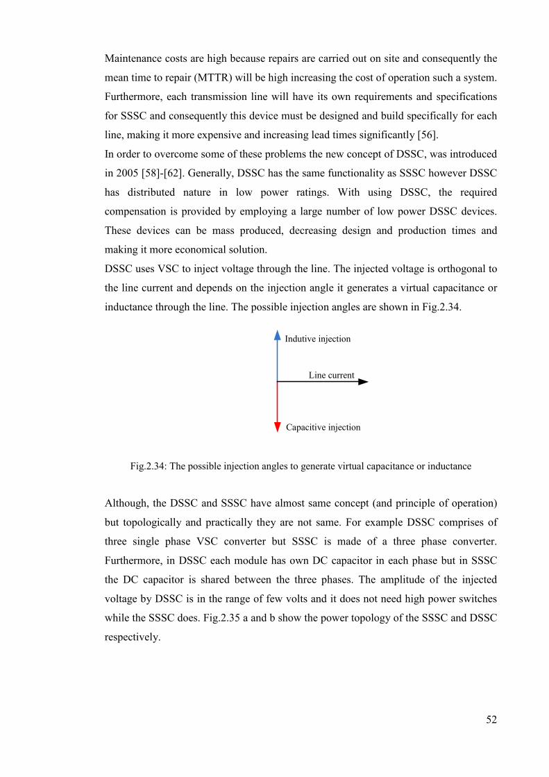
52
Maintenance costs are high because repairs are carried out on site and consequently the
mean time to repair (MTTR) will be high increasing the cost of operation such a system.
Furthermore, each transmission line will have its own requirements and specifications
for SSSC and consequently this device must be designed and build specifically for each
line, making it more expensive and increasing lead times significantly [56].
In order to overcome some of these problems the new concept of DSSC, was introduced
in 2005 [58]-[62]. Generally, DSSC has the same functionality as SSSC however DSSC
has distributed nature in low power ratings. With using DSSC, the required
compensation is provided by employing a large number of low power DSSC devices.
These devices can be mass produced, decreasing design and production times and
making it more economical solution.
DSSC uses VSC to inject voltage through the line. The injected voltage is orthogonal to
the line current and depends on the injection angle it generates a virtual capacitance or
inductance through the line. The possible injection angles are shown in Fig.2.34.
Line current
Capacitive injection
Indutive injection
Fig.2.34: The possible injection angles to generate virtual capacitance or inductance
Although, the DSSC and SSSC have almost same concept (and principle of operation)
but topologically and practically they are not same. For example DSSC comprises of
three single phase VSC converter but SSSC is made of a three phase converter.
Furthermore, in DSSC each module has own DC capacitor in each phase but in SSSC
the DC capacitor is shared between the three phases. The amplitude of the injected
voltage by DSSC is in the range of few volts and it does not need high power switches
while the SSSC does. Fig.2.35 a and b show the power topology of the SSSC and DSSC
respectively.

53
C
GTO
D
GTO
D
GTO
D
GTO
D
GTO
D
GTO
D
+
-
Series connected
transformer
Three phase
power line
a) Power topology of SSSC
b) Three single phase DSSC
Fig.2.35: Power topology of SSSC and DSSC connected to a three phase power system
Each DSSC employs a single phase H-bridge voltage source converter. In this method
(Fig.2.37) a single turn transformer (STT) is used to inject a series voltage which is
orthogonal to the line current [59]. The STT is suspended from the power line and uses
the power line itself as a secondary winding to inject the voltage. For this reason there
are no concerns about voltage insulation as the device is fully isolated with no

54
connection to ground [60]. Another advantage of DSSC is that it provides more reliable
operation as the number of modules provide redundancy in case of failure of even a few
numbers of devices.
In addition, STT within the DSSC is a two part device which can be easily clamped
around the power line then there is no need for the DSSC modules to be repaired on site
as they can easily be disassembled and carried to a repair centre. This will reduce the
cost of maintenance and increase the reliability and availability of the system. DSSC
also has the capability to cope with short circuit currents following a fault in the power
system. The short circuit current passes through the power line itself and just a small
amount of current(which depends on the turn ratio of the single turn transformer) is
induced on the primary side of the STT. This is a challenging problem for SSSC
compensators because the fault current passes through the series transformer and this
can be extremely dangerous for the transformer [60].
Fig.2.36: Distributed Static Series Compensation (DSSC)
DSSC is also more flexible than SSSC. For example, if more power flow control is
deemed necessary, the number of DSSC units can be increased later-on, unlike SSSC,
which once it has been designed and built there is no possibility for further
functionality. SSSC needs customised design and to be manufactured for specific
project however DSSC can be mass produced and later on more modules can be added

55
through the line. A line reactance profile with DSSC is shown in Fig.2.37. This figure
shows that line reactance can be made capacitive or inductive depending on the number
of switched-in DSSC units and the characteristics of their compensation. It also shows
that the change of reactance is achieved in a stepwise fashion and each step can be
positive, for inductive insertion, or negative, for capacitive compensation. Each DSSC
device can be switched on in order to insert some reactance through the line. In the
following figure in each step one DSSC device is switched on. This process can be
continued in order to meet the required compensation.
Fig.2.37: Example line reactance profile
DSSC devices also have low weight and it is therefore possible to suspend them from
the line. In a three phase power system, each phase has its own independent DSSC
module (as shown in Fig.2.38) which operates independently from the each other.
Meaning that different levels of compensation can be injected into each phase which is
an important consideration in low voltage distribution networks where there are
significant levels of load imbalance.

56
Fig.2.38: A distribution line with suspended DSSC through the line
Each DSSC module comprises a STT which provides an electromagnetic connection to
the power system. The STT is connected to an H-bridge converter via a low pass filter
located between the output of the converter and the STT (Fig.2.39).
The low pass filter is employed to eliminate the converter generated high switching
harmonics. The converter itself includes four Insulated Gate Bipolar Transistors
(IGBTs) connected in anti-parallel with four diodes as shown in Fig.2.39. On the DC
side, the converter is connected to a DC link capacitor used to hold the DC voltage at
the required level. The STT transformer is built of two separate parts which can then be
easily clamped around the power line to suspend the whole DSSC module. For this
reason a DSSC unit can be easily assembled and dissembled [61]. All the control and
communication equipment are built inside the module and are supplied internally from
the unit’s power supply fed by the current drawn from the STT.

57
Fig.2.39: Circuit schematic of DSSC
From the power system point of view, the DSSC modules provide a “smart wire” option
for transmission lines allowing for a more flexible and effective power flow control.
DSSC does not contribute towards the active power compensation because it is not
connected to another auxiliary power source. However, it has a huge impact on the
reactive power by significantly compensating it through the line. It has also been argued
that the deployment of DSSC in an electrical network can reduce the environmental
impact of electricity transmission and distribution as it releases some line capacity and
ease congestion issues [62]. In comparison with SSSC, DSSC has the benefit of using
low rated components as the whole device is working at low power and low voltage.
For example, in [63] the DSSC device is rated for only 10 kVA and the injected voltage
is less than 10 volts. This reduces the total cost of manufacturing because components
like IGBT’s and capacitors can be easily and cheaply sourced.
Power flow control using DSSC devices has been attracting some attention during the
past few years [64]. A PSCAD/EMTDC model of DSSC is presented in [65] for
simulation studies and power flow control investigations. A simple three phase model of

58
DSSC is proposed in [66] to be employed in Newton-Raphson power flow studies.
Other DSSC application such as improvement of voltage stability in power systems has
also been proposed [67]. This is achieved by changing the impedance of critical lines in
the electricity network.
2.12 Control of DSSC
The amount of compensation that comes from DSSC can be controlled locally or via a
centralised control system. In both cases, a special control system is required in order to
operate the DSSC device itself. The control system implemented within the device is
responsible for the proper operation of the device only and it receives the set point for
the required injection from the central controller.
In a DSSC, the compensation is achieved from a controlled voltage source converter (H-
bridge converter). However, the converter just tracks the reference signal that comes
from the controller. That shows importance of the employed controller. The generated
reference signal must be synchronised with the AC power system, having the correct
phase angle and amplitude in order to meet the requirements of the compensation. The
compensation percentage can be changed by the control system that is provided by the
network operator, where it is required that the controller be able to cope with the new
parameters. In addition, there may be disturbances or an unbalance within the AC power
system, thus the employed controller in the DSSC must be able to overcome such
issues.
From the control point of view, the DSSC tackles the issues slightly different than the
SSSC. Each phase in the DSSC is independently controlled and therefore, the injected
voltage through each phase could be totally different from the other two phases. While
in the SSSC, generally, balanced three-phase is injected into the power system.
However, the aim is the eventual compensation of the line reactance and control of
power flow in the electrical networks. Different approaches have been used in the SSSC
applications, however some of them cannot be employed in the DSSC because of either
their three-phase nature or they have drawbacks and disadvantages that will be
discussed later in this chapter.
DSSC is a new concept however its principle of operation is same as the SSSC device.
Employed control strategies in the SSSC have been investigated in order to evaluate the
possibility of their employment in the DSSC devices. L.Gyugyi proposed a system
using a controlled VSC to provide a series compensation in the transmission lines. In
this work, the use of a voltage source converter was proposed to adjust the transmission

59
angle between the sending and receiving end buses. Further to this, L. Gyugyi explained
the principle of series compensation with the applied control strategy, in that it is mainly
structured by presenting a 90 degree phase shift between the injected voltage and line
current [62, 2].
The phase shift between the line current and injected voltages has been provided by
different methods suggested in the literature. Some studies are based on the regulation
of the phase angle and amplitude [68], [3]. In this method the angle is derived from the
difference of the DC voltage and the target voltage after passing through a controller
(holding the DC voltage in a desired value is commonly respected by all of the
controllers). The amplitude of the injected voltage is then calculated by using the
required percentage of compensation.
Another method, which is widely used in most of the control strategies, is simply
shifting the line current signal by 90 degrees [35], [69]-[71]. In the control strategies
that are found to be frequently implemented within the literature are using dq
conversion in the control system [35], [68]-[71]. The dq conversion system is used to
convert the three AC voltages or currents to the dq domain and then apply the control
strategy within this domain.
There are two main factors in control of DSSC that must be properly addressed. The
first involves finding the right amplitude of the injected voltage, which is significant to
the extent that it defines the percentage of compensation, or the amount of injected
capacitive or inductive reactance. The second is the phase angle of injected voltage,
which must be orthogonal to the line current phasor in order to guarantee the stable
injection by the device. Moreover, this angle can be controlled so that the injected
voltage is either leading or lagging the line current in order to create inductive or
capacitive reactance.
2.12.1 Control strategy based on dq
In order to calculation phase angle and amplitude of the injected voltage different
methods have been used in the literature review. For example, in [2] and [3], the
amplitude of the injected voltage and its phase angle are calculated separately. The
block diagram of control strategy to generate reference signal in [2] is shown in
Fig.2.40. In this method, the main part of the control is based on the dq conversion. The
Iabc is converted to the Idq and synchronous conversion can be done by the use of a phase
locked loop (PLL). After providing Idq, the amplitude of the line current is calculated as
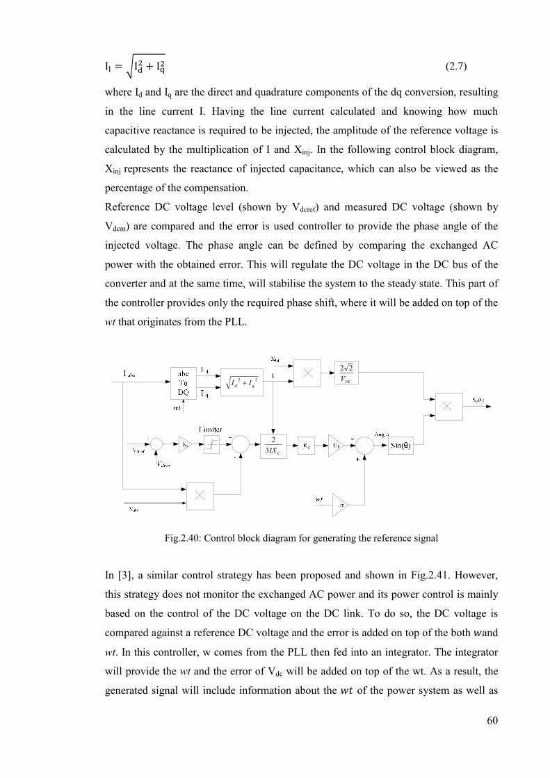
60
I6 = I7% + I9% (2.7)
where Id and Iq are the direct and quadrature components of the dq conversion, resulting
in the line current I. Having the line current calculated and knowing how much
capacitive reactance is required to be injected, the amplitude of the reference voltage is
calculated by the multiplication of I and Xinj. In the following control block diagram,
Xinj represents the reactance of injected capacitance, which can also be viewed as the
percentage of the compensation.
Reference DC voltage level (shown by Vdcref) and measured DC voltage (shown by
Vdcm) are compared and the error is used controller to provide the phase angle of the
injected voltage. The phase angle can be defined by comparing the exchanged AC
power with the obtained error. This will regulate the DC voltage in the DC bus of the
converter and at the same time, will stabilise the system to the steady state. This part of
the controller provides only the required phase shift, where it will be added on top of the
wt that originates from the PLL.
22
qd II + DCV
22
CIX3
2
Fig.2.40: Control block diagram for generating the reference signal
In [3], a similar control strategy has been proposed and shown in Fig.2.41. However,
this strategy does not monitor the exchanged AC power and its power control is mainly
based on the control of the DC voltage on the DC link. To do so, the DC voltage is
compared against a reference DC voltage and the error is added on top of the both :and wt. In this controller, w comes from the PLL then fed into an integrator. The integrator
will provide the wt and the error of Vdc will be added on top of the wt. As a result, the
generated signal will include information about the :; of the power system as well as

61
the error of the DC voltage. It means that the signal is synchron with the system and
tries to eliminate the error within the DC voltage.
The phase angle of injected voltage can be altered in order to provide proper angle of
injection. This is because when the DC voltage in the capacitor is less than the reference
voltage then the error will have non-zero value. Consequently, it will shift the phase
angle, making the exchange of active power possible. The problem with this controller
is that the 90 degree phase difference between the injected voltage and the line current
is not of the utmost importance. The first priority is to keep the DC voltage constant.
While keeping the DC voltage at a constant value can bring stability to the system, the
orthogonal injection is still not guaranteed. This type of controller is partly the same as
the control block diagram as shown in Fig.4.40.
In order to obtain the amplitude of the injected voltage, the dq conversion has been
used, thus bringing up some disadvantages. It must be noted that in both controllers that
are shown in Fig.2.40 and Fig.2.41, the Xinj can be positive and negative. The positive
Xinj represents the capacitive injection, where the aim of the compensation is to reduce
the inductive reactance of the line. The negative Xinj represents the inductive reactance,
whereby injecting such a reactance into the power system results in the total reactance
of the line to increase. The injected voltage in inductive mode has exactly a 180 degree
phase difference with the capacitive injection.
Generally, in both of the discussed controllers, the phase angle of the injected voltage
controls the power exchange of the series compensator, and the amplitude of the
injected voltage determines the percentage of the compensation. These two pieces of
information are obtained from a sinusoidal signal and the generated signal can be fed
into a PWM generator, providing the switching pattern.

62
22
qd II +
dcV
22
Fig.2.41: Block diagram of dq based controller

63
2.12.2 Control strategy based on 90 degree phase shift
In another approach the required phase angle i provided by shifting the phase of the line
current by 90 degrees. This method is simple, as shown in Fig.2.42, and can be executed
by locking to the power system using a PLL. To do so, a PLL must provide the online
and synchronised angular frequency of the system based on the line current information.
To proceed, ±π/2 must be added on top of the phase angle of the line current phasor.
However, the amplitude of the injected voltage can be calculated in different ways. For
example, it can be included in the phase angle of the reference signal and changed in the
DC voltage. Consequently, the DC voltage amplitude can be changed by the amplitude
of the final injected voltage. Alternatively, the amplitude of the reference signal can be
calculated separately and can be multiplied with the reference sinusoidal signal. While
having the amplitude of the reference signal is calculated separately, the DC voltage
level remains unchanged. This can be an advantage in the system design and can reduce
the cost of equipment.
Fig.2.42: Shifting line current
Although this is a simple approach and can even be used in the single phase control,
there are some inherent problems with this method that makes its application practically
difficult. For example, in this approach it is assumed that if a 90 degree phase shift is
introduced between the injected voltage and line current then the injected voltage will
produce pure inductive or capacitive reactance. Consequently, there will be no active
power exchange between the compensator device and power system. However, to
practically in compensate the ohmic and switching losses inside the device, the phase
angle of injected voltage needs to be diverted slightly from 90 degrees. Furthermore, the
losses can vary for the different amplitude of the injected voltage, allowing the required
amount of diversion of phase angle from 90 degree to also vary. As a result, the
diversion must dynamically track the losses and try to compensate it. For this reason,
having only a 90 degree phase shift within the phasor of the line current and
establishing the injected voltage based on the shifted signal cannot be 100% accurate.

64
However, in the literature review this method is widely used in the implemented control
strategies of the SSSC and DSSC [72]. For example, Fig.2.43 shows a control block
diagram that is implemented in [35]. In this block diagram, Id and Iq, the two orthogonal
components of line current are calculated using the dq conversion and provide the
angular frequency of the power system by PLL. The phase angle is obtained in (2.8) and
the magnitude of the current can be calculated from (2.7).
θ = tan?(AB) (2.8)
The calculated phase angle is used as a base angle and synchronises the injected voltage
with the power system voltage phasor. However, in order to have a 90 degree phase
shift, as can be clearly observed in the control block diagram, a value of –π/2 is added
on top of the obtained phase angle. The added angle does not consider any losses within
the SSSC device, which can threaten the steady state stability of the system.
In the block diagram shown in Fig.2.43, similar to the control systems shown in
Fig.2.44, the amount of the injected voltage is calculated based on the amplitude of the
line current and the required injected reactance. In control system shown in Fig.2.43, Xq
represents the required injected reactance and is multiplied with I, which is calculated
using equation (4.6). The resultant signal, after passing through the gain, represents the
reference signal for the required DC voltage in the DC link. It means that DC voltage is
different for different amount of required reactance injections and the amplitude of the
voltage varies based on the value of injected reactance. The signal is compared with the
measured DC voltage and the error is added on top of the injected phase angle. This will
help the system to maintain the DC voltage for the desired value as by changing the
phase angle the system will be able to absorb or inject active power into the system.
The DC voltage can then be regulated and the amplitude of the injected voltage will be
adjusted. However, the DC voltage needs to be changed by a different level of
compensation. The capacitive or inductive injection by the system will be defined by
changing the sign of the added value such that it becomes –π/2. The system continues
by changing the sign of the error, which comes from the deduction of the measured
voltage from the reference DC voltage. Finally, the generated phase angle is fed into a
sine function to provide the sinusoidal signal. This signal is used by a PWM generator
to provide the required switching pattern for the IGBTs.

65
invK
1
2
π−
Fig.2.43: Line Current shifted ± 90 degree
A similar approach has been used in [69], where the dq conversion is used to obtain the
angle and amplitude. However, in [70]-[71], adding a 90 degree phase has been
implemented as shown in Fig.2.44 with slightly differences. In this control strategy, the
feedback of the injected voltage is converted to Vd and Vq.
Orthogonal element of the voltage is used to calculate XS, which is the compensated
reactance. The parameter XS is then compared with the reference reactance and the
resultant error is fed into a PI controller. The error provides the fine tuning angle and
the angle must be added on top of the wt (representing the angular frequency of the
power system) which comes from a PLL. However, a value of ±π/2 must be added on
top of the angle coming from PLL (θ) and the error angle (∆α) to provide the inductive
or capacitive injection.

66
Fig.2.44: Control block diagram of SSSC using 90 degree phase shift
In this strategy, the losses through the filter and even the converter itself are not
considered, where the practical experiments can result in instability. To avoid such a
problem, there must be another factor which is added on top of the final calculated angle
that provides an active power absorption possibility by the converter in order to
compensate for the losses.
2.13 Drawbacks with dq based controllers
The dq conversion and its equations have been explained in Appendix A. Using a dq
control within a power system can raise some problems when it is unbalanced or
harmonically polluted. In unbalance power systems dq components are oscillatory and
zero sequence is not zero any more. The oscillatory dq components can cause
malfunction of controllers and it will lead to failure of the converter. Furthermore, a dq
control can lose the stability in connection with power system with low short circuit
levels. The issue is, to a large extent, related to the phase-locked loop and its ability to
stay in synchronism with the PCC voltage. As the power changes then the PCC voltage
angle changes too. This requires the PLL to re-establish its lock. If the system is weak,
this impact is more significant. The situation escalates if we take the resistive part of the
system impedance into account (i.e. relatively low X/R ratio) [73].
2.13.1 dq conversion in balanced three-phase system
In all the equations which are explaining the dq conversions in the appendix A, the
power system is assumed to be balanced. Otherwise, the conversion can be incorrect

67
and results in an inaccurate calculation. For example, power systems can be unbalanced
if the amplitudes of the voltages in the three-phases are different or if the phase angles
between the phases are not identical.
A dq conversion of a balanced three-phase voltage is shown in Fig.2.45. The amplitude
of the abc axes is one per unit and the dq axes is also shown with a one per unit
amplitude. The amplitude of “q” and “o” are zero and it shows that the applied three-
phase system is a balanced system.
Fig.2.45: dq conversion of a balanced three-phase system
In an ideal case the phase angle between the “d” and “q” components must be 90
degrees. Their amplitude must be also completely independent from each other. This
figure shows that with a balanced three-phase system, the “d” and “q” components will
be identical. Even if the resultant “d” and “q” components are fed into a dq to abc
converter, the resultant abc waveforms will be the same as the original. However, in all
of the conversions, the PLL plays a very important role and any failure within the PLL
will endanger the synchronicity of the power system.
In the case of an unbalanced three-phase system, the amplitude of the “d” and “q”
components can be different. At the same time the phase angle between them can also
be different from the previous 90 degree constraint.
Sec 0.100 0.120 0.140 0.160 0.180
-1.00
1.00
PU
a b c
-0.20
1.20
PU
d q o

68
2.13.2 dq conversion in unbalanced three wire three-phase system
A three wire three-phase system can be unbalanced because of the different amplitude
of voltages in each phase and/or different phase angles between them. The definition of
percentage of unbalance is explained in the appendix A. If the phase to phase voltages
for the three phases in a three-phase system are 1.2p.u, 0.8p.u and 1p.u, then the average
voltage can be calculated as
VEFG = ?.%#?#I.JK =1 (2.8)
and then the Max ∆V will be
∆V=1-0.8=0.2.
The percentage of unbalance can be calculated using equation (A.16) as follow:
PercentageofUnbalance = ?II∗I.%? = 20% (2.9)
The dq conversion of unbalance three phase three wire AC system with an unbalance of
20% is shown in Fig.2.46.
Fig.2.46: abc to dq conversion of unbalance three-phase system
It can be clearly observed that in the dq conversion of the unbalanced system, the
amplitude of the “d” and “q” components are different and oscillatory.
Having an unbalanced three-phase system converted to dq and again converted from dq
to abc is shown in Fig.2.47. It can be clearly observed that the final conversion to abc is
unbalanced, which can increase the disturbance in the AC system. In SSSC applications,
when the dq conversion is applied to an unbalanced AC system in order to provide the
dq components, the compensation cannot be same in the three-phases. This is because
the provided dq components can be inaccurate and the phase angle between them can be
Sec 0.1500 0.1550 0.1600 0.1650 0.1700 0.1750 0.1800 0.1850 0.1900
-1.50 -1.00 -0.50 0.00 0.50 1.00 1.50
PU
a b c
-0.40
1.40
PU
d q o

69
different from the 90 degree requisite. Consequently, after applying the control strategy,
the converted signals to abc components will carry incorrect information.
Fig.2.47: Conversion from abc to dq and from dq to abc in an unbalance three-phase system
In another unbalanced three-phase system with identical voltage amplitudes but
different phase angles of 100, 110 and 150 degrees, the results of dq conversion can be
far from the ideal case. The conversion of abc to dq is shown in Fig.2.48, where it can
be observed that when there is a difference in the phase angle in the three-phase system,
the amplitude of the “d” and “q” components will be different and oscillatory. In order
to observe clearly the detail of the dqo, Fig.2.48 has been spanned through the time axis
and it is shown in Fig.2.49.
Fig.2.48: abc to dq conversion in an unbalanced system
Sec 0.0500 0.0550 0.0600 0.0650 0.0700 0.0750 0.0800 0.0850 0.0900
-1.50 -1.00 -0.50 0.00 0.50 1.00 1.50
PU
a b c
-1.50 -1.00 -0.50 0.00 0.50 1.00 1.50
PU
a1 b1 c1
Sec 0.100 0.150 0.200 0.250 0.300 0.350 0.400 0.450 0.500
-1.50 -1.00 -0.50 0.00 0.50 1.00 1.50
PU
a b c
-0.20
1.20
PU
d q o

70
Fig.2.49: abc to dq conversion in an unbalanced system spanned through the time axis
With the intention of investigating dq conversion in the presence of a difference in the
angle between the three-phases, the angle between the “d” and “q” components is
plotted in Fig.2.50.This figure shows that the angle is approximately 107 degrees, which
shows a deviation from the 90 degree. It also means that the dq components are not
orthogonal to each other, which can be problematic. For example, in control strategies
that establishes all of the calculations related to the active power on the “d” component
where all of the calculations pertaining to the reactive power are based on the “q”
components, the 90 degree phase angle between the dq components are required in
order to control active power and reactive power independently. Consequently a
malfunction of a control system through the missing of such a requirement can be
expected.
For instance, if an unbalanced system is converted to dq and simply converted back to
abc, the resultant waveform will also become unbalanced. This is shown in the Fig.2.51.
It can be seen that the a1b1c1-, which is converted from dq to abc-, is same as the abc. It
means that in the case of the application of dq conversion in SSSC controllers, the
injected voltage itself is not balanced and can result in a different amount of
compensation through the line.
Sec 0.050 0.060 0.070 0.080 0.090
-1.50 -1.00 -0.50 0.00 0.50 1.00 1.50
PU
a b c
-0.20
1.20
PU
d q o
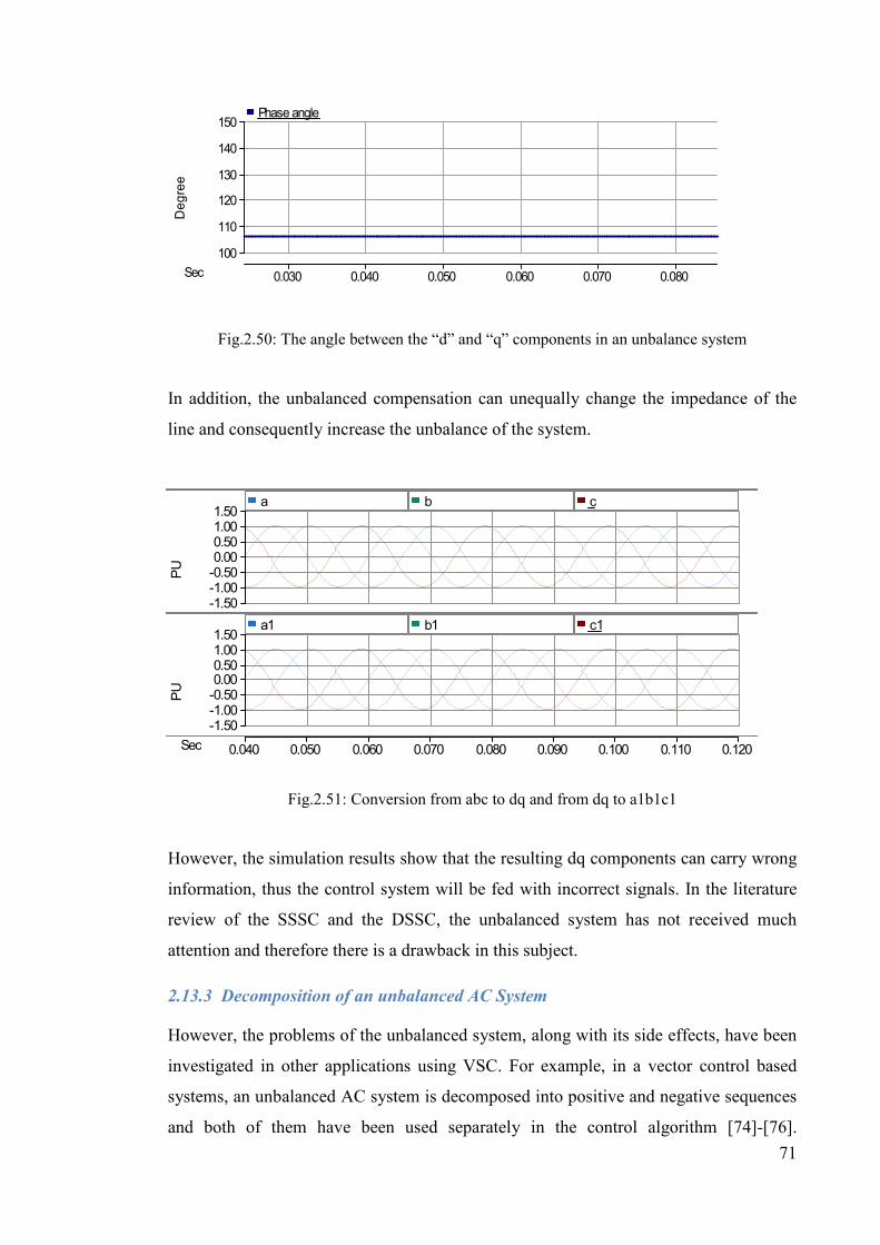
71
Fig.2.50: The angle between the “d” and “q” components in an unbalance system
In addition, the unbalanced compensation can unequally change the impedance of the
line and consequently increase the unbalance of the system.
Fig.2.51: Conversion from abc to dq and from dq to a1b1c1
However, the simulation results show that the resulting dq components can carry wrong
information, thus the control system will be fed with incorrect signals. In the literature
review of the SSSC and the DSSC, the unbalanced system has not received much
attention and therefore there is a drawback in this subject.
2.13.3 Decomposition of an unbalanced AC System
However, the problems of the unbalanced system, along with its side effects, have been
investigated in other applications using VSC. For example, in a vector control based
systems, an unbalanced AC system is decomposed into positive and negative sequences
and both of them have been used separately in the control algorithm [74]-[76].
Sec 0.030 0.040 0.050 0.060 0.070 0.080 ...
... ...
100
110
120
130
140
150
Degree
Phase angle
Sec 0.040 0.050 0.060 0.070 0.080 0.090 0.100 0.110 0.120
-1.50 -1.00 -0.50 0.00 0.50 1.00 1.50
PU
a b c
-1.50 -1.00 -0.50 0.00 0.50 1.00 1.50
PU
a1 b1 c1
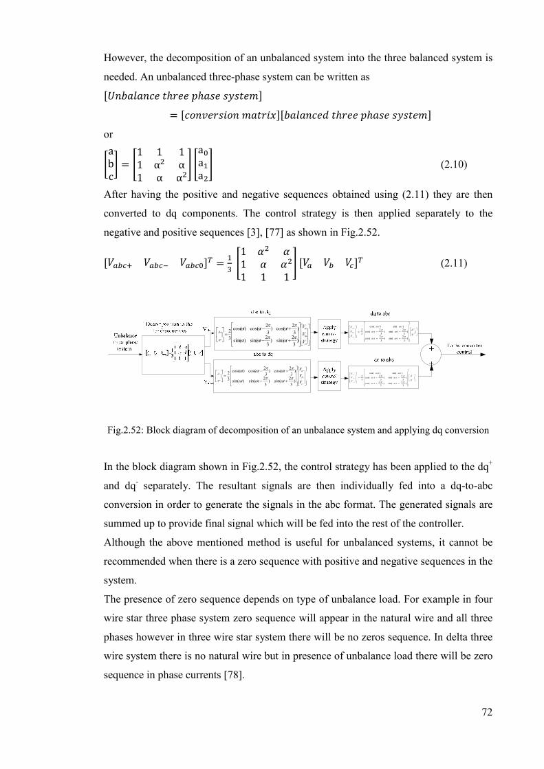
72
However, the decomposition of an unbalanced system into the three balanced system is
needed. An unbalanced three-phase system can be written as VWXYZ[ZX\];ℎ_]]`ℎZa]aba;]cd= V\eXf]_ageXcZ;_ghdVYZ[ZX\]i;ℎ_]]`ℎZa]aba;]cd or
jabck = l1 1 11 α% α1 α α%o laIa?a%o (2.10)
After having the positive and negative sequences obtained using (2.11) they are then
converted to dq components. The control strategy is then applied separately to the
negative and positive sequences [3], [77] as shown in Fig.2.52.
V(pqr# (pqr (pqrIds = ?K l1 2% 21 2 2%1 1 1 o V(p (q (rds (2.11)
+−
+−=
+
+
+
+
+
c
b
a
q
d
V
V
V
ttt
ttt
)3
2sin()
3
2sin()sin(
)3
2cos()
3
2cos()cos(
3
2
πω
πωω
πω
πωω
+−
+−=
−
−
−
−
−
c
b
a
q
d
V
V
V
ttt
ttt
)3
2sin()
3
2sin()sin(
)3
2cos()
3
2cos()cos(
3
2
πω
πωω
πω
πωω
++
−−=
+
+
+
+
+
q
d
tt
tt
tt
V
V
V
c
b
a
)3
2sin()
3
2cos(
)3
2sin()
3
2cos(
)sin()cos(
3
2
πω
πω
πω
πω
ωω
++
−−=
−
−
−
−
−
q
d
tt
tt
tt
V
V
V
c
b
a
)3
2sin()
3
2cos(
)3
2sin()
3
2cos(
)sin()cos(
3
2
πω
πω
πω
πω
ωω
Fig.2.52: Block diagram of decomposition of an unbalance system and applying dq conversion
In the block diagram shown in Fig.2.52, the control strategy has been applied to the dq+
and dq- separately. The resultant signals are then individually fed into a dq-to-abc
conversion in order to generate the signals in the abc format. The generated signals are
summed up to provide final signal which will be fed into the rest of the controller.
Although the above mentioned method is useful for unbalanced systems, it cannot be
recommended when there is a zero sequence with positive and negative sequences in the
system.
The presence of zero sequence depends on type of unbalance load. For example in four
wire star three phase system zero sequence will appear in the natural wire and all three
phases however in three wire star system there will be no zeros sequence. In delta three
wire system there is no natural wire but in presence of unbalance load there will be zero
sequence in phase currents [78].

73
If there is zero sequence then it will not be compensated in the approach shown in
Fig.2.52 and as such, it can disturb the final signal. For example, an unbalanced signal
that is a combination of 0.85 p.u positive sequence, 0.1 p.u negative sequence and 0.05
p.u zero sequence has been investigated. The resultant final signal, as shown in
Fig.2.53, in abc format is the conversion of the combination of the positive and negative
sequences. However, the amplitude of the waveform shows that it is less than 1p.u, in
fact it is actually 0.95 p.u. It can be argued that the contribution of the zero sequence,
which is equal to 0.05 p.u, is missing and for this reason, the final value of the
converted signal is less than 1 p.u. One of the advantages of this method is that the final
converted waveform, which includes the positive and negative sequences, is in phase
with the positive sequences and rotates synchronously with the positive sequences. With
the intention of comparing the phase angle between these two signals, the positive
sequence and the final converted signal are plotted in Fig.2.54.
Fig.2.53: Conversion of combination of positive and negative signal
Sec 0.000 0.020 0.040 0.060 ...
... ...
-1.00 -0.90 -0.80 -0.70 -0.60 -0.50 -0.40 -0.30 -0.20 -0.10 0.00 0.10 0.20 0.30 0.40 0.50 0.60 0.70 0.80 0.90 1.00
PU
apn bpn cpn

74
Fig.2.54: Positive sequence and final converted waveform
In the above figure the synchronicity among the positive sequences and the final
converted waveform is obvious, but for the purpose of clarity, the phase angle
difference between them is plotted in degree in Fig.2.55. This plot shows that the phase
difference between them is absolutely zero.
Fig.2.55:Phase angle difference between the positive sequences and the final converted waveform
The dq conversion clearly has the advantage of synchronisation with the final waveform
with the positive sequence. However, this advantage can easily disappear with a
malfunction of the PLL. The reason for this is based on the equations (A.11) and (A.13),
where the synchronisation is ensured by providing an accurate value of wt, and the
value wt is updated constantly by PLL. At the same time, the proper operation of the
Sec 0.0000 0.0050 0.0100 0.0150 0.0200 0.0250 0.0300 0.0350 0.0400 0.0450 0.0500 0.0550 0.0600 ...
... ...
-1.00
1.00
PU
a b c
-1.00
1.00
PU
apn bpn cpn
Sec 0.00 0.10 0.20 0.30 0.40 0.50 ...
... ...
-10.0
-8.0
-6.0
-4.0
-2.0
0.0
2.0
4.0
6.0
8.0
10.0
Degree
Angle

75
PLL can be endangered by various issues. For example, in harmonically polluted
electrical networks, tracking the correct frequency can be an issue. Furthermore, in
weak AC electrical networks, switching events or even a load rejection can cause the
PLL to lose synchronicity because of a SCL. Moreover, the PLL itself has a PI
controller as shown in Fig.2.56 [79], [80] which is tuneable based on the value of its
proportional or integrator gain, such that the output error can be minimised.
Fig.2.56: Block diagram of the phase locked loop (PLL)
The tuning of the PLL for a SCL of an AC system is one of the key parameters which
must be considered [81]. However, the SCL of a power network can be changed by
some events such as tripping a line or coming in or out of a power plant. Practically, the
mentioned events usually happen in the electrical power networks and when the change
of a SCL is unavoidable. On the other hand, a PLL that is tuned for a system with a high
short circuit level may not work or may not have the same performance for a system
with a low SCL. Subsequently, any change in the SCL may result in an out of tune PLL,
which will require retuning for updated system parameters.
Based on the aforementioned problems regarding the operation of a PLL in connection
with an AC system, it can be argued that a PLL can reduce the reliability of the dq
conversion. In this study and in the literature review, it has been noted that the dq
conversion has been used in most of the controllers in the literature review. However,
synchronicity is a key requirement of a control system that must be met otherwise the
controller will lose the orthogonal injection of series voltage.
In addition the amplitude of the “d” and “q” components must be accurate, otherwise a
pure reactive power injection that is mainly based on the “q” component can be mixed
with the active power injection. This can lead to instability and finally the DC voltage
will collapse. Furthermore, the phase angle between the “d” and “q” components can be
diverted from the 90 degree in the presence of unbalanced power systems and
consequently this will disturb the assumption of having two orthogonal components in

76
the dq domain. It is worth mentioning that having two “d” and “q” components that are
orthogonal is a key requirement to provide an independent control of active and reactive
power. This future is very dominant when the dq conversion is used by a vector control
through the control system.
In order to avoid employment of dq conversion within the control of either DSSC, it is
required that a controller to be independent from the unbalance in the system. A novel
approach based on the single phase control rather than three-phase will be introduced in
chapter 4.
2.14 Summery
Line reactance is a key parameter in determining the available transmission capacity of
a power line. Also, it is an important factor in the voltage stability and power system
stability enhancement. To achieve these, line reactance can be altered and one of the
alteration methods is the use of series compensation techniques. Series compensation
can be achieved in different ways. Traditionally, fixed capacitors are employed in series
with transmission lines in order to reduce the effects of line inductance. However, fixed
capacitors can only introduce capacitive compensation and are not able to provide an
inductive reactance which may be required in a power flow control problem. There are
also other issues associated with the application of fixed capacitor in an electrical
network. Fixed capacitors can initiate a SSR phenomenon and the resultant resonance
can damage the network.
For this reason, the use of series compensation devices utilising power electronics
switches was established. A number of such schemes, such as TSSC and TCSC devices,
were reviewed in this chapter and their principles of operation outlined. The use of
voltage source converters as series compensation devices in SSSC schemes has also
been described. The many operational advantages of SSSC circuits have been discussed
as well as their drawbacks in terms of their high costs and reliability issues associated
with the flow of short circuit currents.
DSSC was introduced as a concept to overcome some of these problems. This device is
a single phase device and it is comprised of a VSC converter and STT. It is suspended
from the power lines and it can be easily assembled and disassembled. It has low power
rating in comparison with the power electronics based series compensators.
Concept of control of DSSC is discussed followed by an explanation of the commonly
used controllers in the literature review. Two different methods of using 90° phase shift
77
and dq conversion based control strategy have been identified. Both methods have been
explained and their advantages and disadvantages were discussed.
In 90° phase shift method the injected voltage can be built based on the shifting 90°
phase of the line current. This will provide a signal that is orthogonal to the line current.
However, because of the losses, it can cause instability in the system. To avoid
instability, the injected phase angle must be slightly different from the 90°. Although
the adjustment of the phase angle in order to be diverted slightly from 90° degree to
compensate the internal losses inside the DSSC must occur frequently, otherwise the
operation of device will not be stable.
In dq based controllers use of PLL is necessary and in most of the phase control
strategies applied here, the dq conversion has been used. Nevertheless, the dq
conversion in the presence of unbalanced system can result in inaccurate dq components
in terms of amplitude or the angles in between. Furthermore, an unbalanced system can
be decomposed into positive, negative and zero sequences. The negative sequence can
be compensated by its conversion to the dq domain, applying the same control strategy
as that used for the positive sequence. However, the compensation can only be obtained
in systems where their unbalance limited to a very low percentage, less than 5% for
example. Additionally, in this approach only a negative sequence is being compensated
and the zero sequence remains uncompensated.
To overcome the investigated control problems, there is a requirement for a controller to
operate as a single phase controller and adjust the angle automatically.

78
3 Applications of DSSC in distribution networks
In this thesis, DSSC is proposed as a Distributed FACTS (D-FACTS) device in 11kV
electrical power distribution networks. The proposed approach is presented in Fig.3.1.
In this figure, an 11 kV overhead line distribution feeder is being fed from a distribution
substation and is supplying a residential and industrial load.The aim of application of
DSSC in the distribution network is to dynamically compensate line reactance through
the power line. By decreasing or increasing the line reactance it is possible to push away
current from or pull into a specific line. In addition DSSC can help to increase the ATC
of the compensated feeder. This is a very valuable achievement in the distribution
networks because the rate of increasing demand for the consumption of electricity and
consequently its generation is high.
Fig.3.1: Application of DSSC in electrical distribution networks
However, expansion of distribution utilities has not received much attention. Extra
tension is applied to the distribution networks by direct connection of the renewable
energy resources such as wind farm and solar panels. For this reason application of
DSSC in the distribution utilities can release the capacity of distribution lines, hence
provide capability of enhancing the distribution networks reliability.
Usually distribution feeders supply loads using radial topology. The drawback of this
arrangement is that all loads will be cutout when a trip occurs. Such interruption in
these feeders is not acceptable, therefore DSSC can be a solution for these networks.
DSSC suspends from the power line through STT, so the line current does not pass

79
through the DSSC directly. It means that it is not in series with the line directly and in
the case of failure it can be easily bypassed without interrupting the power flow in the
power line. By passing one DSSC device will not have a big effect on the compensation
because other DSSC device are still in order and they can continue providing
compensation.
In this study, the application of DSSC in the distribution networks and the consequent
side effects has been investigated. Further to that the main body of research is focused
on the control of DSSC itself (control of voltage source H-bridge converter).
3.1 Applications of DSSC in the distribution networks
DSSC has distributed nature and its application through the distribution feeders can
make the power lines to act like a smart wire. This means that injecting proper voltage
(with controlled amplitude and phase angle) in series through the line can improve
different parameters of the power system. For example DSSC can be employed to help
load flow control in the networks. It can mitigate congestion in a particular line or it can
divert the load current in other alternative corridors. In another application it can be
used as a voltage profile improver. These applications have been investigated and are
explained in the following subsections. However, line resistance in the distribution
networks is higher and proper operation of the DSSC in distribution networks must be
investigated.
3.1.1 Effect of line resistance on the control of DSSC
Employed controller within a DSSC provides a reference signal for the converter to
inject a voltage for line reactance alteration purpose. Alteration of line reactance by
DSSC can affect the transmission capability of the line both by increasing or decreasing
the transmitted power. It depends on the X/R ratio of the uncompensated line and for
low ratios compensation can reduce the transmission capability of the line.
Transmitted power (including active power and reactive power) between two buses in a
power system shown in Fig.3.2 can be calculated using equation (3.1).
Fig.3.2: Two bus AC power system

80
S = Vu v uuw#x y∗ (3.1)
Where VS and Vr are the sending end and receiving voltages and RS, XL are representing
the resistance and reactance of the line. Vs and Vr can be substituted with their
amplitude and angle, then (3.1) can be rewritten in equation (3.2).
S = Gz(|z|~)~w (3.2)
Using Euler formula represented in (3.3) and substituting equation (3.4) the complex
power is recalculated in (3.5). e = cos α + j sin α (3.3) δ = θ? − θ% (3.4)
S = w w~# w~# ~EFGG+ j ~(w )w~# ~wGFGG
(3.5)
assuming bus voltages in both ends are 1p.u then Vs will be equal to Vr and with
substituting this assumption in (3.5) active power and reactive power is calculated in
(3.6) and (3.7) respectively.
P = ~w~# ~ VX sin δ − R(1 − cos δ)d (3.6)
Q = ~w~# ~ VR sin δ + X(1 − cos δ)d (3.7)
in long lines w is negligible and by substituting this in equations (3.6) and (3.7) active
and reactive power equations are written in (3.8) and (3.9).
P = ~ w~# ~ (3.8)
Q = ~ (?)w~# ~ (3.9)
Practically, power lines have some ohmic resistance along with reactance and with
considering nonzero value for Rs the transmitted active power is written in (3.10) by
rearranging (3.8) and substituting RS with R and XL with X.
P = (w) ~ w(?# ~) (3.10)
Then transmitted power versus δ(phase angle difference between voltages at the both ends of line) will be affected by X/R ratio of line. This is shown by plotting P using
equation (3.6) for different values of X/R ratio in Fig.3.3.

81
Fig.3.3: Effect of X/R ratio on the transmitted power
This plot clearly shows that if the X/R ratio goes high the ATC will be high and vice
versa. In addition with low X/R ratio peak value of power occurs in lower angles which
can endanger stability of the system. For example in Fig.3.3 peak value of power for
X/R ratios of 20 and 10 take place in almost 87° however for lower ratios such as 1 it
happens in 45.8°.
In order to investigate the effect of X/R ratio on the transmitted power a two bus AC
power system as shown in Fig.3.4 has been utilized and simulated in PSCAD.
Fig.3.4: Compensated AC power system
In power lines with higher X/R ratio normally capacitive compensation is required to
reduce the effect of inductive reactance. However the reduction of X must be in a way
to not endanger the stability of power system.
In compensation using DSSC the transmitted power between the sending end and
receiving end buses becomes function of injected voltage and it is obtained in (3.11) [1],
[55].
P = ~ − (~)
(3.11)
0 45.8 87.7 174 1800
0.1
0.2
0.3
0.4
0.5
0.6
0.7
0.8
0.9
1
Angle [Degree]
Power [p.u]
X/R=20
X/R=10
X/R=5
X/R=2X/R=1
X/R=0.5

82
where Pcom is the contribution of compensation provided by injected voltage VInj. In
(3.11) the following assumption has been used (¡ = (¢ = ( (3.12)
where Vs and Vr are the bus voltages. By substituting Vr and Vs with V in (3.11) the
new equation is obtained in (3.13).
P = − (~) × ¤ (~)(¥¦¥~¥ )~¥¥~(~)§)¡¨*)©ª)«¬® (3.13)
The parameter XL is the line reactance and δ is the phase angle between Vs and Vr. The
effective inductance will be changed by injecting capacitive or inductive reactance
through the line by using DSSC between the two buses. As a result, the transmitted
power will be changed, as shown in Fig.3.9.
Fig.3.5: Change of transmitted power against transmission angle
However, by compensating the line reactance then the phase angle of voltages at the
receiving end buses will also change. For this reason, the DSSC can also be employed
as a distributed static phase shifter (DSPS) through the networks. Theoretically phase

83
angle of 90° and above can lead to instability in the power system due to interaction
with governor of generators [85].
3.1.2 Calculation of required numbers of DSSC
The provided compensation by DSSC is calculated in equation (3.14).
X = ¯°¯± (3.14)
where Xinj is the provided reactance and Vinj is the injected series voltage by each DSSC
module and line current is represented by Iline in this equation. Assuming Kc percentage
of the line reactance, Xl, is required to be compensated and it can be calculated as
follow X7 = KX6 (3.15)
where Xcd is demanded compensation reactance.
In the other hand each DSSC devices has a limited capability in providing
compensation, Xinj, through the line. The restriction is defined mainly by the rating of
the components and the voltage source converter within the DSSC device. However,
number of required modules is calculated in equation (3.16).
n = ²B¯ (3.16)
where n is the required number of DSSC devices through the line. For example, in a
power line (as shown in Fig.3.2) with 20 miles length, total reactance of 6.25Ω and
resistance of 2.86Ω for FeAl234 conductor can be obtained from Table 3.1. This table
shows typical line parameters in an 11kV distribution system. Assuming a
compensation of 20% is required then DSSC modules must provide 1.25Ω capacitive
reactance. Each module can be designed to inject 10V (depends on the design of DSSC
the injected voltage can be customized to different values) orthogonal with line current
of 345A then provided capacitive reactance by the module will be 0.02898Ω. By
dividing required capacitive reactance, 3.98Ω, with provided reactance of 0.057Ω the
number of DSSC modules will be 43. Summary of parameters and corresponding values
within the explained example is presented by Table 3.2 [84].

84
ACSR
Type
Cross section Current capacity R L
FeAl234 234mm2 345A 0.143Ω/mile 0.996mH/mile
Chickadee 1118mm2 575A 0.2281Ω/mile 1.19mH/mile
Table 3.1: Typical bare conductors in an 11kV distribution system
Parameter Value
Reactance of the line 6.25Ω
Resistance of the line 2.86Ω
Percentage of compensation 20%
Line current 345A
Injected voltage 10V
Injected reactance 1.25Ω
Required number of DSSC devices 43
Table 3.2: Summary of parameters and corresponding values
3.2 Load flow control using DSSC
In order to investigate capability of DSSC in controlling load flow in electrical
distribution networks a power system including two parallel lines has been considered.
The power system is shown in Fig.3.10 and the system parameters are tabulated in
Table 3.3. Line1 is equipped with 20 DSSC devices and its reactance can be
compensated. Current capacity of line1 is higher than line2 and the aim is to divert
current from line2 to line1 using DSSC.
Line number
Conductor type Line resistance
Line reactance
Compensation Line current capacity
1 ACSR (Chickadee)
2.368Ω 5.175Ω Yes 575A
2 ACSR (FeAl234)
2.86Ω 6.25Ω No 345A
Table 3.3: System parameters for two parallel lines

85
Fig.3.6: Compensation of two parallel lines
Line1current in at different level of compensation is plotted in Fig. 3.11. In this figure
current in line1 is shown with blue line and in line2 is shown with green. First time
interval belongs to the system with no compensation and the second belongs to a system
with 20 % compensation provided by DSSC modules in line1. In this time interval as a
result of compensation, current in line1 increases because of less line impedance and in
the line2 the current decreases. Third time interval of the plot show the result of further
compensation and corresponding changes of current in the lines. This is a very useful
feature of application DSSC in the distribution networks which allows the operator to
divert current partially from one line to another.
Fig.3.7: Phase current with different level of compensation
DSSC not only can push current into the compensated line but also it can pull away
current from the compensated line. This can be achieved by injecting inductive current
through a line. Fig.3.12 shows current is pulled away from line1 and pushed into line2.
In this figure at first there is no voltage injection but afterward with injection of 20 %
inductive reactance current in line1 goes down and in the same time it goes up in the
line2. Moreover with increasing the injection of inductance furthermore the line current
in line1 decreased further and it is increased in line2.
Sec 0.00 0.20 0.40 0.60 0.80 1.00 1.20 1.40 1.60 1.80 2.00 2.20 2.40 2.60 2.80 3.00 ...
... ...
0
100
200
300
400
500
Current [A]
IA1 IA2

86
Fig.3.8: rms value of lines current in presence of inductive injection
3.3 Voltage profile improvement using DSSC
In the distribution feeders the loads connected to line in different distances from the
distribution substation. Consequently the impedances of the lines are different and then
the amount of voltage drop across the lines will be different. Actually, the voltage drop
increases when the distance increases. The voltage drop is a combination of the drop
produced by the ohmic resistance of the wire and its inductive reactance. Because the
inductive reactance can be compensated by using DSSC [88], therefore this opens a new
application for the DSSC, which is proposed in this study to improve voltage profile in
the power distribution networks and compensate the voltage drop which comes from the
inductive resistance of the line.
The distributed nature of DSSC units facilitates their independent operation even with
the reconfiguration of the network. Generally, the overhead line distribution networks
are more vulnerable to short faults but the DSSC modules are immune against the
consequence of flowing the short circuit currents. This is because in the case of a short
circuit fault in the power system, a very small amount of current will be transferred to
the power electronics side of the DSSC device, which is connected in the secondary side
of the single turn transformer with turn ratio of, let say, 1:100. The mentioned feature
nominates the DSSC as a reliable solution in reactive power compensation in the
distribution feeders.
In this application the DSSC modules are connected to the feeder in series as shown in
Time [s] 0.00 0.50 1.00 1.50 2.00 2.50 3.00 3.50 4.00 ...
... ...
0
50
100
150
200
250
300
350
400
450
Current [A]
IA1 IA2

87
Fig.3.13 in order to compensate the reactive consumption of the line itself. Fig.3.14
shows part of a loop distribution network with DSSC devices and lumped loads along
the length of the line. The loads through the feeder can be supplied from both
substations A and B. However, conventionally in the distribution feeder in order to
increase the voltage at the end of feeder some fixed capacitors have been used.
However, with the reconfiguration of the network topology the voltage at the end of
feeder (which is now the begging of the feeder) can be high enough and then there is no
need to have the capacitors to increase the voltage. In that situation the application of
fixed capacitors can be problematic. In contrast to that, the application of DSSC
modules is independent from the reconfiguration of topology of the network because it
can provide compensation through the line rather than in one point of the feeder.
Fig.3.9: 11kV loop distribution network including DSSC devices
Each DSSC module behaves like voltages source through the line. It works based on
injecting capacitive voltage in order to eliminate the effect of line reactance. Fig.3.14
show the model of feeder equipped with the DSSC modules. In this model Ri and Li
(i=1, n) are the resistance and inductance of the section of the line which are located
between two DSSC modules and the DSSC models are represented by the voltage
sources.
Fig.3.10: The model of feeder equipped with the DSSC module
Considering one segment of the line in Fig.3.14, the voltage drop in that section can be
calculated as follow:
Vdrop = Rn I + jXn I + Vinjn (3.17)
where Vdrop is the series voltage drop across the segment, I is the current through the
feeder and Vinjn is the voltage injected by the DSSC module number n. As Vinjn is
orthogonal with the line current, it can be expressed as:

88
Vinjn = (±jX’nI) (3.18)
where X’n is the effective injected reactance. It must be noted that since X’n is not a
physical reactance then it cannot affect the system impedance at frequencies other than
fundamental frequency. For this reason it can contribute toward amplifying or
mitigating the amplitude of the harmonics through the line and it cannot initiate an
oscillation through the system.
Furthermore, in the presence of an inductive load, the line current can be expressed as
follow:
Il = IP + jIQ (3.19)
Substituting (3.18) into (3.17), the Vdrop can be calculated as follow:
ldrop IXXRV 2)'(2 ±+= (3.20)
From the above equation Vdrop can be decreased or increased (based on the polarity of
X’ which depends on whether the injected voltage lags or leads the line current)
allowing the line voltage profile to be controlled. In the distribution networks resistance
of the line is bigger than reactance however manipulating of reactance still will change
voltage profile. The application of DSSC not only alters the voltage drop across the line
but also decreases or increases the inductive reactive power flow through the line. This
is demonstrated by the following calculations:
))(()( 22'22*
QPQPdrop IIXXjIIRIV +±++= (3.21)
The first term in (3.17) is the active power losses and it dissipates as heat in the line.
The second term represents the line reactive power consumption which can be reduced
by injection of X’. This will release part of occupied capacity of the line and also will
reduce the voltage drop through the line. Furthermore, providing the reactive power
consumption of the line DSSC module will reduce the absorbed reactive power from the
substations which will improve the voltage at the compensated buses.
The application of DSSC in the distribution networks has been simulated using the
PSCAD/EMTDC software. In this simulation, it is assumed that the circuit breaker is
closed at substation A and it is open at substation B so that the circuit is effectively
working as a 20km radial feeder which is fed only from substation A. A lumped load of
3MVA was assumed at the remote end of the 20km, 11kV line. Line resistance of 2.86Ω
and reactance of 6.25Ω are used in the calculations [84]. Twenty DSSC modules are
distributed along the length of the line and each of them is connected in series through a
single turn transformer with a turn ratio of 1:100. The amount of compensation as a

89
percentage of line reactance can be varied by adjusting the amplitude of the injected
voltage between -10V and 10V. The capacitance of the DC link capacitor is 500µF. The
capacitor is rated at 1.5kV however expected dc voltage will be less than the rating.
Normally, maximum allowed voltage drop is between 5% and 10% [89]. Fig.3.15
shows the voltage profile through the line without any compensation. The voltages at 4
locations through the line (at distances of 0.2km, 2km, 10km and 20km from the
substation) are shown in Fig.3.16. This figure shows the voltage profile before and after
compensation by DSSC. Before compensation voltage drop is 700V and this more than
5% acceptable voltage drop. With compensation voltage drop along the line is reduced
from about 700V to 400V. The amount of compensation for each line segment is not the
same and varies according to the distance from the source which supplying the load.
Fig. 3.16 shows that the amount of improvement at 1st point of the line is negligible but
this value in the 2nd point is sensible. Voltage improvement becomes almost 500 volts
at the end of feeder. This is showing that when the length of feeder increases the need
for compensation will increase. In the same way the compensation of line by DSSC is
less at the beginning of the line and it is more at the end of the line. The line voltage
profile is plotted with and without compensation in Fig.3.17. The figure shows that the
amount of required compensation by increasing the length of the feeder increases. Then
the DSSC can provide an excellent balance between the demand and production of the
reactive power through the line.
Fig.3.11: Feeder voltage profile before compensation
0 2km 4km 6km 8km 10km 12km 14km 16km 18km 20km
10
11
12
11.5
10.8
Distance
Voltag
e (k
v)

90
Fig.3.12: Voltages at different distances along the feeder
Fig.3.13: Feeder voltage profile after compensation
0 2km 4km 6km 8km 10km 12km 14km 16km 18km 20km
10.8
11
11.5
Distance
After compensation
Before compensation
1 1.1 1.2 1.3 1.4 1.5 1.6 1.70
10.5
11
11.5
12
Time (s)
Voltage (kv)
1st Point10 th Point
50th Point
End of the feeder
Line Voltage (kv)

91
3.4 Summary
DSSC devices can be used in the distribution networks to enhance electrical parameters
of the system. In distribution networks resistance of the lines are higher and in some
occasions even the X/R ratio can be less than one. Operation of DSSC device is not
affected by the X/R ratio and the device can operate without any malfunction. However,
with X/R ratio of 1 or less capacitive compensation is not increasing the ATC. It has
been note that in such cases inductive injection can increase power transfer capability of
the line.
The required numbers of the devices in each system can be calculated based on the
demanded amount of compensation, line current and compensation capability of each
DSSC device. DSSC device can be designed to inject voltage with different amplitudes.
Using DSSC within the electrical power distribution networks can provide more flexible
load flow control capabilities to the network operators. It has been demonstrated that
impedance of the compensated line is decreased (or increased) using DSSC in order to
divert current to the desired line in a parallel lines.
DSSC also has been employed to enhance the voltage profile through the feeder length.
The voltage profile improvement is achieved by injection of capacitive reactive power
through the line to compensate inductivity of the line. The injection is compensating the
reactive power consumption of the line. This application of DSSC has been simulated
using the PSCAD/EMTDC simulation. The simulation results show that the voltage
drop caused by the line reactance is compensated by DSSC. The voltage profile before
and after application of DSSC in a 20km, 11kV distribution feeder has been compared.

92
4 New Control Strategy
In this chapter, in order to overcome drawbacks with existing control strategies a new
closed-loop control strategy based on the exchange of instantaneous power is proposed.
The control guarantees an orthogonal injection of voltage with respect to the line
current. It also optimizes the active power absorption by the DSSC device and holds the
DC voltage at desired value at the same time. The controller is applied in order to
enhance the performance of DSSC which is employed as a FACTS device on an 11kV
distribution line. The proposed control is studied in the novel application of DSSC in
the distribution networks. The study starts with a DSSC connected to 11kV distribution
system. The proposed method is extensively investigated with simulation in PSCAD for
different working scenarios.
4.1 New approach of controlling DSSC with single phase control
This section presents a new control approach which is used to force the phase angle
between injected voltage and line current to be 90 degree. Based on single phase control
the proposed control has capability to control the injected series voltage in each phase of
a three phase system separately. The control strategy is based on the minimisation of the
exchanging instantaneous power and holding the voltage of the DC link at a desired
value. For this reason it can be divided into two parts as follows.
The first part is the regulation of capacitor voltage and holding the voltage at a desired
value. To do so, the magnitude of DC voltage across the capacitor is monitored
continuously and then compared to a constant reference value (control block diagram is
shown in Fig.4.1). The comparison generates an error signal which is carrying
information about the status of the DC link voltage and it is fed into a PI controller. The
error is then smoothed out by a PI controller before being added on top of the other
signals coming from the second part of the controller and the PLL. PLL is locked to the
system and provides up to date status of the wt of the power system.
Fig.4.1: Control block diagram of DC voltage regulating

93
In Fig.4.1, θdc represents the need for adjustment of the dc voltage. When the DC
voltage is equal to the desired voltage this angle becomes zero. Also in this figure the
θan is carrying information about the angle of injection and wt from the PLL.
Furthermore in this control block diagram Kc determines the percentage of the
compensation which must be provided by the DSSC. This percentage can be calculated
based on the line current and amount of the capacitance which must be injected through
the line as follow:
³r = ´µ+¶r (4.1)
where w is the angular frequency of the power system and Il is the line current. C is the
capacitance which needs to be inserted into the system and calculated from capacitive
reactance Xinj
XC=KcXL (4.2)
where Kc is the percentage of compensation and XL the reactance of the transmission or
distribution line. Because the DSSC has the capability to inject inductive reactance
through the line as well, therefore the Kcl for inductive injection is obtained using L. ³r· = ,·¸:¹ (4.3)
where, L is the inductance required to be injected.
The second part of the controller, which is the most important and the novel part of the
controller proposed, provides a proper angle of injection. This part of controller focuses
on the adjustment of phase angle between the injected voltage and the line current.
Ideally the phase angle should be 90°. However, due to ohmic losses, this is not
achievable and it will be different from 90°.
The solution, which has been employed in the literature, is that to divert the injection
phase angle to some extent from 90° in order to compensate the losses inside the DSSC
device. This is because by diverting the injected voltage from the 90° DSSC will be able
to exchange the active power. To compensate the losses, absorption of active power is
required and it can be achieved by introducing injection angle of less than 90 degree.
Although the amount of diversion from the 90° is an important parameter, surprisingly
it has not received much attention in the literature review. It must be noted that if the
absorbed active power becomes more than the power losses then the DC voltage in the
DC link will get increased. This will change the amount of compensation and may cause
instability in the system. Similarly if the amount of absorbed active power is less than
that required by losses then the DC voltage will collapse, i.e. the series compensator
device will lose the stability.

94
However, in the new control strategy, which is based on the instantaneous power
exchange, the required amount of active power is exactly absorbed. This can be
achieved by firstly forcing the phase angle between the injected voltage and line current
to be 90°, then introducing a slightly different phase angle in order to compensate the
losses. This phase angle obviously needs to be dynamically updated by the controller.
To do so, line current and injected voltage wave form are being multiplied to each other
instantaneously as follows: `(;) = ,(;)-)*. ∗ ((;)´*+ (4.4)
where p(t) is the instantaneous exchanged power between the DSSC and power system.
In equation (5.4) V(t)Inj and I(t) Line are the injected voltage and line current respectively
and can be written as follows: ,(;)-)*. = I6cos(:; + º?) (4.5) ((;)´*+ = Vcos(:; + º%) (4.6)
where θ1 and θ2 are the initial phase angle of the line current and voltage. Il and Vinj are
the maximum amplitude of line current and injected voltage. By substituting the
equations (4.5) and (4.6) to the equation (4.4) the p(t) can be rewritten as follow:
`(;) = ?% ∗ » ∗ (cos(2:; + º? + º%) + cos(º? − º%)) (4.7)
where A is the maximum amplitude of the p(t) and defined in equation (4.8). » = ()*+ ∗ ,· (4.8)
Equation (4.7) can be decomposed into two parts: the oscillatory and the DC
components. The oscillatory part, p(t)ac as defined by equation (4.9), has 2nd order
frequency and must be filtered out.
`(;)pr = ?% ∗ A ∗ cos(2:; + º? + º%) (4.9)
The remaining part, p(t)dc as defined by equation(4.10) is DC signal. It carries out
information regarding phase angle between the line current and the injected voltage.
`(;)½r = ?% ∗ A ∗ cos(º? − º%) (4.10)
Ideally, if the line current and injected voltage become orthogonal then the (º? − º%) will be 90°. Consequently the p(t)dc will be zero. However a non-zero p(t)dc means that
the injected voltage is not orthogonal to the line current. Practically, this can happen
because the voltage in the DC link is diverted from the desired value or due to
compensation of internal losses of DSSC. Diversion of DC voltage from the desired
value is temporary and it will reach to desired value by change of injection angle.
Thereafter, an orthogonal injected voltage is expected. However, in order to compensate

95
internal losses of DSSC the injected voltage is slightly diverted from 90°. Then it will
introduce an error in p(t)dc which will pass through the low pass filter and after that will
be smoothed out by a controller. In order to avoid accumulating the error a P controller
has been used. PI controller accumulates the steady state error and should be avoided in
this application.
The output of controller is called θerr and includes the error of diversion of phase angle
between the injected voltage and line current from 90°. The diversion is generated in
corresponding to a temporary and permanent error. The temporary one disappears after
DC voltage reaches to desire value however the permanent error will exist to
compensate internal losses. The control block diagram of the aforementioned procedure
is shown in Fig.4.2.
Fig.4.2: Injection phase angle regulation control block diagram
The new proposed controller in this study benefits from the DC voltage regulation and
orthogonal voltage injection independently. This will provide an opportunity to obtain
different level of DC voltage across the DC link while the injected voltage phase angle
is still guaranteed by the rest of the controller. Block diagram of whole controller shown
in Fig.4.3 the angles from both sides (from DC voltage regulator and injection angle
provider) will be added on top of each other. The resultant signal, i.e. output of the
controller (reference signal), will be fed into PWM generator in order to generate the
switching pattern. The signal generated by the converter is injected through the power
line and fed back to the controller at the same time.

96
Fig.4.3: Block diagram of the proposed controller
In order to prove the concept, the proposed strategy is simulated using PSCAD/EMTDC
software. Simulation of application of the proposed control system with a DSSC device
will follow later in this chapter.
Injected voltage and line current are multiplied to each other and the result is shown in
Fig.4.4. The results are satisfying equation (4.7), hence validating the proposed control
strategy. In Fig.4.4 the first waveform (p(t)ACDC) represents the equation (4.7) and the
second one (p(t)DC) shows the DC part of the equation. This is expressed in equation
(4.10) and shown with p(t)DC in Fig.4.4.
Fig.4.4: Multiplication of “line current signal” and “injected voltage”
Sec 0.500 0.510 0.520 0.530 0.540 0.550 0.560 ...
... ...
-0.60 -0.40 -0.20 0.00 0.20 0.40 0.60
VA [p.u]
p(t)ACDC
-0.100 -0.050 0.000 0.050 0.100 0.150 0.200
VA [p.u]
P(t)DC

97
In Fig.4.4 the DC signal is zero which is representing 90 degree phase angle between
the two signals and it is a prove for orthogonally of multiplied signals. Also in this
figure the AC signal (representing the instantaneous exchanged power) shows that, in
the presence of 90 degree phase difference between the multiplied signals, there will be
no active power absorption. This is because in this signal the positive half cycle is
exactly equal to the negative half cycle. Consequently the absorbed active power at the
end of one period is zero.
With the intention of investigating the dependency of active power absorption on the
phase angle of injected voltage the voltage has been applied in different phase angle and
the results are shown in Fig.4.5. In this figure at first there is only 90 degree phase shift
between the injected voltage and line current. Therefore it can be easily observed from
the figure the DC signal is zero and the AC signal completely symmetrical (the positive
and negative amplitude of the signal are same). In the next step a 10 degree difference
has been introduced on top of the previous phase angle. As a result, the DC signal has
been moved from zero to -0.85. The AC signal is not symmetrical anymore and there is
negative bias in the signal. Finally, with introduction of -10 degree phase difference the
DC signal moves to 0.85 and the AC signal has been shifted up. Phase shift of ± 10º is
added just to show the dependency of active power absorption to injected angle.
Fig.4.5: Dependency of active power absorption on the phase angle of injected voltage
Sec 0.00 0.50 1.00 1.50 2.00 2.50 3.00 ...
... ...
-0.60 -0.40 -0.20 0.00 0.20 0.40 0.60
VA [p.u]
p(t)ACDC
-0.100 -0.050 0.000 0.050 0.100 0.150 0.200
VA [p.u]
P(t)DC

98
4.1.1 Advantages of the proposed controller
The proposed controller is not using the dq conversion, which is used widely in the
literature review. As a result it does not have the associated problems as discussed
earlier in chapter 2. In addition to that the amount of compensation becomes
independent from the line current by using this controller as well. For example, Fig.2.40
and Fig.2.41 in chapter 2 show control block diagram (typically used in the literature)
where the amount of compensation is being dynamically changed by changing the line
current. In contrast to that, in proposed control system shown in Fig.4.3 the amount
compensation is determined by Am which is calculated based on the required percentage
of compensation. As another example the amount of compensation by the fixed series
capacitors totally depends on the line current. Consequently the compensation will
increase with an increase of the current and vice versa. However in the proposed
controller the compensation achieved by the DSSC is measured by means of p(t) and
compared to the demanded value.
A further advantage of control system presented in the above figure is its immunity
against possible harmonics in the power system. It means that as long as the PLL is
functioning properly and controller has not lost the synchronism the harmonics will not
penetrate into the control system. This is because with considering some harmonics (for
example 5th) in the power system the equation (5.5) can be rewritten as follow: ,(;)-)*. = I6Vcos(:; + º?) + cos(5:; + ºK)d (4.11)
By substituting equation (5.11) into (5.4), finally the equation (5.7) becomes
`(;) = ?% ∗ » ∗ (cos(2:; + º? + º%) + cos(º? − º%) + cos(6:; + º? + ºK) +cos(5:; + ºK − º?))) (4.12)
Comparing equations (4.7) and (4.12) shows that the dc part, (cos(º? − º%)), remains
unchanged in presence of the harmonics. It is only the AC part of the equation (4.7) that
will be changed. However the AC part will be filtered out and it cannot contribute
toward the θan signal in the control block diagram shown in Fig.4.3.
Furthermore an additional advantage of the proposed control is that it takes feedback
directly from the output voltage of the DSSC and tries to minimise the θan .This aspect
makes the control system to be a closed loop controller rather than being an open loop
controller. This provides the self-adjusting capability, thus stability, for the control.
In the polluted power systems along with the fundamental current there will be other
harmonics as well. It has been shown by equations (4.11) and (4.12) that the harmonics

99
cannot penetrate in the control system. The simulation results validating the proper
operation of the controller in presence of the harmonics are represented later on in this
chapter.
4.2 Modelling of DSSC
In order to simulate the operation of DSSC using the proposed control strategy the
DSSC device is modeled as shown in Fig.4.6. It comprises of a single-phase H-bridge
IGBT converter, a dc capacitor, an AC filter and a single turn transformer which is
connected in series with the power line. The current flowing inside the DSSC is
proportional to the line current (depends on the turn ratio of STT) and the line current is
governed by electrical network. The equivalent model of the power system including
STT (shown inside dashed red rectangle) seen by DSSC is represented as a current
source which is shown in red in the following figure.
Fig.4.6: DSSC in connection with the power line
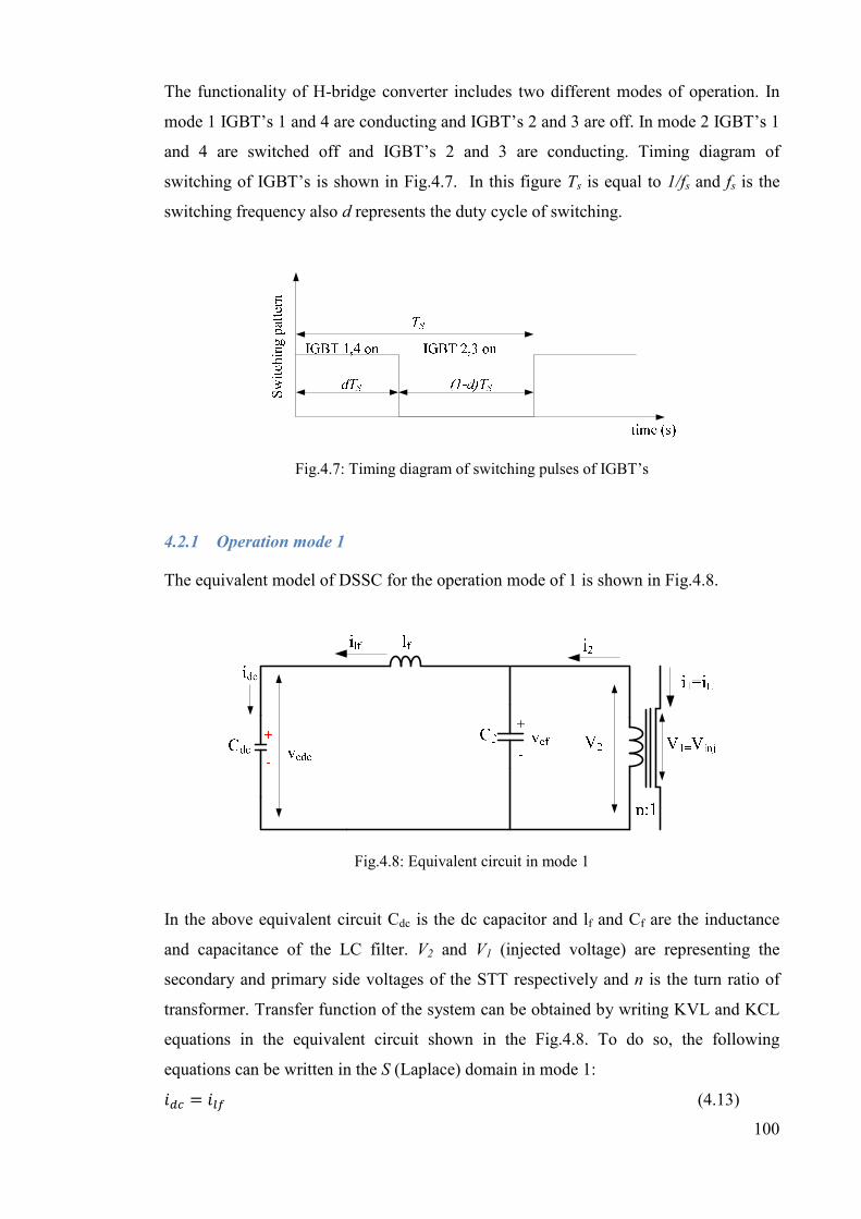
100
The functionality of H-bridge converter includes two different modes of operation. In
mode 1 IGBT’s 1 and 4 are conducting and IGBT’s 2 and 3 are off. In mode 2 IGBT’s 1
and 4 are switched off and IGBT’s 2 and 3 are conducting. Timing diagram of
switching of IGBT’s is shown in Fig.4.7. In this figure Ts is equal to 1/fs and fs is the
switching frequency also d represents the duty cycle of switching.
Fig.4.7: Timing diagram of switching pulses of IGBT’s
4.2.1 Operation mode 1
The equivalent model of DSSC for the operation mode of 1 is shown in Fig.4.8.
Fig.4.8: Equivalent circuit in mode 1
In the above equivalent circuit Cdc is the dc capacitor and lf and Cf are the inductance
and capacitance of the LC filter. V2 and V1 (injected voltage) are representing the
secondary and primary side voltages of the STT respectively and n is the turn ratio of
transformer. Transfer function of the system can be obtained by writing KVL and KCL
equations in the equivalent circuit shown in the Fig.4.8. To do so, the following
equations can be written in the S (Laplace) domain in mode 1: g½r = g·« (4.13)

101
ÀÁ½r(r½r = g½r (4.14)
where ilf and idc are the current passing through the lf and Cdc respectively. In (4.14) vcdc
is the voltage across the Cdc capacitor.
Current through the inductance, ilf, is obtained in the (4.15) by writing KCL equation in
common connection point of STT, lf and Cf .
g·« = g% ·ÂÃÄÅ~?#Æ·ÂÃÂ#%ÃÄ·ÂÇÅ~#(·Â~ÃÂÃÄ#·Â~ÃÄ~ )ÅÈ (4.15)
or
g·« = Xg? [«Á½rÀ%1 + Æ[«Á« + 2Á½r[«ÇÀ% + ([«%Á«Á½r + [«%Á½r% )ÀÉ where i1 and i2 are the primary and secondary current of the SST respectively.
4.2.2 Operation mode 2
In mode 2 the polarity of voltage at the output of the converter will change as shown in
Fig.4.9.
Fig.4.9: Equivalent circuit in mode 2
Voltage across the DC capacitor in mode 2 still can be obtained from (4.14) in the
Laplace domain. However in this mode direction of current passing through the Cdc is
changed and it is presented in (4.16) g½r = −g·« (4.16)
4.2.3 Average of current through DC capacitor
During a period, Ts, we shall assume that DSSC circuit operates in mode 1 and mode 2
for a time period of dTs and Ts(1-d) respectively, where d, as shown in Fig.4.7, is the
duty cycle for switching between mode 1 and mode 2. Considering the fact that the

102
switching frequency, fs, is fast enough to have negligible change in absolute value of the
ilf during mode 1 and mode 2 the average value of idc in one period is obtained in (4.17).
g½r = ½s¬)µÂ#(?½)s¬()µÂ)s¬ = (2i − 1)g·« (4.17)
Voltage across the DC capacitor is recalculated in (4.18) by substituting the average
value of idc in (4.14).
(r½r = (%½?))µÂÅÃÄ (4.18)
By replacing equivalent of ilf from (4.15) in (4.18) vcdc is recalculated in (4.19).
fr½r = Xg? (%½?)·ÂÅ?#Æ·ÂÃÂ#%ÃÄ·ÂÇÅ~#(·Â~ÃÂÃÄ#·Â~ÃÄ~ )ÅÈ (4.19)
in (4.19), (2d-1) is the control term and it can be represented by u. Having considered
this in (4.19) transfer function of vcdc to u is obtained in (4.20).
Ê = Ĩ = Xg? ·ÂÅ?#Æ·ÂÃÂ#%ÃÄ·ÂÇÅ~#(·Â~ÃÂÃÄ#·Â~ÃÄ~ )ÅÈ (4.20)
4.3 Controller design
Employed control strategy is based on the regulating the DC voltage in the desired
value in order to minimize the active power exchange with the AC system. In addition
to the DC voltage regulation the error of multiplication of injected voltage (v1) and line
current (i1) after passing through a low pass filter is being added to the feedback loop in
order to fine tune the injection angle. Block diagram of control strategy is shown in
Fig.4.10.
Fig.4.10: Block diagram of control strategy
In the block diagram shown in Fig.4.10 vcdcRef and vcdc are representing the reference
DC voltage and the voltage across the DC capacitor respectively. Transfer function of
DSSC device is shown by G in the block diagram and it can be obtained, in the Laplace

103
domain, by replacing the values of capacitors and inductance from the system design
parameters (tabulated in Table 4.1) in (4.21).
Component Symbol Value
DC capacitor cdc 500 uF
Filter capacitor cf 500 uF
Filter inductor lf 80 uH
Table 4.1: System parameters
Ê = Ĩ = ?.Ë.zÌÅK.%.zÍÅÈ#?.%.zÌÅ~#? (4.21)
Root Locus diagram of the transfer function, G (transfer function of open loop system),
is presented in Fig.4.11. The right hand side of the diagram (positive real axis) is an
indication of unstable system.
Fig.4.11: Root Locus diagram of the transfer function G
For closed loop system locations of poles and zeroes are shown in Fig.4.12. This figure
shows that, there are two poles in the positive real axis which makes system unstable.
-3 -2.5 -2 -1.5 -1 -0.5 0 0.5 1 1.5
x 104
-3
-2
-1
0
1
2
3x 10
4
0.120.260.40.520.66
0.8
0.9
0.97
5e+03
1e+04
1.5e+04
2e+04
2.5e+04
5e+03
1e+04
1.5e+04
2e+04
2.5e+04
3e+04
0.120.260.40.520.66
0.8
0.9
0.97
Root Locus
Real Axis (seconds-1)
Imaginary Axis (seconds-1)
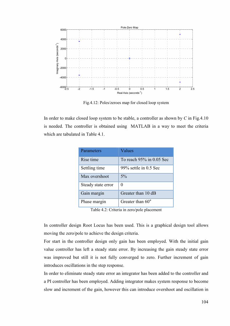
104
Fig.4.12: Poles/zeroes map for closed loop system
In order to make closed loop system to be stable, a controller as shown by C in Fig.4.10
is needed. The controller is obtained using MATLAB in a way to meet the criteria
which are tabulated in Table 4.1.
Parameters Values
Rise time To reach 95% in 0.05 Sec
Settling time 99% settle in 0.5 Sec
Max overshoot 5%
Steady state error 0
Gain margin Greater than 10 dB
Phase margin Greater than 60°
Table 4.2: Criteria in zero/pole placement
In controller design Root Locus has been used. This is a graphical design tool allows
moving the zero/pole to achieve the design criteria.
For start in the controller design only gain has been employed. With the initial gain
value controller has left a steady state error. By increasing the gain steady state error
was improved but still it is not fully converged to zero. Further increment of gain
introduces oscillations in the step response.
In order to eliminate steady state error an integrator has been added to the controller and
a PI controller has been employed. Adding integrator makes system response to become
slow and increment of the gain, however this can introduce overshoot and oscillation in
Pole-Zero Map
Real Axis (seconds-1)
Imaginary Axis (seconds-1)
-2.5 -2 -1.5 -1 -0.5 0 0.5 1 1.5 2 2.5-6000
-4000
-2000
0
2000
4000
6000

105
the step response. It has been noticed that there is a relationship between oscillation in
the step response and poor phase margin. In order to eliminate the oscillations and
improve phase margin, a lead compensator added to the controller. It means that the
controller C shown in Fig. 4.10 includes a PI controller and a lead compensator. The
aforementioned explanation describes the employed approach in the controller design.
In the design process of the controller for start, pole of PI controller is located in “0”
(which is obvious) and MATLAB is used to find the approximate location (first
location) of zero. Root Locus diagram of open loop transfer function after insertion of
zero/pole is plotted in Fig.4.13. Gain of controller has been chosen from the Root Locus
diagram shown in Fig.4.13 in order to respect required criteria of design.
Fig.4.13: Root Locus diagram of the open loop system including controller C
For example, for overshoot of 76.3% and damping factor of 0.0856 the corresponded
gain of 0.0163 can be obtained from Fig.4.13. By including the selected gain in the
controller C the step response of the closed loop system is plotted in Fig.4.14. It can be
observed that peak of overshoot reaches to 1.58 and it oscillates for few cycles before
settling down and reaching steady state.
Root Locus
Real Axis (seconds-1)
Imaginary Axis (seconds-1)
-18 -16 -14 -12 -10 -8 -6 -4 -2 0 2
x 107
-8
-6
-4
-2
0
2
4
6
8x 10
7
0.20.40.580.720.830.91
0.96
0.99
0.20.40.580.720.830.91
0.96
0.99
2e+074e+076e+078e+071e+081.2e+081.4e+081.6e+08

106
Fig.4.14: Step response of closed loop system when gain of controller is 0.0163
The step response of the system can be improved by increasing the damping factor and
reducing the percentage of overshoot. In order to reduce the peak value and suppress the
oscillations overshoot of 0.018% and damping factor of 0.93 has been targeted. The
corresponding gain of 2.85 is obtained from Fig.4.14. In the same time in order to meet
the required gain margin and phase margin of design criteria the lead compensator has
been applied. By moving the zero/pole of the lead compensator using the MATLAB
locations of zero/pole were found in a way to achieve phase margin of 66° and gain
margin of 72 db. Controller C with the designed gain value and zeros/Poles are
represented in (4.22).
Á = 2.85ÏÐp)* ∗ (¡#K.K)¡´ÃÑ*©¢Ñ··.¢ ∗ (¡#Ò.K)(¡#?%.K)-.p½rÑÓÔ.*¡p©Ñ¢ (4.22)
Bode diagram of system with obtained phase margin and gain margin is plotted in
Fig.4.15. The positive values of obtained phase margin and gain margin are showing
system stability.
0 0.2 0.4 0.6 0.8 1 1.2
x 10-6
0
0.2
0.4
0.6
0.8
1
1.2
1.4
1.6Step Response
Time (seconds)
Amplitude

107
Fig.4.15: Bode diagram of system
By applying the newly obtained gain the lead compensator the step response of closed
loop system has been improved as shown in Fig.4.16.
Fig.4.16: Step response of closed loop system meeting overshoot of 0.018% and damping factor of 0.93
In order to validate the designed controller DC voltage across the DC capacitor must be
checked. The designed controller is employed in the simulation of DSSC to control the
operation of system and Fig.4.17 shows the voltage across the DC capacitor. It can be
observed that the voltage is being held in the desired value.
10-15
10-10
10-5
100
105
1010
-225
-180
-135
-90
-45
0
45
90
Frequency (rad/s)
Phase (deg)
-200
-100
0
100
Magnitude (dB)
0 0.1 0.2 0.3 0.4 0.5 0.6 0.7 0.8 0.9 1
x 10-7
0.9
0.92
0.94
0.96
0.98
1
1.02Step Response
Time (seconds)
Amplitude

108
Fig.4.17: Voltage across the DC capacitor
4.4 Sensitivity analysis of designed controller
Effect of change of system parameters on the performance of the designed controller
has been investigated. Change of system parameters includes change in the capacitance
of DC capacitor, AC capacitor (filter capacitor) and inductance of filter. These
parameters can put stability of system at risk by relocating the poles and zeros.
Moreover, the step response of the system and the related overshoot can be affected by
these changes.
4.4.1 Effects of change in the system parameters
System parameters can be changed. For example, capacitance of a capacitor reduces
over time [90] and the reduction can affect the stability and step response of the system.
With the intention of investigating the issue, cdc is reduced by 10%. Resulted step
response and map poles and zeros of closed loop system are presented in Fig.4.18 and
Fig.4.19 respectively. It can be observed that still system is stable and step response is
more or less remains same.
2 2.1 2.2 2.3 2.4 2.5 2.6 2.7 2.8 2.9 30
100
200
300
400
500
600
700
800
900
1000
1100
Time (Seconds)
Voltage [V
]
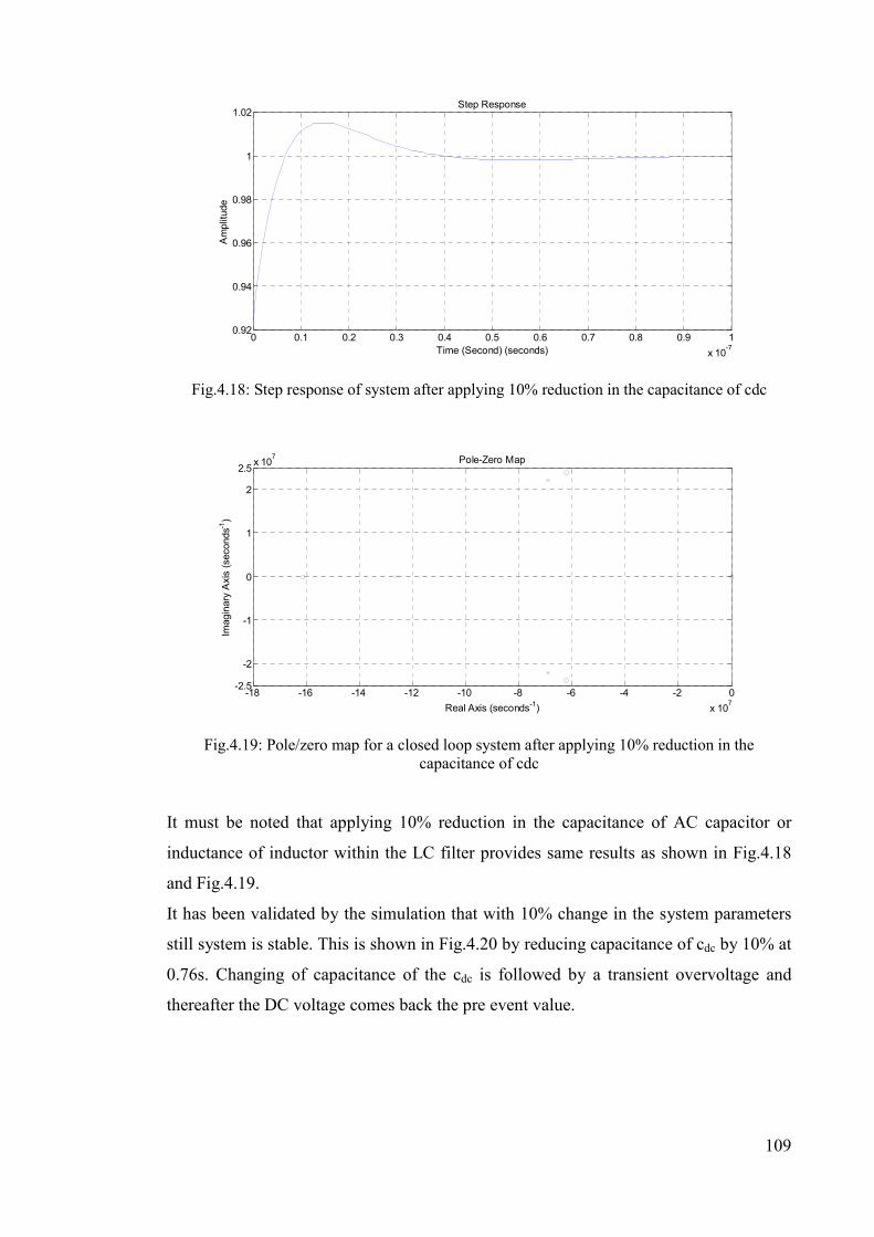
109
Fig.4.18: Step response of system after applying 10% reduction in the capacitance of cdc
Fig.4.19: Pole/zero map for a closed loop system after applying 10% reduction in the capacitance of cdc
It must be noted that applying 10% reduction in the capacitance of AC capacitor or
inductance of inductor within the LC filter provides same results as shown in Fig.4.18
and Fig.4.19.
It has been validated by the simulation that with 10% change in the system parameters
still system is stable. This is shown in Fig.4.20 by reducing capacitance of cdc by 10% at
0.76s. Changing of capacitance of the cdc is followed by a transient overvoltage and
thereafter the DC voltage comes back the pre event value.
0 0.1 0.2 0.3 0.4 0.5 0.6 0.7 0.8 0.9 1
x 10-7
0.92
0.94
0.96
0.98
1
1.02Step Response
Time (Second) (seconds)
Amplitude
-18 -16 -14 -12 -10 -8 -6 -4 -2 0
x 107
-2.5
-2
-1
0
1
2
2.5x 10
7 Pole-Zero Map
Real Axis (seconds-1)
Imaginary Axis (seconds-1)

110
Fig.4.20: Effect of changing capacitance of cdc
However, further reduction in the parameters can lead to instability. For example, with
50% reduction in the cdc, two poles appear in the right hand side of pole/zero map of
closed loop system and it becomes instable. Fig.4.21 and Fig.4.22 show the step
response of system and the pole/zero map after having 50% reduction of capacitance of
cdc.
Fig.4.21: Step response of instable system after applying 50% reduction in capacitance of cdc
Sec 0.40 0.50 0.60 0.70 0.80 0.90 1.00 1.10
-0.2k
0.0
0.2k
0.4k
0.6k
0.8k
1.0k
1.2k
DC Voltage [V]
DC
0 0.1 0.2 0.3 0.4 0.5 0.6 0.7 0.8 0.9 1
x 10-5
-6
-4
-2
0
2
4
6
8
10x 10
24 Step Response
Time (seconds)
Amplitude

111
Fig.4.22: Pole/zero map of closed loop system after applying 50% reduction in capacitance of cdc
Simulation results show that after reducing the capacitance of cdc by 50% system
becomes unstable and DC voltage shown in Fig.4.23 becomes unstable.
Fig.4.23: Instability of system after reducing capacitance of cdc by 50%
4.5 Effect of adding a low pass filter to the proposed controller
Equation (4.7) presents the proposed control strategy for fine tuning and it shows that
the signal includes dc and 2ndorder harmonics. Due to presence of 2nd order harmonics
in this equation (4.2) a low pass filter is needed to be applied in order to eliminate the
harmonics. Transfer function of the employed second order low pas filter is presented in
equation (4.23).
tf6Õ(s) = Ö?#%× Ø²# ز~ (4.23)
-18 -16 -14 -12 -10 -8 -6 -4 -2 0 2
x 107
-4
-3
-2
-1
0
1
2
3
4x 10
7 Pole-Zero Map
Real Axis (seconds-1)
Imaginary Axis (seconds-1)
Sec 0.50 0.60 0.70 0.80 0.90 1.00 1.10
-200.00k
-150.00k
-100.00k
-50.00k
0.00
50.00k
100.00k
150.00k
200.00k
DC Voltage [V]
DC

112
where G is the gain, wc is the cut off frequency of the filter and ξ is the damping factor
of the filter. These parameters for the employed low pass filter within the proposed
controller are provided in Table 4.3.
Parameter Value
G 900
WC 30
ξ 0.7
Table 4.3: Parameters for the employed low pass filter
One of the typical approaches to investigate the performance of a filter is to plot its
frequency response over a range of frequencies. Logarithmic magnitude response of the
low pass filter with presented parameters in Table 4.3 is plotted in Fig.4.24. This figure
shows that DC signals (signals below 1Hz) passes through the filter without any
attenuation however those are above 10Hz have been attenuated based on their
frequency.
In the proposed controller it is required to filter out the AC signals and the frequency
response of the applied filter shows that it well matches with the requirements of the
controller.
Fig.4.24: Logarithmic magnitude response of the low pass filter
However, applying a filter to clean up a signal always raises concern about undesirable
phase delay which in turn can affect the bandwidth of the controller. The phase response
100
101
102
103
-70
-60
-50
-40
-30
-20
-10
0
10
w (rad/s)
LM [dB]
LM Response for Low Pass Filter

113
of the applied low pass filter is plotted in Fig.4.25. It shows higher phase delay for the
high frequency signals and less delay for low frequency signals. In the proposed
controller only DC signal is required to be employed and applied filter must not disturb
it.
Fig.4.25: Phase response of low pass filter
In addition the proposed controller is just for the fine tuning purposes and it is mainly
employed to reduce the error of injection voltage angle in steady state and it is not
expected to contribute toward the transients. In the other hand the phase delay
introduced by low pass filter mainly affects the transient of the system. For this reason 2
or 3 degree phase delay for DC signal created by filter is negligible. This is not affecting
the bandwidth of the main controller (DC voltage controller) as the main controller
operates independently in order to regulate the DC voltage across the DC capacitor.
In the DSSC device because of losses within the converter and other components the
injection angle practically cannot be 90°. However, the target value is 90° and a steady
state error is expected to persist between the reference (target) value and practically
achieved value. It means that steady state error of zero practically is not achievable.
In a PI controller, integrator part corrects the steady state error by accumulating the
error and increasing the amplitude of controller output. The aim is to eliminate the error
in the injected voltage and it means that the angle of injected voltage is desirable to
become exactly 90°. However as discussed earlier this is practically unachievable and
as a result the integrator in the PI controller will keep accumulating the error and
amplitude of the output will increase continuously. Having considered this and taking
into account the steady state error in the injection angle (which controller must live with
100
101
102
103
-180
-160
-140
-120
-100
-80
-60
-40
-20
0
w (rad/s)
φ (w)[deg]
Phase Response for Low Pass Filter
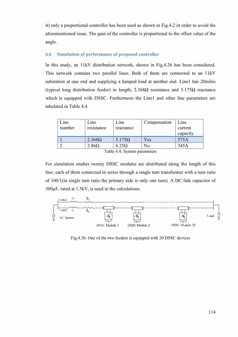
114
it) only a proportional controller has been used as shown in Fig.4.2 in order to avoid the
aforementioned issue. The gain of the controller is proportional to the offset value of the
angle.
4.6 Simulation of performance of proposed controller
In this study, an 11kV distribution network, shown in Fig.4.26 has been considered.
This network contains two parallel lines. Both of them are connected to an 11kV
substation at one end and supplying a lumped load at another end. Line1 has 20miles
(typical long distribution feeder) in length, 2.368Ω resistance and 5.175Ω reactance
which is equipped with DSSC. Furthermore the Line1 and other line parameters are
tabulated in Table 4.4.
Line number
Line resistance
Line reactance
Compensation Line current capacity
1 2.368Ω 5.175Ω Yes 575A
2 2.86Ω 6.25Ω No 345A Table 4.4: System parameters
For simulation studies twenty DSSC modules are distributed along the length of this
line; each of them connected in series through a single turn transformer with a turn ratio
of 100/1(in single turn ratio the primary side is only one turn). A DC link capacitor of
500µF, rated at 1.5kV, is used in the calculations.
Fig.4.26: One of the two feeders is equipped with 20 DSSC devices

115
DSSC device parameters can be found in Table 4.5.
Parameter Value
Capacitance of DC capacitor 500uF
Ratio of STT 1:100
Range of injected voltage Between -10 and 10 volts
Table 4.5: DSSC device parameters
The amount of compensation as a percentage of line reactance can be determined by
adjusting the amplitude of the injected voltage between -10V and 10V depending on the
system’s control strategy. The DSSC devices are seen as a voltage source through the
power line as shown in Fig.4.27.
Fig.4.27: DSSC is seen as a VSC through the power line
The proposed new control strategy, as explained earlier, has been used to control the
DSSC modules through the line1. The PSCAD/EMTDC software is used for simulation
to show that using the proposed controller the DSSC device is able to inject capacitive
and inductive voltage through the line. The simulation results also approve the claimed
advantages of the controller in this chapter.
4.6.1 Capacitive injection
With the intention of investigating the capability of DSSC modules in injecting the
demanded capacitive voltage the devices are set to inject 10 volts in total. The output
voltage of the H-bridge converter which is pulse voltage is shown in the Fig.4.28. The
polarity of the voltage is keep changing based on the switching of the IGBTs in the
converter. Peak value of the output voltage, 1kV, is equal to voltage across the DC
capacitor.

116
Fig.4.28: The output voltage of the converter and its input current
Input current of the converter also is shown in this figure which is proportional to the
line current. The current, passing through the DC link and the current which is fed into
the converter are shown in Fig.4.29. The converter current, as shown in this figure, is
sinusoidal and proportional to the line current. The DC link current clearly shows effect
of switching action. The flow direction of current is being changed in the DC link in
order to charge and discharge the capacitor voltage to hold the DC voltage in a desired
value.
Actually a certain level of DC voltage is required in establishing the output voltage of
the converter. As discussed earlier and shown in Fig.4.28 the output voltage of the
converter is a chain pulse of the DC link voltage with positive and negative polarities.
However the chain pulse is filtered out by LC filter and generates a sinusoidal
waveform with fundamental frequency at the secondary side of the STT. The voltage of
the secondary side of STT along with the associated current is shown in Fig.4.30.
Sec 0.2000 0.2100 0.2200 0.2300 0.2400 0.2500 0.2600 0.2700 0.2800 ...
... ...
-1.0k
-0.5k
0.0
0.5k
1.0k
Voltage [V]
Output Voltage of Converter
-4.0
-3.0
-2.0
-1.0
0.0 1.0
2.0
3.0
4.0
Current [A]
Output Current of Converter

117
Fig.4.29: DC link current and output current of the converter in the capacitive injection mode
Fig.4.30: Voltage and current in the power electronics side of the STT in the capacitive injection mode
The injected voltage through the line is shown in Fig.4.31. It can be seen that the
voltage is leading the line current, and it is a capacitive injection. In order to investigate
the consequences of capacitive voltage injection by DSSC modules, three different
voltages value at 0V, 0.6Vand 1.4Vper each module have been injected. These voltages
are corresponding to 0%, 20% and 50% compensation of phase reactance by DSSC in
the studied power system. Fig.4.32 shows the compensation in three steps. At first there
is no voltage injection, the system is in normal operation and phase current remains
0.0750 0.0800 0.0850 0.0900 0.0950 0.1000 0.1050 0.1100 0.1150 ...
... ...
-4.0
-3.0
-2.0
-1.0
0.0
1.0
2.0
3.0
4.0
Voltage [V]
IDC
-4.0
-3.0
-2.0
-1.0
0.0 1.0
2.0
3.0
4.0
Current [A]
Output Current of Converter
0.420 0.430 0.440 0.450 0.460 0.470 0.480 0.490 ...
... ...
-1.0k
-0.5k
0.0
0.5k
1.0k
Votage [V]
Secondary Voltage
-4.0
-2.0
0.0
2.0
4.0
Current [A
]
Secondary Current

118
unchanged. In the second step the DSSC modules compensate 20 % of the phase
reactance. In order to obtain such compensation it is necessary to inject 12 volts. In the
next step the modules are required to compensate 50% of the reactance, therefore they
inject 28 volts. At the final stage the compensation returned back to 20% and it shows
that the modules can increase or decrease the percentage of compensation.
Fig.4.31: Capacitive injection and voltage is leading the current
Fig.4.32: Capacitive injection in three different levels
Sec 0.700 0.720 0.740 0.760 0.780 ...
... ...
-15.0
-10.0
-5.0
0.0
5.0
10.0
15.0
Injected Voltage [V]
Va-Capacitive Vb-Capacitive Vc-Capacitive
-400 -300
-200 -100
0 100 200
300 400
Line C
urrent [A]
Ia Ib Ic
Sec 0.20 0.40 0.60 0.80 1.00 1.20 1.40 ...
... ...
-40 -30
-20 -10 0
10 20 30
40 50
Injected Voltage [V]
Va-Capacitive Vb-Capacitive Vc-Capacitive
-600
-400
-200
0
200
400
600
Line Current [A]
Ia Ib Ic

119
The consequence of different levels of compensation can be seen in the current of the
compensated line. With injection of capacitive voltage it is expected that the virtual
capacitor to be inserted through the line. This leads to reduction of the reactance of the
line. Less reactance means increment in the line current.
4.6.2 Inductive injection
DSSC modules are able to inject inductive voltage as well because they can effectively
increase the line reactance. This feature is useful in the power flow control when the
operator wants to push away current from a specific line. To do so the final injected
voltage through the line must lag the line current. However the output voltage of the
converter is a pulse voltage and its polarity is changing in different switching condition
and it is shown along with the input current of the converter in Fig.4.33.
Fig.4.33: Output voltage of the converter along with the input current
The DC link current (current passing through the DC capacitor) along with output
current of the converter is shown in Fig.4.34. The flow direction of the current through
the link is being changed frequently to regulate the DC voltage.
Sec 0.2000 0.2100 0.2200 0.2300 0.2400 0.2500 0.2600 0.2700 0.2800 ...
... ...
-1.0k
-0.5k
0.0
0.5k
1.0k
Voltage [V]
Output Voltage of Converter
-4.0
-2.0
0.0
2.0
4.0
Current [A]
Output Current of Converter

120
Fig.4.34: DC link current and output current of the converter in the inductive injection mode
Align with the changing of the flow direction of current in the DC link the polarity of
the output voltage is being changed to synthesize the required voltage at the output of
the converter. The generated voltage (pulse voltage) by the converter is being filtered by
the LC filter. Voltage and current in the secondary side of the STT is shown in Fig.4.35.
This voltage is injected through the line using STT (same as the capacitive injection
mode) and it is shown in Fig.4.36. It shows that the injected voltage is lagging the line
current and the DSSC is capable of injecting of inductive reactance when the proposed
controller is being applied.
In order to examine the inductive injection capability of the DSSC in the test network,
the line reactance is purposely increased by 0%, 20% and 50%. In order to achieve this
compensation levels, lagging voltages of 0V, 12V and 28V have been injected
respectively, as shown in Fig.4.37. In this firstly there is no injection but soon after in
the second time interval the DSSC modules injects 12 V with the purpose of inserting
20 % inductive reactance through the line.
The reduction of the line current shows that the impedance of the line has been
increased as result of the injection. Furthermore in the next time interval the DSSC
modules insert 50 % more inductive reactance and consequently the line current reduces
further. At the final stage again there is no injection and the line current returns back to
the normal, clearly indicating that with voltage injection removed the compensation line
will back to the normal conditions. This shows that the adding capacitive or inductive
0.0750 0.0800 0.0850 0.0900 0.0950 0.1000 0.1050 0.1100 0.1150 ...
... ...
-4.0
-3.0
-2.0
-1.0
0.0
1.0
2.0
3.0
4.0
Voltage [V]
IDC
-4.0
-3.0
-2.0
-1.0
0.0 1.0
2.0
3.0
4.0
Current [A]
Output Current of Converter

121
reactance through the line can be easily achieved. Even the amount of compensation can
be easily altered.
Fig.4.35: Voltage and current in the secondary side of the STT in the inductive injection mode
Fig.4.36: Inductive injection of DSSC modules
0.420 0.430 0.440 0.450 0.460 0.470 0.480 0.490 ...
... ...
-1.0k
-0.5k
0.0
0.5k
1.0k
Votage [V]
Secondary Voltage
-4.0
-2.0
0.0
2.0
4.0
Current [A]
Secondary Current
Sec 0.700 0.720 0.740 0.760 0.780 ...
... ...
-15.0
-10.0
-5.0
0.0
5.0
10.0
15.0
Voltage [V]
Va-Inductive Vb-Inductive Vc-Inductive
-400
-300
-200
-100
0
100
200
300
400
Current [A]
Ia Ib Ic

122
Fig.4.37: Different level of inductive injection
Line1 and line2 are in parallel therefore by increasing the inductance in line1 the current
in this line will decrease and consequently line2 current will increase.
4.7 Comparing performance of proposed controller with 90° phase shift based
controller
Performance of the proposed controller has been compared with 90° phase shift based
controller and dq based controller. The 90 degree phase shift method is used as a control
strategy in the simulation of functionality of DSSC. The phase difference between line
current and injected capacitive voltage is plotted in Fig.4.38. The phase angle using this
controller is -86.85 degree which is different from 90 degree. In this example, the
deviation of 3.15 degree is needed in order to make the system become stable. The
deviation angle shows that there are some losses within the DSSC device and the angle
is diverted from 90 degree to hold DC voltage in the desired value.
Sec 0.20 0.40 0.60 0.80 1.00 1.20 1.40 ...
... ...
-30
-20
-10
0
10
20
30
Injected Voltage [V]
Va-Inductive Vb-Inductive Vc-Inductive
-400
-300
-200
-100
0
100
200
300
400
Line C
urrent [A]
Ia Ib Ic

123
Fig.4.38: Phase difference in capacitive injection mode using the 90° phase shift controller
It must be noted that if the voltage is not injected with a right angle then it will affect
the absorbed active power. If the absorption of active power becomes more than ohmic
losses then the DC voltage will increase. But in the same time voltage regulator will
initiate an error signal to return back the voltage. Consequently the converter needs to
switch between the charge and discharge modes more rapidly in order to maintain the
DC voltage. This dissipates the absorbed power, and additionally, increases amplitude
of the ripples on the DC link voltage.
Losses (or the absorbed active power) inside the DSSC module for 90° phase shift
method is plotted in Fig.4.39 using active power measurement block within the PSCAD.
In this simulation the aim is to compensate 20 % of the line reactance but DSSC device
absorbs active power.
Fig.4.39: Power loss in each DSSC module using the conventional control system
0.00 0.25 0.50 0.75 1.00 1.25 1.50 1.75 2.00 ...
... ...
-90.0
-88.0
-86.0
-84.0
-82.0
-80.0
Degree
PhaseDif
Sec 0.00 0.50 1.00 1.50 2.00 ...
... ...
0
10
20
30
40
50
W
Loss

124
Each DSSC module using the proposed controller consumes 20.33W in order to
compensate the internal power losses while in total all of the modules providing 863.34
VAr to contribute toward the line compensation. However with conventional method
power loss in DSSC module becomes 47.43 watt. System parameters are tabulated in
Table 4.6.
Parameter Value
System voltage 11kV
Line current 575A
Power Line resistance 2.368Ω
Power Line reactance (rated) 5.175Ω
DC link voltage 1.05kV
Number of DSSC device 20
Switching frequency 5kHz
Table 4.6: System parameters
Line current is shown in Fig.4.40. Current, passing through the DC link and the current
is being fed into the converter are shown in Fig. 4.41. The converter current, as shown
in this figure, is sinusoidal and proportional to the line current. The DC link current
clearly, as shown in Fig.4.41, shows effect of switching action. This current is being
chopped frequently to change the flow direction and charge or discharge the capacitor in
order to hold the voltage in a desired value.
Fig.4.40: Line current
Sec 0.090 0.100 0.110 0.120 ...
... ...
-400
-200
0
200
400
Current [A]
I_Line

125
Fig.4.41: Converter current and DC link current
The injection angle is an important factor in regulating the DC voltage across the
capacitor and maintaining the stability of whole system. With the intention of presenting
the difference in the regulated voltages across DC link when using the conventional
approach the DC voltage is shown in Fig.4.42 in more details. Using the 90° phase shift
method the ripple in the DC voltages is 4% which is result of erroneous injection angle.
With the conventional method the peak value is 1130 volts with respect to 1100 volts.
This emphasizes that the method is not more effective in reducing the percentage of
ripples.
Fig.4.42: Ripple of DC voltage (with the conventional method)
Sec 0.090 0.100 0.110 0.120 ...
... ...
-4.5
4.5
Current [A]
I_DClink
-4.5
4.5
Current [A]
I_Hbridge
Sec 1.5050 1.5100 1.5150 1.5200 1.5250 1.5300 1.5350 1.5400 1.5450 1.5500 ...
... ...
1.08k
1.09k
1.10k
1.11k
1.12k
1.13k
1.14k
Voltage [V]
EDC

126
With the conventional method, the harmonic analysis of the injected voltage however
reveals that there are 16% of second order harmonic and 3% of third harmonic along
with the fundamental injected voltage which is shown in Fig.4.43. In this figure the
fundamental voltage is in blue; the green line represents the second harmonics and the
brown one shows the third harmonics.
Fig.4.43: Harmonic analysis of injected voltage using the conventional control method
The proposed controller can optimize the injection phase angle. Supporting for this
feature, the angle of injected voltage with respect to the line current has been
investigated in order to check the accuracy of the controller. The phase difference
between line current and injected capacitive voltage by using the proposed controller is
plotted in Fig.4.44.
Fig.4.44: Phase difference in capacitive injection mode using the proposed controller
0
2
4
6
8
10
12
1 2 3 4 5
Am
pli
tud
e [
V]
Order of Harmonics
0.00 0.25 0.50 0.75 1.00 1.25 1.50 1.75 2.00 ...
... ...
-90.0
-88.0
-86.0
-84.0
-82.0
-80.0
Degree
PhaseDif

127
The phase angle using the proposed controller is -88.65 degree and -86.85 degree with
the conventional control strategy. Comparison between Fig.4.38 and Fig.4.44 shows
that, the angle in using the proposed controller is closer to -90 degree. It must be noted
that if the voltage is not injected with right angle then it will affect the absorbed active
power. If the absorption of active power becomes more than ohmic losses then the DC
voltage will increase. But in the same time voltage regulator will initiate an error signal
to return back the voltage. Consequently the converter needs to switch between the
charge and discharge modes more rapidly in order to regulate the DC voltage. This
dissipates the absorbed power, and additionally, increases amplitude of the ripples on
the DC voltage.
Losses (or the absorbed active power) inside the DSSC module for the proposed control
strategy is plotted in Fig.4.45. In both cases the aim is to compensate 20 % of the line
reactance but different control system absorbs different active power.
Fig.4.45: Power loss in each DSSC module using the proposed control system
The losses within the DSSC modules are measured by using active power measurement
block in the PSCAD software. Each DSSC device using the proposed controller
consumes 20.33W in order to compensate the internal power losses while in total all of
the modules providing 863.34 VAr to contribute toward the line compensation.
However with conventional method power loss in DSSC module becomes 47.43 watt,
which is much higher than that in the proposed method, while they both provide same
reactive power to the system. A summary of above figures including the power losses,
injection phase angle, injected reactive power and percentage of losses in comparison
with the amount of injected reactive power are given in the Table 4.7.
Sec 0.00 0.50 1.00 1.50 2.00 ...
... ...
0.0
5.0
10.0
15.0
20.0
25.0
W
Loss

128
Simulation Results 20% Compensation
Conventional Method Proposed Method
Reactive Power Injection 864.12 VAr 863.34 VAr
Power Loss 47.43 W 20.33 W
Phase angle -86.85 -88.65
Loss percentage 5.4 % 2.3 %
Table 4.7: Summery of power loss and phase angle study
From the table it can be concluded that, in order to inject almost same amount of
reactive power, the proposed method helps to reduce losses from 47.43W to 20.33W per
module, i.e. by 3.1%, when compared to the conventional one.
The injection angle is an important factor in regulating the DC voltage across the
capacitor and maintaining the stability of whole system. With the intention of presenting
the difference in the regulated voltages across DC link when using the new control
method is shown in Fig.4.46 in more details. Using the proposed method the ripple in
the DC voltages is 3.2 % of the peak value, which is 1.05kV. This shows the peak value
is 60 volts less than that in the conventional method. This emphasizes that the proposed
method is more effective in reducing the percentage of ripples compared to the
conventional one.
a) DC voltage across the DC link (with proposed controller)
Sec 0.00 0.25 0.50 0.75 1.00 1.25 1.50 1.75 2.00 ...
... ...
0.0
0.2k
0.4k
0.6k
0.8k
1.0k
1.2k
Voltage [V]
EDC

129
b) Ripple of DC voltage (with proposed controller)
Fig.4.46: Ripple of DC voltage
With harmonic analysis of the injected voltage as shown in Fig.4.47, it is realized that
there is no significant harmonic voltage injection when the proposed method is used.
Fig.4.47: Harmonic voltage injection (using the proposed control method)
Earlier in this chapter it has been claimed that the controller is immune against presence
of harmonics in the power system. This capability has been examined by simulating a
system which is shown in Fig.4.48. In this system V1 is representing the main source
with the fundamental frequency and V2 is demonstrating the harmonic source.
Sec 0.910 0.920 0.930 0.940 0.950 0.960 0.970 0.980 ...
... ...
0.99k
1.00k
1.01k
1.02k
1.03k
1.04k
1.05k
1.06k
1.07k
1.08k
1.09k
Voltage [V]
EDC
0
2
4
6
8
10
12
1 2 3 4 5
Am
pli
tud
e [
V]
Order of Harmonics

130
Fig.4.48: System including harmonics
L1 and L2 are representing the line inductance and the resistance of the line is shown by
R1 and R2. The line current is shown in Fig.4.49 and it includes 5% of fifth harmonic.
The harmonic analysis of the line current is shown in Fig.4.50 and in this figure
amplitude of the fundamental current and fifth harmonic come in blue and pink
respectively.
Fig.4.49: Line current including 5% of fifth harmonics
Sec 0.110 0.120 0.130 0.140 0.150 0.160 0.170 0.180 ...
... ...
-500
-400
-300
-200
-100
0
100
200
300
400
500
Current [A]
LineCurrent

131
Fig.4.50: Harmonic analysis of the line current
The exchanged power between the DSSC device and the AC power system is shown in
Fig.4.51. It can be easily observed from the figure that the AC signal is still symmetrical
and even the DC signal is zero. These show that with presence of harmonics the
controller still works properly, filtering out the polluting harmonics.
Fig.4.51: p(t) ACDC and p(t)DC in presence of 5% 5th harmonic
More extensively, in order to study the probable effect of the harmonics in highly
polluted power systems the functionality of the controller is tested with the presence of
0
50
100
150
200
250
300
350
400
450
1 2 3 4 5
Am
pli
tud
e [
A]
Order of Harmonics
Sec 0.10 0.20 0.30 0.40 0.50 0.60 0.70 0.80 0.90 1.00 ...
... ...
-1.50 -1.00 -0.50 0.00 0.50 1.00 1.50
VA [p.u]
p(t)ACDC
-0.100
-0.050
0.000
0.050
0.100
VA [p.u]
P(t)DC
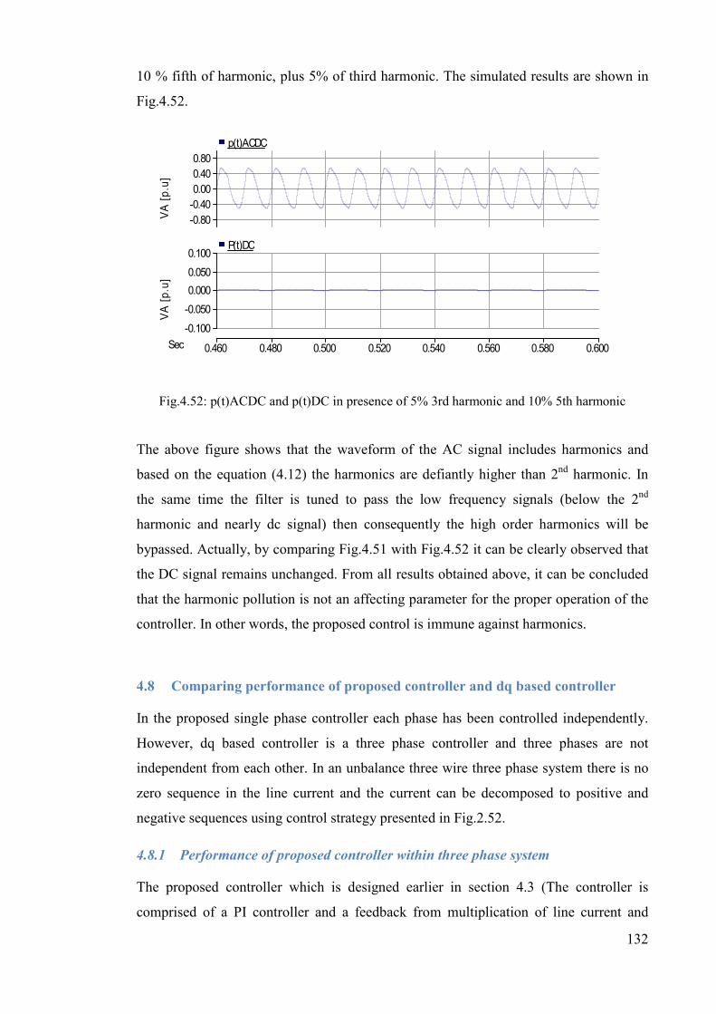
132
10 % fifth of harmonic, plus 5% of third harmonic. The simulated results are shown in
Fig.4.52.
Fig.4.52: p(t)ACDC and p(t)DC in presence of 5% 3rd harmonic and 10% 5th harmonic
The above figure shows that the waveform of the AC signal includes harmonics and
based on the equation (4.12) the harmonics are defiantly higher than 2nd harmonic. In
the same time the filter is tuned to pass the low frequency signals (below the 2nd
harmonic and nearly dc signal) then consequently the high order harmonics will be
bypassed. Actually, by comparing Fig.4.51 with Fig.4.52 it can be clearly observed that
the DC signal remains unchanged. From all results obtained above, it can be concluded
that the harmonic pollution is not an affecting parameter for the proper operation of the
controller. In other words, the proposed control is immune against harmonics.
4.8 Comparing performance of proposed controller and dq based controller
In the proposed single phase controller each phase has been controlled independently.
However, dq based controller is a three phase controller and three phases are not
independent from each other. In an unbalance three wire three phase system there is no
zero sequence in the line current and the current can be decomposed to positive and
negative sequences using control strategy presented in Fig.2.52.
4.8.1 Performance of proposed controller within three phase system
The proposed controller which is designed earlier in section 4.3 (The controller is
comprised of a PI controller and a feedback from multiplication of line current and
Sec 0.460 0.480 0.500 0.520 0.540 0.560 0.580 0.600 ...
... ...
-0.80
-0.40
0.00
0.40
0.80 VA [p.u]
p(t)ACDC
-0.100
-0.050
0.000
0.050
0.100
VA [p.u]
P(t)DC

133
injected voltage which is passing through a low pass filter as described in controller
design section) and presented in equation (4.22) has been applied within a distribution
network. The parameters of the employed distribution power system are tabulated in
Table 4.6 (power system parameters). In this subsection the performance of the
proposed controller in terms of its capability in regulating the DC voltage and injecting
compensation series voltages have been investigated. Control system in each DSSC
module produces its own reference signal without involving with other modules.
Fig.4.53 shows that three DSSC modules employed in three different phases are capable
of regulating the DC voltage within the required value.
Fig.4.53: Voltage across the DC link within DSSC modules employed in three different phases
In order to compare performance of system in supplying balanced load and unbalanced
load these two setups have been investigated. The examined three phase system is
supplying a three phase balanced 6MW load. The line currents and injected voltages by
DSSC devices are shown in Fig.4.54. The figure shows that line currents are balanced
and the injected voltage in each phase is orthogonal to the line current. The reference
signals of injected voltages are shown in Fig.4.55 and they are provided by their own
modules independently. The aim of each controller within DSSC module is to provide
an injected voltage which is orthogonal to the line current and in the same time hold the
DC voltage in desired value. These two requirements have been met by the single phase
controller within three phase system. The simulation results presenting the injected
voltage and their corresponding reference signals have been shown in figure Fig.4.54
and Fig.4.55 respectively.
x 0.350 0.400 0.450 0.500 0.550
0.0
0.2k
0.4k
0.6k
0.8k
1.0k
1.2k
DC Voltage [V]
DCa DCb DCc

134
Fig.4.54: Injected voltages by DSSC devices in each phase and three phase line currents
Fig.4.55: Reference signals of injected voltages provided by each DSSC modules separately
However, the above figures show the performance of the controller when the three
phase system is balanced. In this case the direct and quadrature component of the line
currents (Id and Iq) shown in Fig.4.56 are smooth. This is an indication for a balanced
three phase system. In this figure also the amplitude of the line current is shown by
IdqLine which is equal to:
I79G = I7% + I9% (4.24)
x 0.540 0.550 0.560 0.570 0.580 0.590 0.600 0.610 0.620 0.630
-30
-20
-10
0
10
20
30
Injected Voltage [V]
InjVa InjVb InjVc
-400
-300
-200
-100
0
100
200
300
400
Current [A]
IlineA IlineB IlineC
x 0.190 0.200 0.210 0.220 0.230 0.240 0.250 0.260 0.270
-0.40
-0.30
-0.20
-0.10
0.00
0.10
0.20
0.30
0.40
Referen
ce Signal [p.u]
VAref VBref VCref

135
Fig.4.56: Id, Iq and amplitude of the line current
4.8.2 An unbalanced three phase system with no series compensation
An unbalanced load comprises of a 6MW three phase balanced load and a 1MW single
phase load connected to the phase “b” of three phase distribution system which its
parameters are tabulated in Table 4.6 (the table represents parameters of each phase) has
been simulated. The DSSC devices have been bypassed and the lines are
uncompensated. The injected voltages and line currents are shown in Fig.4.57. It shows
that the injected voltage is zero and line current in phase “b” is higher than the other two
phases. This allows observing the status of distribution system in terms of its dq
components of line current without compensation.
PLL of series compensators are always locked to the line current. However with
unbalance line currents the dq components can be distorted. The Id and Iq components of
line current without compensation along with the amplitude of the line current is plotted
in Fig. 4.58. It can be clearly observed that dq components are oscillatory.
x 0.00 0.10 0.20 0.30 0.40 0.50 0.60 0.70 0.80
0.00
0.10
0.20
0.30
0.40
Current [kA]
Id Iq
0.00
0.10
0.20
0.30
0.40
Current [kA]
IdqLine

136
Fig.4.57: Injected voltage and line currents when the three phase system is unbalanced
Fig.4.58: The Id and Iq components along with the amplitude of the line current
4.8.3 Performance of propsed controller within unbalanced three phase load
In the previous subsection it has been shown that in the presence of unbalanced load the
line currents are unbalanced and dq components are distorted. However simulation
results show that the performance of the single phase controller is not affected by
unbalance of the system. Voltages across the DC link are illustrated in Fig.4.59 and it
shows that the voltage regulation by single phase controller has been satisfactorily
achieved in each phase.
x 0.050 0.100 0.150 0.200 0.250 0.300 0.350 0.400
-0.100
-0.075
-0.050
-0.025
0.000
0.025
0.050
0.075
0.100
Injected Voltage [V]
InjVa InjVb InjVc
-500 -400 -300 -200 -100
0 100 200 300 400 500
Current [A]
IlineA IlineB IlineC
x 0.20 0.30 0.40 0.50 0.60 0.70 0.80 0.90 1.00 1.10
-0.050
0.450
Current [kA]
Id Iq
0.0
0.450
Current [kA]
IdqLine

137
Fig.4.59: DC Voltages
Fig.4.60 shows the reference signals generated by controller within DSSC devices in
different phases. The signals are generated independently and they are not affected by
the unbalanced currents.
Fig.4.60: Reference voltages
The injected voltages by the DSSC devices through the three phase system and the
corresponded line currents are plotted in Fig.4.61. It can be observed that in order to
provide the required compensation the injected voltages only slightly vary depends on
the line current. When the line current is less then injected voltage is high.
The proposed controller is a single phase controller and three phases are completely
independent from each other. In this method each controller in each phase has no
connection to the other phases and it does not sense or control three phase related
components such as zero sequence component.
x 0.500 0.550 0.600 0.650 0.700 0.750 0.800 0.850
-0.2k
0.0
0.2k
0.4k
0.6k
0.8k
1.0k
1.2k
DC Voltage [V]
DCa DCb DCc
x 0.190 0.200 0.210 0.220 0.230 0.240 0.250 0.260 0.270
-0.40
-0.30
-0.20
-0.10
0.00
0.10
0.20
0.30
0.40
Reference Signal [p.u]
VAref VBref VCref

138
Fig.4.61: The injected voltages by DSSC devices and line currents
Injected harmonics by DSSC devices in each phase is demonstrated in Fig.4.62.
Amplitude of injected 3rd harmonics is indicated below each figure. It can be observed
that there are some other high order harmonics as well, however their amplitude is
significantly low in comparison with the fundamental frequency.
x 0.240 0.250 0.260 0.270 0.280 0.290 0.300 0.310 0.320 0.330
-20.0
-15.0
-10.0
-5.0
0.0
5.0
10.0
15.0
20.0
Injected Voltage [V]
InjVa InjVb InjVc
-500 -400 -300 -200 -100
0 100 200 300 400 500
Current [A]
IlineA IlineB IlineC

139
Fig.4.62: Injected harmonics in three phase
4.8.4 Performance of dq based controller within unbalanced three phase load
With the same three phase power system (including the same unbalance load as per
pervious section) conventional dq controller has been employed within the DSSC
devices.
0
0.1
0.2
0.3
0.4
0.5
0.6
0.7
0.8
0.9
1 2 3 4 5 6 7 8 9 10 11 12 13 14 15 16 17 18 19 20 21 22 23 24 25
Am
pli
tud
e [
p.u
]
Order of Harmonics phase A
0
0.1
0.2
0.3
0.4
0.5
0.6
0.7
0.8
0.9
1 2 3 4 5 6 7 8 9 10 11 12 13 14 15 16 17 18 19 20 21 22 23 24 25
Am
pli
tud
e [
p.u
]
Order of Harmonics phase B
0
0.1
0.2
0.3
0.4
0.5
0.6
0.7
0.8
0.9
1
1 2 3 4 5 6 7 8 9 10 11 12 13 14 15 16 17 18 19 20 21 22 23 24 25
Am
pli
tud
e [
p.u
]
Order of Harmonics phase C

140
PI controller dq based controller is designed and the obtained control parameters are
tabulated in Table 4.8. The designed PI controller is used in the unbalanced three phase
system regardless of percentage of system unbalance.
Parameters Value
kp 150
ki 200
Time constant 0.005 Table 4.8: Control parameters
The regulated DC voltages in each phase, shown in Fig.4.63, are slightly different. It
can be observed that the DC voltage in phase “a” is slightly lower than the voltage in
phase “b” and “c”.
Fig.4.63: DC voltages in each phase
The dq components of line currents are shown in Fig.4.64. These components are
oscillatory because the three phase system is unbalanced. Also IdqLine which is calculated
by (4.24) from dq components of three phase line currents is oscillatory. The dq
components of the line current are used in producing reference signals by dq based
controller. The generated reference signals for the three phases are shown in Fig.4.65.
This figure shows that the amplitude of signals are different from each other and they
have unbalanced amplitud.
x 0.450 0.500 0.550 0.600 0.650 0.700 0.750 0.800 0.850 0.900
-0.2k
0.0
0.2k
0.4k
0.6k
0.8k
1.0k
1.2k
DC Voltage [V]
DCa DCb DCc

141
Fig.4.64: dq components and amplitude of the line current
Fig.4.65: Reference signals generated by the dq based controller
The three injected voltages by DSSC devices using dq based controller in three different
phases are shown in Fig.4.66. These voltages are unbalanced and distorted. For example
injected voltage in phase “c” is higher in comparison with the other phases. This is an
unbalance injection and it increases the unbalance of system. In another example
injected voltage in phase “a” is more distorted than the injected voltage in other two
phases.
x 0.00 0.10 0.20 0.30 0.40 0.50 0.60 0.70 0.80 0.90
-0.050
0.450
Current [kA]
Id Iq
0.0
0.450
Current [kA]
IdqLine
x 0.190 0.200 0.210 0.220 0.230 0.240 0.250 0.260 0.270
-0.40
-0.30
-0.20
-0.10
0.00
0.10
0.20
0.30
0.40
Reference Signal [p.u]
VAref VBref VCref

142
Fig.4.66: Injected voltage and line currents
The injected harmonics by the dq based controller in presence of unbalanced load is
shown for each phase in Fig.4.67. The amplitude of injected 3rd harmonics is indicated
below each figure. The presented value is compared with injected 3rd harmonics using a
single phase controller (shown in Fig.4.62). Comparison between Fig.4.62 and Fig.4.67
shows that the amplitude of the harmonics is increased by almost 52%. For example in
the case of phase “a” it is 1.01V in Fig.4.61 and it is 1.94V in Fig.4.67.
The controller uses dq component of three phase system and it does not sense or control
zero sequence component.
When performance of dq based controller is compared with the proposed controller the
followings difference can be identified:
• The reference signals in the proposed controller are not affected by the
unbalance load while they are affected in the dq based controller.
• The injected voltage in the dq based controller is unbalance
• Amplitude of injected harmonics in the dq based controller is high (i.e. 3rd
harmonic almost doubled)
x 0.230 0.240 0.250 0.260 0.270 0.280 0.290 0.300 0.310 0.320 0.330 0.340
-20.0
-15.0
-10.0
-5.0
0.0
5.0
10.0
15.0
20.0
Injected Voltage [V]
InjVa InjVb InjVc
-500 -400 -300 -200 -100
0 100 200 300 400 500
Current [A]
IlineA IlineB IlineC

143
Fig.4.67: Injected harmonics in three phase
0
0.1
0.2
0.3
0.4
0.5
0.6
0.7
0.8
0.9
1
1 2 3 4 5 6 7 8 9 10 11 12 13 14 15 16 17 18 19 20 21 22 23 24 25
Am
pli
tud
e [
p.u
]
Order of Harmonics phase A
0
0.1
0.2
0.3
0.4
0.5
0.6
0.7
0.8
0.9
1
1 2 3 4 5 6 7 8 9 10 11 12 13 14 15 16 17 18 19 20 21 22 23 24 25
Am
pli
tud
e [
p.u
]
Order of Harmonics phase B
0
0.1
0.2
0.3
0.4
0.5
0.6
0.7
0.8
0.9
1
1 2 3 4 5 6 7 8 9 10 11 12 13 14 15 16 17 18 19 20 21 22 23 24 25
Am
pli
tud
e [
p.u
]
Order of Harmonics phase C

144
4.8.5 Performance of proposed controller in presence of unbalance three phase
system
Performance of the proposed single phase controller has been investigated within an
unbalance three phase system. The amplitude of voltages, as shown in Fig.4.68, are
different in each phase and the system is supplying a 6MW balanced load.
Fig.4.68: Amplitude of each phase in the unbalance system
Despite a balance load (in the previous section effect of unbalance load has been
investigated) the supplied current become unbalance and this is shown in dq
representation of load current in Fig.4.69. In this plot it can be observed that there is an
oscillation in the Id and Iq which is an indication for an unbalance system. Amplitude of
IdqLine is calculated by root square of Id plus Iq (dq component of three phase line current)
and it is shown by in Fig.4.69.
Fig. 4.69: dq representation of load current
S 2.160 2.170 2.180 2.190 2.200 2.210 2.220 2.230
-10.0 -7.5 -5.0 -2.5 0.0 2.5 5.0 7.5 10.0
Amplitude [kV]
EaS EbS EcS
S 3.00 3.10 3.20 3.30 3.40 3.50
-0.40 -0.20 0.00 0.20 0.40 0.60 0.80
Current [kA]
Id Iq
0.0
0.450
Current [kA]
IdqLine

145
Calculated reference signals by single phase controllers in each phase are shown in
Fig.4.70. Despite the unbalance system voltage and unbalance load current the
generated signals are identical.
Fig.4.70: Reference signals generated by single phase controller
Injected voltage by DSSC and line current is shown in Fig.4.71. This figure shows that
regardless of unbalance current and voltages in the three phase system, DSSC is able to
inject same voltages in each phase. This shows that the DSSC device in each phase can
execute reference signal without involving with two other phases.
Fig.4.71: Injected voltage by DSSC and line current within unbalance system.
Each DSSC device can hold the demanded DC voltage across its own DC capacitor
independently. This is shown in Fig.4.72 for each phase of system.
S 3.400 3.420 3.440 3.460 3.480 3.500
-0.20
-0.10
0.00
0.10
0.20
Reference Signal [p.u]
VAref VBref VCref
S 4.400 4.420 4.440 4.460 4.480 4.500
-30
-20
-10
0
10
20
30
Injected Voltage [V]
InjVa InjVb InjVc
-500
500
Current [A]
IlineA IlineB IlineC

146
Fig.4.72: Voltages across DC capacitors
Injected harmonics by each DSSC in three phases are shown in Fig.4.73 for phase “a”,
“b” and “c”. The spectrums of harmonics show that the injected harmonics are almost
same.
S 3.400 3.420 3.440 3.460 3.480 3.500
0.0
0.2k
0.4k
0.6k
0.8k
1.0k
DC Voltage [V]
DCa DCb DCc

147
Fig.4.73: Spectrums of injected harmonics by single phase controller in an unbalanced system
0
0.1
0.2
0.3
0.4
0.5
0.6
0.7
0.8
0.9
1
1 2 3 4 5 6 7 8 9 10 11 12 13 14 15 16 17 18 19 20 21 22 23 24 25
Am
pli
tud
e [
p.u
]
Order of Harmonics phase A
0
0.1
0.2
0.3
0.4
0.5
0.6
0.7
0.8
0.9
1
1 2 3 4 5 6 7 8 9 10 11 12 13 14 15 16 17 18 19 20 21 22 23 24 25
Am
pli
tud
e [
p.u
]
Order of Harmonics phase B
0
0.1
0.2
0.3
0.4
0.5
0.6
0.7
0.8
0.9
1
1 2 3 4 5 6 7 8 9 10 11 12 13 14 15 16 17 18 19 20 21 22 23 24 25
Am
pli
tud
e [
p.u
]
Order of Harmonics phase C

148
4.8.6 Performance of dq based controller in presence of unbalance three phase
system
Performance of dq based controller has been examined in presence of an unbalanced
system. This is the same three phase system which has been used in pervious subsection
which performance of the single phase controller has been investigated with. Voltage of
three phase system is shown previously in Fig.4.68 it shows that system has three
different voltages in each phase. Furthermore, dq components of the three phase line
currents because of presence of unbalance are oscillatory as shown in Fig.4.69.
Generated reference signal by the dq based controller is shown in Fig.4.74 and
unbalance of three phase voltage can be observed easily.
Fig.4.74: Generated reference signal by the dq based controller
Fig.4.74 shows that generated reference signal is affected by unbalance of system.
However in pervious subsection by using proposed single phase controller the generated
reference signals, as shown in Fig.4.70 are identical.
Injected voltage by DSSC and line current when dq based controller has been used are
shown in Fig.4.75. This shows that injected voltage is unbalance and its value for each
phase is different.
S 3.400 3.420 3.440 3.460 3.480 3.500
-0.40
-0.30
-0.20
-0.10
0.00
0.10
0.20
0.30
0.40
Reference Signal [p.u]
VAref VBref VCref

149
Fig.4.75: Injected voltage by DSSC using dq based controller
Injected voltage by DSSC using dq based controller is different for each phases while it
is almost identical (as shown in Fig.4.71) when the proposed single phase controller has
been employed.
Using the dq based controller in an unbalanced system is able to regulate the voltage
across the DC capacitor as shown in Fig.4.76.
Fig.4.76: Voltage across the DC capacitor using the dq based controller in an unbalanced system
Comparing Fig.4.72 with Fig.4.76 shows almost no difference between the regulated
voltages across the DC capacitor when single phase controller and dq based controller
has been used respectively.
S 3.400 3.420 3.440 3.460 3.480 3.500
-30
-20
-10
0
10
20
30
Injected Voltage [V]
InjVa InjVb InjVc
-500
500
Current [A]
IlineA IlineB IlineC
S 3.400 3.410 3.420 3.430 3.440 3.450 3.460 3.470 3.480 3.490 3.500
0.0
0.2k
0.4k
0.6k
0.8k
1.0k
DC Voltage [V]
DCa DCb DCc

150
Injected harmonics for three different phases by DSSC when a dq based controller has
been used are shown in Fig.4.77.

151
Fig.4.77: Spectrums of injected harmonics by dq based controller in an unbalanced system
0
0.1
0.2
0.3
0.4
0.5
0.6
0.7
0.8
0.9
1
1 2 3 4 5 6 7 8 9 10 11 12 13 14 15 16 17 18 19 20 21 22 23 24 25
Am
pli
tud
e [
p.u
]
Order of Harmonics phase A
0
0.1
0.2
0.3
0.4
0.5
0.6
0.7
0.8
0.9
1
1 2 3 4 5 6 7 8 9 10 11 12 13 14 15 16 17 18 19 20 21 22 23 24 25
Am
pli
tud
e [
p.u
]
Order of Harmonics phase B
0
0.1
0.2
0.3
0.4
0.5
0.6
0.7
0.8
0.9
1
1 2 3 4 5 6 7 8 9 10 11 12 13 14 15 16 17 18 19 20 21 22 23 24 25
Am
pli
tud
e [
p.u
]
Order of Harmonics phase C

152
Comparing spectrums of injected harmonics by two controllers shows that amplitude of
third harmonics using dq based controller is boosted almost ten times in phase B and
four times in phase C.
4.9 Comparing the performance of proposed controller with using only a DC
link voltage controller
Performance of DSSC using only DC voltage controller and proposed controller has
been compared. In Fig.4.78 concept of both controllers have been presented and it has
been shown that only one controller can be selected in a time by using contrller selector.
This figure provides blockdiagramatic comparsion between the two controllers. As it
can be clearly observed that conventional controller (only DC voltage controller)
recieves only error of DC voltage as an input and consequently it controls only this
parameter. However in proposed controller (located inside the green dasht line) in order
to provide reference signal not only the error of DC voltage is being taken into account
but also the error of injection angle has been considered. It means that proposed
controller, controls both injection angle and DC voltage. The proposed controller in
absense of phase difference signal is the same as the convetional controller. The
conventional controller alone can adjust the DC voltage however the injection angle can
be sacrifised. This is because it controls only the DC voltage and tries to keep the DC
voltage as close as possible to refrence value. In this approach injection angle is not in
priorety and it is used by DC voltage controller to provide required active power to hold
the DC voltage.
However the injection angle itself in DSSC device is required to be kept fixed and as
close as possible to 90° and it needs to be considered by the controller. By adding the
phase difference (which is shown in green in Fig.4.78) in the proposed controller both
DC voltage and injection angle will be considered.

153
Fig.4.78: Comparison between the proposed controller and DC voltage (only) controller
4.9.1 Performance of the device using voltage regulator only
DC regulator alone can be used to hold the DC voltage in DSSC device and inject series
voltage through the line. DC voltage controller is an optimaly tuned PI contoller using
root locus approach.
In the DC voltage controller as shown in Fig.4.1 controller regulates the voltage across
the DC capacitor. Transfer function of DSSC device is shown by G in the block
diagram and it is represented in (4.25)
Ê = Ĩ = ?.Ë.zÌÅK.%.zÍÅÈ#?.%.zÌÅ~#? (4.25)
Root Locus diagram of G is shown in Fig.4.79. There are two branches that move to the
positive side and the system is unstable.

154
Fig.4.79: Root Locus diagram of G
A controller is needed to be designed to stabilize the system and meet the requirements
which are tabulated in Table 4.9. The requirements in this table are chosen in a way to
be consistent with other designed controllers in this chapter.
Parameter Value
Overshoot Less than 5%
Damping 0.9
Table 4.9: Requirements for the designed controller
By inserting a zero and pole the Locus is changed as shown in Fig. 4.80. The change of
Locus is not guaranteeing that the controller is meeting the requirements. The step
response of the system needs to be seen in order to evaluate the system performance.
The step response is plotted in Fig. 4.81 and it shows high oscillation in response.
Fig. 4.80: Root Locus with inserted zero and pole
-3 -2.5 -2 -1.5 -1 -0.5 0 0.5 1 1.5
x 104
-3
-2
-1
0
1
2
3x 10
4
0.120.260.40.520.66
0.8
0.9
0.97
5e+03
1e+04
1.5e+04
2e+04
2.5e+04
5e+03
1e+04
1.5e+04
2e+04
2.5e+04
3e+04
0.120.260.40.520.66
0.8
0.9
0.97
Root Locus
Real Axis (seconds-1)
Imaginary Axis (seconds-1)
-8 -7 -6 -5 -4 -3 -2 -1 0 1 2
x 108
-4
-3
-2
-1
0
1
2
3
4x 10
8
0.20.40.580.720.830.91
0.96
0.99
0.20.40.580.720.830.91
0.96
0.99
1e+082e+083e+084e+085e+086e+087e+088e+08
Real Axis
Imag Axis

155
Fig. 4.81: Step response with inserted zero and pole
In order to eliminate the oscillation the inserted zero needs to be relocated in a way to
improve the step response. To do so, inserted zero is moved further right to -1.34 and
the corresponding Root Locus diagram is plotted in Fig. 4.82.
For overshoot of less than 5% and damping factor of 0.95 the corresponded gain of 150
can be obtained from Root Locus in Fig. 4.82. By including the selected gain in the
controller the corresponding step response of the system is plotted in Fig. 4.83. It can be
observed that peak of overshoot reaches to 1.04 and there is no oscillation before
settling down and reaching steady state.
Fig. 4.82: Root Locus when inserted zero is moved further to the right
Time (seconds)
Amplitude
0 0.5 1 1.5 2 2.5
x 10-6
0
0.2
0.4
0.6
0.8
1
1.2
1.4
1.6
1.8
2
-10 -8 -6 -4 -2 0 2
x 108
-6
-4
-2
0
2
4
6
x 107
0.860.9650.9860.9940.9970.998
0.999
1
1
0.860.9650.9860.9940.997
0.998
0.999
1
12e+084e+086e+088e+081e+09
Real Axis
Imag Axis

156
Fig. 4.83: Step response of the system when inserted zero is moved further to the right
Parameters of the PI controller are calculated in (4.26) by comparing the inserted pole
and zero with the transfer function of controller. The inserted zero and pole are -1.34
and 0 respectively and the gain is 150 (from Root Locus).
?ÙI(¡#?.KÉ)¡ = (ÚÛ¡#ÚÜ)¡ (4.26)
From (4.26) kp and ki are obtained 150 and 200 and tabulated in Table 4.10.
Parameters Value
kp 150
ki 200
Table 4.10: Parameters of PI controller
The injected angle (phase difference between injected voltage and line current) in each
phase by DSSC devices is presented in Fig. 4.84. The angle is varying in order to
regulate the DC voltage and for phase “A” the variation is around 95.85°. It means that
it is deviated from 90° by 5.85°.
Step Response
Time (seconds)
Amplitude
0 0.2 0.4 0.6 0.8 1 1.2 1.4 1.6 1.8 2
x 10-8
0
0.2
0.4
0.6
0.8
1
1.2

157
Fig. 4.84: Phase difference between injected voltage and line current in each phase
Obviously, the aim of this controller is just to adjust the voltage across the DC link and
it has no direct control on the angle of injected voltage.
The DC voltage using voltage regulator only, is plotted in Fig.4.85 for three different
phases. In steady state the voltage in DC link of each DSSC devices varies between
977V and 1020V and amplitude of rippel is 43V.
Fig.4.85: DC voltages in three different phases
Sec 1.00 1.20 1.40 1.60 1.80 2.00
95.60
95.70
95.80
95.90
96.00
96.10
Angle [Degree]
PhsDifA
95.60
95.70
95.80
95.90
96.00
96.10
Angle [Degree]
PhsDifB
95.60
95.70
95.80
95.90
96.00
96.10
Angle [Degree]
PhsDifC
x 1.5925 1.5950 1.5975 1.6000 1.6025 1.6050 1.6075 1.6100 1.6125 1.6150 1.6175
0.970k
0.975k
0.980k
0.985k
0.990k
0.995k
1.000k
1.005k
1.010k
1.015k
1.020k
1.025k
1.030k
DC Voltage [V]
DCa DCb DCc

158
The injected harmonics by DSSC device are plotted in Fig.4.86. The harmonic spectrum
shows that, along with the fundamental frequency the device injects some other
harmonics such as 3rd and 20th. Total harmonic distortion (THD) of injected voltage is
5%.
Amplitude of the 3rd harmonics is indicated below each harmonic spectrum for each
phase. For example in phase “A” amplitude of 3rd harmonic is 0.98V.

159
Fig.4.86: Injected harmonics by DSSC device
0
0.1
0.2
0.3
0.4
0.5
0.6
0.7
0.8
0.9
1 3 5 7 9 11 13 15 17 19 21 23 25 27 29
Am
pli
tud
e [
p.u
]
Order of Harmonics
0
0.1
0.2
0.3
0.4
0.5
0.6
0.7
0.8
0.9
1 3 5 7 9 11 13 15 17 19 21 23 25 27 29
Am
pli
tud
e [
p.u
]
Order of Harmonics phase B
0
0.1
0.2
0.3
0.4
0.5
0.6
0.7
0.8
0.9
1 3 5 7 9 11 13 15 17 19 21 23 25 27 29
Am
pli
tud
e [
p.u
]
Order of Harmonics phase C

160
The PI controller gain is changed at different values around the optimally obtained
value (150 as per Table 4.10) in order to investigate the effect of different gains on the
performance of system. The changes in the gain values affect the ripples of DC voltages
and the injected angle. Depends on if the gain is increased or decreased the obtained
results can be different. Fig. 4.87-Fig.4.94 show the obtained results for ±10% change
of the gain.
In Fig. 4.87 the voltage across the DC link has been increased as the gain of PI
controller is increased by 10%. The peak voltage increased from 1.02 kV to 1.03 kV
and the ripple is 75V. The increment of ripples amplitude as a result of increasing the
gain is not a desirable effect.
The injection angle is presented in Fig. 4.88 and it shows that the angle is improved as
result of higher gain when it is compared with Fig. 4.84. The angle is reduced from
95.9° to 95.7° and it is a desirable effect.
The injected harmonics by DSSC device is represented in Fig. 4.89. By comparing the
amplitude of harmonics with the harmonics plotted in Fig.4.86 it can be observed that
amplitude of injected harmonics is slightly increased and THD is obtained 5.2%.
Fig. 4.87: Voltages across the DC capacitor when the PI gain is increased
Time [s] 1.9250 1.9300 1.9350 1.9400 1.9450 1.9500
0.950k
0.960k
0.970k
0.980k
0.990k
1.000k
1.010k
1.020k
1.030k
1.040k
DC Voltage [V]
DCa DCb DCc

161
Fig. 4.88: Injection angle when gain in the PI controller is increased
Sec 0.40 0.60 0.80 1.00 1.20 1.40
95.60
95.70
95.80
95.90
96.00
96.10
Angle [Degree]
PhsDifA
95.60
95.70
95.80
95.90
96.00
96.10
Angle [Degree]
PhsDifB
95.60
95.70
95.80
95.90
96.00
96.10
Angle [Degree]
PhsDifC
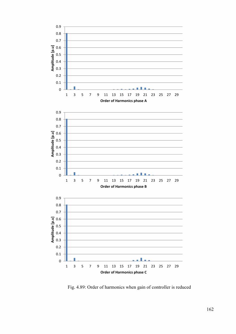
162
Fig. 4.89: Order of harmonics when gain of controller is reduced
0
0.1
0.2
0.3
0.4
0.5
0.6
0.7
0.8
0.9
1 3 5 7 9 11 13 15 17 19 21 23 25 27 29
Am
pli
tud
e [
p.u
]
Order of Harmonics phase A
0
0.1
0.2
0.3
0.4
0.5
0.6
0.7
0.8
0.9
1 3 5 7 9 11 13 15 17 19 21 23 25 27 29
Am
pli
tud
e [
p.u
]
Order of Harmonics phase B
0
0.1
0.2
0.3
0.4
0.5
0.6
0.7
0.8
0.9
1 3 5 7 9 11 13 15 17 19 21 23 25 27 29
Am
pli
tud
e [
p.u
]
Order of Harmonics phase C
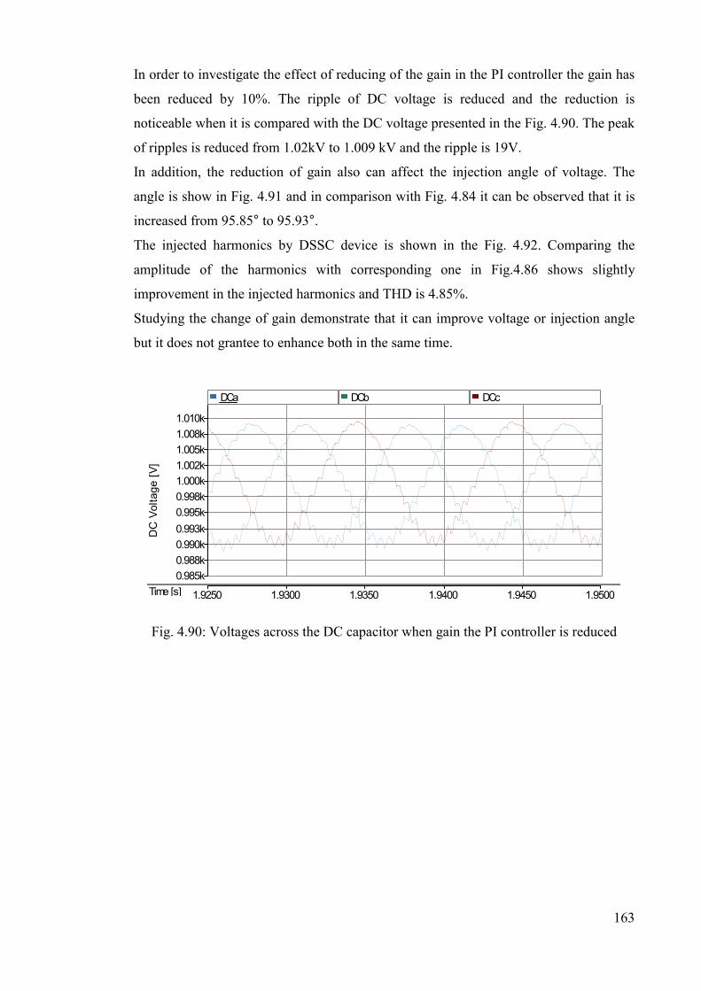
163
In order to investigate the effect of reducing of the gain in the PI controller the gain has
been reduced by 10%. The ripple of DC voltage is reduced and the reduction is
noticeable when it is compared with the DC voltage presented in the Fig. 4.90. The peak
of ripples is reduced from 1.02kV to 1.009 kV and the ripple is 19V.
In addition, the reduction of gain also can affect the injection angle of voltage. The
angle is show in Fig. 4.91 and in comparison with Fig. 4.84 it can be observed that it is
increased from 95.85° to 95.93°.
The injected harmonics by DSSC device is shown in the Fig. 4.92. Comparing the
amplitude of the harmonics with corresponding one in Fig.4.86 shows slightly
improvement in the injected harmonics and THD is 4.85%.
Studying the change of gain demonstrate that it can improve voltage or injection angle
but it does not grantee to enhance both in the same time.
Fig. 4.90: Voltages across the DC capacitor when gain the PI controller is reduced
Time [s] 1.9250 1.9300 1.9350 1.9400 1.9450 1.9500
0.985k
0.988k
0.990k
0.993k
0.995k
0.998k
1.000k
1.002k
1.005k
1.008k
1.010k
DC Voltage [V]
DCa DCb DCc

164
Fig. 4.91: Injection angle when gain the PI controller is reduced
Sec 0.80 1.00 1.20 1.40 1.60 1.80 2.00 2.20
95.60
95.70
95.80
95.90
96.00
96.10
Angle [Degree]
PhsDifA
95.60
95.70
95.80
95.90
96.00
96.10
Angle [Degree]
PhsDifB
95.60
95.70
95.80
95.90
96.00
96.10
Angle [Degree]
PhsDifC

165
Fig. 4.92: Order of harmonics when gain of controller is increased
0
0.1
0.2
0.3
0.4
0.5
0.6
0.7
0.8
0.9
1
1 3 5 7 9 11 13 15 17 19 21 23 25 27 29
Am
pli
tud
e [
p.u
]
Order of Harmonics phase A
0
0.1
0.2
0.3
0.4
0.5
0.6
0.7
0.8
0.9
1
1 3 5 7 9 11 13 15 17 19 21 23 25 27 29
Am
pli
tud
e [
p.u
]
Order of Harmonics phase B
0
0.1
0.2
0.3
0.4
0.5
0.6
0.7
0.8
0.9
1
1 3 5 7 9 11 13 15 17 19 21 23 25 27 29
Am
pli
tud
e [
p.u
]
Order of Harmonics phase C

166
4.9.2 Performance of the device using proposed controller
DC voltage controller can be re-tuned (fine tuning) to improve ripples or reduce
deviation of injection angle. This requires fine tuning parameters of PI controller
however proposed controller considers both DC voltage adjustment and angle of
injection in the same time. It is expected that the ripple of voltages to be lower and
angle of injection to be closer to the 90° by employing the proposed controller. By
further tuning the proposed controller it can be observed that the angle of injection is
reduced to 95.05°. The angle of injection in each phase is plotted in Fig.4.93.
Fig.4.93: Injection angle
In the same time DC voltage ripple become 15V and the voltage oscillates between
987V and 1002V. The boundary of oscillation is reduced by 65 % in comparison with
DC voltage shown in Fig.4.85. The boundary of oscillation is 43V (using only DC
voltage controller) in Fig.4.85 while it is 15V in Fig.4.94. The DC voltage adjusted by
each DSSC devices in three different phases is plotted in Fig.4.94.
The importance of the proposed controller becomes dominant when accuracy of
injection angle come high priority.
Sec 1.00 1.20 1.40 1.60 1.80 2.00
94.80
94.90
95.00
95.10
95.20
95.30
Angle [Degree]
PhsDifA
94.80
94.90
95.00
95.10
95.20
95.30
Angle [Degree]
PhsDifB
94.80
94.90
95.00
95.10
95.20
95.30
Angle [Degree]
PhsDifC

167
Fig.4.94: DC voltage using the proposed controller
The spectrum of injected harmonics using the proposed controller is presented in
Fig.4.95 for three different phases. Amplitude of injected 3rd harmonic through phase
“A” is 0.71V which in comparison with its value represented in pervious figure is
reduced by 27%. THD of injected voltage is 4.1%.
Sec 1.0000 1.0050 1.0100 1.0150 1.0200 1.0250
0.984k
0.987k
0.990k
0.993k
0.996k
0.999k
1.002k
1.005k
DC Voltage [V]
DCa DCb DCc

168
Fig.4.95: Injected harmonics using the proposed controller
0
0.1
0.2
0.3
0.4
0.5
0.6
0.7
0.8
0.9
1
1 2 3 4 5 6 7 8 9 10 11 12 13 14 15 16 17 18 19 20
Am
pli
tud
e [
p.u
]
Order of Harmonics phase A
0
0.1
0.2
0.3
0.4
0.5
0.6
0.7
0.8
0.9
1
1 2 3 4 5 6 7 8 9 10 11 12 13 14 15 16 17 18 19 20
Am
pli
tud
e [
p.u
]
Order of Harmonics phase B
0
0.1
0.2
0.3
0.4
0.5
0.6
0.7
0.8
0.9
1
1 2 3 4 5 6 7 8 9 10 11 12 13 14 15 16 17 18 19 20
Am
pli
tud
e [
p.u
]
Order of Harmonics phase C

169
4.9.3 Summarized results of conventional and proposed controller
In the conventional controller when gain increases, it affects the voltage ripples, THD
and the angle of injection. Amplitude of ripples and angle of injection respond
differently to the change of gain. Increment of gain improves the angle while increases
the amplitude of ripples and THD. It means that improving one the factors (i.e injection
angle) sacrifices the other one.
However, when gain is reduced it reduces the amplitude of ripples and THD, but
increases the injection angle. It can be observed that reducing gain does not improve all
factors in the same time.
Proposed controller can improve ripples, THD and injection angle in the same time as it
receives continuously feedback from both angle of injection and DC voltage. These
improvements (as shown in the previous subsection) have been achieved by further
tuning the proposed controller. The ripple is reduced to 15V and angle of injection is
reduced to 95.05°.
Table 4.11 summarizes the simulation results for the further tuned conventional and
proposed controller.
Controller kp ki Ripple Angle THD
Conventional controller 150 200 43V 95.9° 5%
Conventional controller with increase gain 165 200 75V 95.7° 5.2%
Conventional controller with reduced gain 135 200 19V 95.93° 4.85%
Proposed controller with further tuning 142 200 15V 95.05° 4.1%
Table 4.11: Summarized results of further tuned conventional and proposed controller
4.10 Investigation of the change of the system parameters on the performance of
the proposed controller
In electrical networks (including distribution feeders) some of the system parameters
such as line voltage, connected load and network configuration can be changed with
different loading conditions. For example, voltage drop can often happen in heavily
loaded distribution networks and in another example, amplitude of line current can be
altered by changing loads in the system. However, it is expected that the functionality of

170
DSSC which is governing by the proposed controller not to be affected by these
changes.
4.10.1 Performance of the DSSS with no changes in system parameters
An 11Kv distribution feeder supplying a three phase load is equipped with DSSC
devices have been used in simulation. Impedance of the line comprises of 0.03 H
reactance and 1 Ω resistance. DC voltage as shown in Fig. 4.96 has been regulated at
1kV by each DSSC devices in their own DC link.
Fig. 4.96: DC voltage when line impedance includes 0.03 H reactance and 1Ω resistance
Injected voltage and line current is shown in Fig.4.97 and it shows the orthogonal
injection of voltage through the line and peak amplitude of line current flowing through
the STT is 380A.
x 0.000 0.050 0.100 0.150 0.200 0.250 0.300 0.350 0.400
-0.2k
0.0
0.2k
0.4k
0.6k
0.8k
1.0k
1.2k
DC Voltage [V]
DCa DCb DCc

171
Fig.4.97: Line Current and injected voltage when line impedance includes 0.03H reactance and 1Ω resistance
Load angle between the sending end and receiving end is show in Fig.4.98. The angle
is 23.8° when the line peak current is 380A. It can change depends on the impedance of
the line and this is shown in the next subsection.
Fig.4.98: Load angle when line impedance includes 0.03 H reactance and 1Ω resistance
4.10.2 Performance of the DSSS when resistance of the line is altered
Line resistance reduced by 90% from 1Ω to 0.1Ω in order to investigate the effect of
change of the line resistance on the performance of the DSSC. As a result of reduction
x 3.520 3.530 3.540 3.550 3.560 3.570 3.580 3.590
-20
-10
0
10
20
Injected Voltage [V]
InjVa InjVb InjVc
-400 -300
-200 -100
0 100 200
300 400
Current [A]
IlineA IlineB IlineC
x 0.50 1.00 1.50 2.00 2.50 3.00
20.0
21.0
22.0
23.0
24.0
25.0
Angle [Degree]
SnRvEndPhsDif

172
of the line resistance, current is increased from 380A to 400A. This increment can be
realized by comparing Fig.4.99 and Fig.4.97.
Fig.4.99: Line Current and injected voltage when resistance of the line is 0.1Ω
Fig.4.99 shows that injected voltage is orthogonal to the line current and it has not been
affected by change of line current.
The load angle is shown in Fig.4.100 and due to the reduction in the resistivity of the
line, load angle is increased by 1° from 23.8° to 24.8°.
Fig.4.100: Load angle when resistance of the line is 0.1Ω
x 0.630 0.640 0.650 0.660 0.670 0.680 0.690 0.700 0.710
-20.0
-15.0
-10.0
-5.0
0.0
5.0
10.0
15.0
20.0 Injected Voltage [V]
InjVa InjVb InjVc
-400 -300
-200 -100
0 100 200
300 400
Current [A]
IlineA IlineB IlineC
x 0.40 0.50 0.60 0.70 0.80
22.0
23.0
24.0
25.0
26.0
Angle [Degree]
SnRvEndPhsDif

173
Despite the changes in the line current, line impedance and load angle the proposed
controller has regulated the voltage across the DC link at 1kv (desired value). DC
voltages are plotted in Fig.4.101 and it shows that performance of the controller has not
been affected by the aforementioned changes.
Fig.4.101: DC voltage when resistance of the line is 0.1Ω
4.10.3 Performance of the DSSS when load is reduced in half
Variation of the load occurs most frequently in the electrical networks especially in the
distribution networks. DSSC models employed in the networks need to be compatible
with such changes. It means that employed controller must operate in presence of
different loads and be able to regulate the DC voltage in a required value and inject
orthogonal voltage with respect to the line current. Fig.4.102 shows the voltage across
the DC link when the supplied load is halved. It can be seen that the voltage is regulated
in 1kV and it remains stable in steady state regardless of load reduction.
x 0.000 0.050 0.100 0.150 0.200 0.250 0.300 0.350 0.400 0.450
-0.2k
0.0
0.2k
0.4k
0.6k
0.8k
1.0k
1.2k
DC Voltage [V]
DCa DCb DCc

174
Fig.4.102: Voltage across the DC link when the supplied load is halved
With load shading line current as shown in Fig.4.103 has been reduced almost by 50%
from 400A to 200A. However as it can be observed the DSSC modules are still able to
inject orthogonal voltage through the line. This shows that operation of controller is not
dependent on the line current and it can operate satisfactorily with different line
currents.
Fig.4.103: Line current and injected voltage when the supplied load is halved
However, the load angle has been changed by change of the connected load at the
receiving end and it is shown in Fig.4.104. Comparison between this figure with the
corresponding one shows that load angle has been decreased by 45% from 23.8° to
x 0.00 0.10 0.20 0.30 0.40 0.50 0.60 0.70
-0.2k
0.0
0.2k
0.4k
0.6k
0.8k
1.0k
1.2k
DC Voltage [V]
DCa DCb DCc
x 0.480 0.490 0.500 0.510 0.520 0.530 0.540 0.550 0.560 0.570
-30
-20
-10
0
10
20
30
Injected Voltage [V]
InjVa InjVb InjVc
-250 -200 -150 -100 -50 0 50 100 150 200 250
Current [A]
IlineA IlineB IlineC
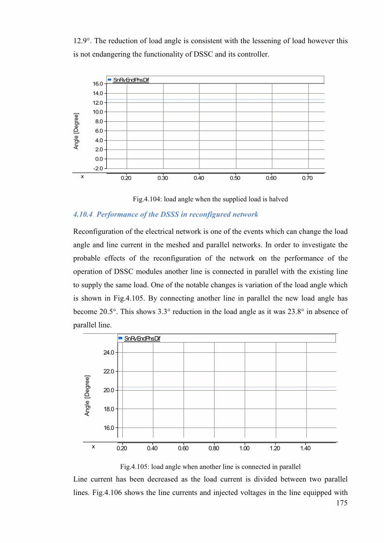
175
12.9°. The reduction of load angle is consistent with the lessening of load however this
is not endangering the functionality of DSSC and its controller.
Fig.4.104: load angle when the supplied load is halved
4.10.4 Performance of the DSSS in reconfigured network
Reconfiguration of the electrical network is one of the events which can change the load
angle and line current in the meshed and parallel networks. In order to investigate the
probable effects of the reconfiguration of the network on the performance of the
operation of DSSC modules another line is connected in parallel with the existing line
to supply the same load. One of the notable changes is variation of the load angle which
is shown in Fig.4.105. By connecting another line in parallel the new load angle has
become 20.5°. This shows 3.3° reduction in the load angle as it was 23.8° in absence of
parallel line.
Fig.4.105: load angle when another line is connected in parallel
Line current has been decreased as the load current is divided between two parallel
lines. Fig.4.106 shows the line currents and injected voltages in the line equipped with
x 0.20 0.30 0.40 0.50 0.60 0.70
-2.0
0.0
2.0
4.0
6.0
8.0
10.0
12.0
14.0
16.0
Angle [Degree]
SnRvEndPhsDif
x 0.20 0.40 0.60 0.80 1.00 1.20 1.40
16.0
18.0
20.0
22.0
24.0
Angle [Degree]
SnRvEndPhsDif

176
DSSC modules. Line current was 400A when a single line was supplying the load (see
Fig.4.88) however by connecting another line in parallel, line current becomes 260A.
Although line current and load angle (as it is discussed earlier) has been changed but
satisfactory orthogonal voltage injection plotted in Fig.4.106 shows the performance of
the controller has not been affected.
Fig.4.106: Line Current and injected voltage when another line is connected in parallel
Voltage across the DC link is shown in Fig.4.107 and it shows that despite change of
load angle and line current controller is able to regulate the DC voltage at 1kV. Voltage
remain stable in steady state and its amplitude is not affected by the changes in the
power system.
x 0.470 0.480 0.490 0.500 0.510 0.520 0.530 0.540 0.550 0.560 0.570 0.580
-30
-20
-10
0
10
20
30
Injected Voltage [V]
InjVa InjVb InjVc
-300
-200
-100
0
100
200
300
Current [A]
IlineA IlineB IlineC
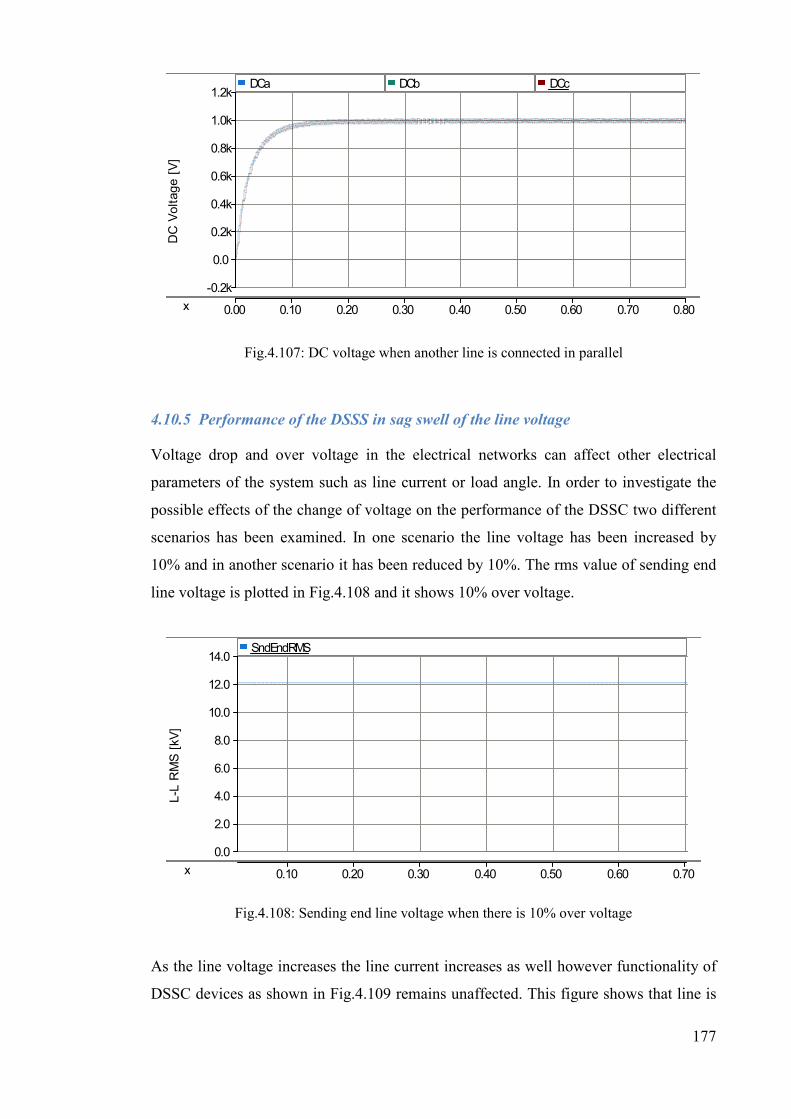
177
Fig.4.107: DC voltage when another line is connected in parallel
4.10.5 Performance of the DSSS in sag swell of the line voltage
Voltage drop and over voltage in the electrical networks can affect other electrical
parameters of the system such as line current or load angle. In order to investigate the
possible effects of the change of voltage on the performance of the DSSC two different
scenarios has been examined. In one scenario the line voltage has been increased by
10% and in another scenario it has been reduced by 10%. The rms value of sending end
line voltage is plotted in Fig.4.108 and it shows 10% over voltage.
Fig.4.108: Sending end line voltage when there is 10% over voltage
As the line voltage increases the line current increases as well however functionality of
DSSC devices as shown in Fig.4.109 remains unaffected. This figure shows that line is
x 0.00 0.10 0.20 0.30 0.40 0.50 0.60 0.70 0.80
-0.2k
0.0
0.2k
0.4k
0.6k
0.8k
1.0k
1.2k
DC Voltage [V]
DCa DCb DCc
x 0.10 0.20 0.30 0.40 0.50 0.60 0.70
0.0
2.0
4.0
6.0
8.0
10.0
12.0
14.0
L-L RMS [kV]
SndEndRMS

178
increased by 10% from 400A to 440A and DSSC devices injecting orthogonal voltage
in respect to the line current.
Fig.4.109: Injected voltage and line current in presence of 10% over voltage
When there is a 10% change in the line voltage, DC voltage is regulated in 1kV by
DSSC device across the capacitor as shown in Fig.4.110. This shows that the voltage
reaches to steady state and remains stable at 1kV.
Fig.4.110: DC voltage across the capacitor when there is 10% change in the line voltage
Fig.4.110 shows that regulating the DC voltage across capacitor is successfully
achieved in presence of 10% change in the line voltage. The change can be either rise in
x 0.200 0.220 0.240 0.260 0.280 0.300 0.320 0.340
-20.0
-15.0
-10.0
-5.0
0.0
5.0
10.0
15.0
20.0 Injected Voltage [V]
InjVa InjVb InjVc
-500 -400 -300 -200 -100
0 100 200 300 400 500
Current [A]
IlineA IlineB IlineC
x 0.00 0.10 0.20 0.30 0.40 0.50 0.60
-0.2k
0.0
0.2k
0.4k
0.6k
0.8k
1.0k
1.2k
DC Voltage [V]
DCa DCb DCc

179
the voltage or drop in the voltage. For example, Fig.4.111 shows rms value of voltage
(10kV which is 10% less from 11kV) at the sending end bus of the line however the
adjusting of the DC voltage remains unaffected as it is shown in Fig.4.110.
Fig.4.111: rms value of voltage at the sending end
When there is a 10% voltage drop in the line voltage line current is decreased as well
and it is dropped to 360A as shown in Fig.4.112. However, this figure shows that still
the DSSC module injects orthogonal voltage in respect to the line current and the
functionality of DSSC has not been affected.
Fig.4.112: injected voltage and line current when there is a 10% voltage drop at the sending end bus
x 0.00 0.10 0.20 0.30 0.40 0.50 0.60 0.70 0.80
0.0
2.0
4.0
6.0
8.0
10.0
12.0
14.0
L-L RMS [kV]
SndEndRMS
x 0.200 0.220 0.240 0.260 0.280 0.300 0.320 0.340
-25.0 -20.0 -15.0 -10.0 -5.0 0.0 5.0 10.0 15.0 20.0 25.0
Injected Voltage [V]
InjVa InjVb InjVc
-400
-300
-200
-100
0
100
200
300
400
Current [A]
IlineA IlineB IlineC

180
4.11 Fault Management Study
DSSC devices are series through the lines and in the case of short circuit events in the
power lines a high current is expected to flow through the STT. Fig.4.113 shows rms
value of current feeding the fault in occurrence of single phase to ground fault in phase
“A”. Current increases in the corresponding line as it is shown in Fig.4.114. This figure
shows the line current when it is not compensated with DSSC and line is just supplying
a lumped load at the receiving end.
Fig.4.113: rms value of fault current
Fig.4.114: Three phase line current with single phase to ground fault in “A” phase
However, if the line becomes equipped with DSSC modules, there will be high current
in the secondary of STT. Fig. 4.115 shows the current passing through the DC link
S 0.00 0.20 0.40 0.60 0.80 1.00 1.20 1.40 1.60 1.80
0.00
0.10
0.20
0.30
0.40
0.50
0.60
0.70
0.80
0.90
1.00
Current [A]
FltCurrentARMS
x 0.175 0.200 0.225 0.250 0.275 0.300 0.325 0.350 0.375
-1.3k
-1.0k
-0.8k
-0.5k
-0.3k
0.0
0.3k
0.5k
0.8k
1.0k
1.3k
Line Current [A]
IlineA IlineB IlineC
s

181
inside the DSSC in the case of single phase to ground fault. As it can be observed
clearly from Fig. 4.115 the peak of current is increased dramatically by 300% by
jumping from 50A to 150A.
Fig. 4.115: Current flowing through the DC capacitor in the DSSC device
The current flowing through the power electronic devices can damage the components.
In order to protect the DSSC devices some protection action need to be taken. The
possible protection actions and strategies have been studied in the following
subsections.
4.11.1 STT is bypassed
In the occurrence of the single phase fault to ground one of the possible actions which
can be taken is bypassing the STT in the secondary side (converter connected side). By
doing so, the induced current in the secondary side will circulate in the transformer and
the bypass switch. This is desired as it is stopping the current flowing through the
converter. Fig.4.116 shows the current within the DC link it shows that the high current
through the link is stopped immediately after bypassing the STT.
S 0.00 0.10 0.20 0.30 0.40 0.50
-0.100
-0.050
0.000
0.050
0.100
Current [kA]
IDClinkA

182
Fig.4.116: Current through the DC link when STT is bypassed
The injected voltage by DSSC device and line current is shown in Fig.4.117. Bypassing
the STT reduces amplitude of injected voltage in the faulty phase. It has almost no
effect on the line current and this can be distinguished by comparing line current shown
in Fig.4.117 and Fig.4.114. Having almost same fault current with DSSC and without
DSSC denotes that the fault level is remaining unaffected.
Fig.4.117: Injected voltage and line current when the STT is bypassed
Bypassing the STT in the secondary side discharges the DC capacitor and immediately
after clearing the fault the capacitor starts to be charged up. Voltage across the DC link
in DSSC device in phase “A” is shown in Fig.4.118. Voltage is zero during the fault and
it reaches 1kV by clearing the fault.
S 0.00 0.10 0.20 0.30 0.40 0.50 0.60
-0.100
-0.050
0.000
0.050
0.100
Current [kA]
IDClinkA
S 0.100 0.150 0.200 0.250 0.300 0.350 0.400
-40
-30 -20
-10 0
10 20
30
Injected Voltage [V]
InjVa InjVb InjVc
-1.2k
-0.8k
-0.4k
0.0
0.4k
0.8k
1.2k
Current [A]
IlineA IlineB IlineC
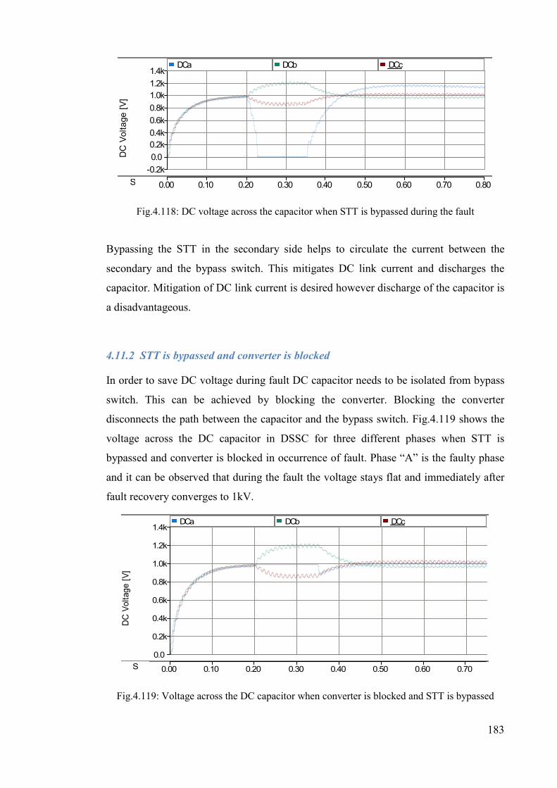
183
Fig.4.118: DC voltage across the capacitor when STT is bypassed during the fault
Bypassing the STT in the secondary side helps to circulate the current between the
secondary and the bypass switch. This mitigates DC link current and discharges the
capacitor. Mitigation of DC link current is desired however discharge of the capacitor is
a disadvantageous.
4.11.2 STT is bypassed and converter is blocked
In order to save DC voltage during fault DC capacitor needs to be isolated from bypass
switch. This can be achieved by blocking the converter. Blocking the converter
disconnects the path between the capacitor and the bypass switch. Fig.4.119 shows the
voltage across the DC capacitor in DSSC for three different phases when STT is
bypassed and converter is blocked in occurrence of fault. Phase “A” is the faulty phase
and it can be observed that during the fault the voltage stays flat and immediately after
fault recovery converges to 1kV.
Fig.4.119: Voltage across the DC capacitor when converter is blocked and STT is bypassed
S 0.00 0.10 0.20 0.30 0.40 0.50 0.60 0.70 0.80
-0.2k
0.0
0.2k
0.4k
0.6k
0.8k
1.0k
1.2k
1.4k
DC Voltage [V]
DCa DCb DCc
S 0.00 0.10 0.20 0.30 0.40 0.50 0.60 0.70
0.0
0.2k
0.4k
0.6k
0.8k
1.0k
1.2k
1.4k
DC Voltage [V]
DCa DCb DCc

184
The injected voltage and line current in the case of bypassing the STT and blocking the
converter is shown in Fig.4.120. It is expected that, injected voltage or line current not
to be affected by blocking converter and bypassing STT. Comparing Fig.4.120and
Fig.4.117 shows that there is no difference in the injected voltage or the line current and
this is satisfying the expectations.
Fig.4.120: Injected voltage and line current when converter is blocked and STT is bypassed
Blocking the converter and bypassing STT in the same time stops current flowing
through the DC link. Fig.4.121 shows DC link current and It can be seen that current is
zero immediately after blocking the converter and it resumes after deblocking.
Fig.4.121: DC link current when converter is blocked and STT is bypassed
S 0.10 0.20 0.30 0.40 0.50
-40
-30
-20
-10
0
10
20
30
40
Injected Voltage [V]
InjVa InjVb InjVc
-1.3k-1.0k-0.8k-0.5k-0.3k0.0 0.3k0.5k0.8k1.0k1.3k
Current [A]
IlineA IlineB IlineC
S 0.00 0.10 0.20 0.30 0.40 0.50 0.60 0.70
-0.150
-0.100
-0.050
0.000
0.050
0.100
0.150
Current [kA]
IDClinkA

185
4.11.3 STT is opened
STT can be open circuit in the secondary side instead of being bypassed in occurrence
of short circuit fault in the power line. In order to take this action a series switch needs
to be located between converter and STT. By opening the switch converter will be
isolated from the STT and consequently from the power line. DC link current shown in
Fig.4.122 falls down below the steady state value and it slowly decays.
Fig.4.122: DC link current when STT is open circuit
Decaying current discharge DC capacitor and reduces the DC voltage. Voltage across
the DC capacitor inside the DSSC device in three different phases is shown in
Fig.4.123. DC voltage in phase “A” decreasing during the fault but it recovers again by
clearing the fault.
Fig.4.123: DC voltage inside DSSC when STT is disconnected from the converter
S 0.050 0.100 0.150 0.200 0.250 0.300 0.350 0.400 0.450 0.500
-0.100
-0.050
0.000
0.050
0.100
Current [kA]
IDClinkA
S 0.00 0.10 0.20 0.30 0.40 0.50 0.60 0.70
0.0
0.2k
0.4k
0.6k
0.8k
1.0k
1.2k
DC Voltage [V]
DCa DCb DCc

186
Disconnecting the STT from the converter makes an open circuit in the secondary side
of STT. Consequently, it inserts series impedance through the line and limits the fault
current even below the steady state value as shown in Fig.4.124. Opening the STT can
be more beneficial as it limits the line short circuit current however, practically it is
impossible to be employed. Opening the circuit induces a high voltage in secondary side
of the STT which can endanger the insulations and related equipments. For this reason
in the presence of fault opening of the STT must be avoided.
Fig.4.124: Injected voltage by DSSC and line current STT is isolated from converter
4.11.4 Converter is blocked
Blocking the converter disconnects DC capacitor from STT and stops converter from
functioning. To achieve this, the control system stops sending firing pulses to the IGBTs
and IGBTs become an open circuit. Current flowing through DC link in steady state and
during the fault is shown in Fig.4.125. It shows that current is increased slightly in one
direction (diodes conducting direction) and id stopped in the reverse direction (diodes
are not conducting).
S 0.00 0.10 0.20 0.30 0.40 0.50 0.60 0.70
-15.0k
-10.0k
-5.0k
0.0
5.0k
10.0k
15.0k
Injected Voltage [V]
InjVa InjVb InjVc
-400
-200
0
200
400
Current [A]
IlineA IlineB IlineC

187
Fig.4.125: Current through DC link when only converter is blocked
In addition, blocking converter means losing control over the voltage across the
secondary of the STT. Consequently, a high voltage will be induced in either side of the
STT (with respect to the turn ratio of the STT they will be different in amplitude) which
as discussed in pervious subsection it can endanger the insulations and equipments.
Injected voltage by STT and line current in three different phases is shown in Fig.4.126.
In this figure the induced voltage is high and it continuously grows but short circuit
current through the line also remains high.
Fig.4.126: Injected voltage by STT and line current in three different phases when only converter is blocked
S 0.00 0.10 0.20 0.30 0.40 0.50 0.60 0.70 0.80 0.90
-2.00
-1.50
-1.00
-0.50
0.00
0.50
1.00
1.50
2.00
Current [kA]
IDClinkA
S 0.100 0.150 0.200 0.250 0.300 0.350 0.400 0.450 0.500
-2.0k
-1.5k
-1.0k
-0.5k
0.0
0.5k
1.0k
1.5k
2.0k
Injected Voltage [V]
InjVa InjVb InjVc
-1.0k
-0.5k
0.0
0.5k
1.0k
Current [A]
IlineA IlineB IlineC

188
Although converter is blocked however DC capacitor still can be charged up through
diodes and as there is no control on the capacitor voltage then it can exceed the limits.
For example, Fig.4.127 shows the voltage across the DC link when converter is
blocked. In this figure capacitor voltage continuously is increasing during the fault and
as soon as the converter is deblocked then voltage start to become under control.
Fig.4.127: Voltage across the DC link when converter is blocked
4.11.5 Concluded fault strategy
During the fault all components need to be protected from high voltage or current. For
this reason different fault recovery strategies have been investigated. For example, when
only converter is blocked DC voltage can exceed the limit which is not desired. In
another scenario, when STT become open circuit -regardless of blocking or deblocking
of converter- there will be high AC voltage in either side of the STT which makes this
solution to be unpractical. Among the examined fault recovery strategies, bypassing the
STT tends to be an acceptable option to be employed. It can avoid inducing a high
voltage in the STT however, it comes with disadvantage of discharging the DC
capacitor. Blocking the converter along with bypassing the STT holds the DC voltage in
pre fault value and avoids a high voltage in the STT in the same time. This is the
solution which is proposed to be taken. Also with this solution, short circuit current
through the faulty line remains unaffected and it is not affecting the fault level of the
power system.
As regard as protecting the switches before detecting the fault and taking the proposed
actions concern, it must be noted that the switches must be rated for the maximum
S 0.0 1.0 2.0 3.0 4.0
-2.0k
0.0
2.0k
4.0k
6.0k
8.0k
10.0k
12.0k
14.0k
16.0k
DC Voltage [V]
DCa DCb DCc

189
possible over-currents and overvoltages. The switches also can be protected against
overvoltages by employing surge arresters in parallel to bypass the switches when the
voltage across them exceeds the maximum withstand voltage. However, the switches
definitely must be rated to the maximum over-current which can occur in the worth
condition.
In addition to the switches components of the LC filter needs to be protected against the
transients. They need to be designed in a way to withstand the worth scenario of over
current and in the same time they need to be protected by surge arresters against the
possible overvoltages.
4.12 Simulation of LC filter
The LC filter is designed to be employed in the experimental tests is simulated in
PSCAD using the selected values of RL in order to observe the performance of the
filter. Having carrier frequency of 1kHz for the PWM pulse generator the output voltage
of the converter, as it can be clearly observed in Fig.4.128 (blue bars), contains high
order harmonics. Some of the major dominant generated harmonics are 18, 20, and 22.
However by using the designed low pass filter the mentioned harmonics have been
eliminated, as it can be seen in Fig.4.128 (black bars). Now only the fundamental
frequency has passed through the filter. In spite of this along with the fundamental
frequency some other low order harmonics with negligible amplitude has been observed
but they are not effective.
Fig.4.128: Harmonics at the input and output of the RLC low pass filter
0
50
100
150
200
250
300
350
400
1 2 3 4 5 6 7 8 9 10 11 12 13 14 15 16 17 18 19 20 21 22
Am
pli
tud
e [
V]
Order of Harmonics

190
Fig.4.129 presents the output of the filter and output voltage of the converter along with
the related PWM switching pattern. This figure shows that the output voltage of the
converter is a chain of pulses with amplitude of ±500 V which are consistent with the
switching pattern generated by the PWM generator. Meanwhile the output of the filter is
a sinusoidal waveform.
Fig.4.129: Output voltage of the filter and converter along with the switching pattern
The output voltage of filter and the output of the converter are also represented in Fig.
4.130 and Fig.4.131 for 5 cycles. The observation of these two waveforms shows the
satisfactory operation of the filter. However it requires a proper tuning of the filter.
Tuning of the filter is a key factor in achieving satisfactory results. The output of the
converter must be carefully monitored and a harmonic analysis must be conducted in
order to have a good evaluation of the existing harmonics. In order to avoid any
resonance and at the same time to eliminate the harmonics, the cut off frequency of the
filter is chosen smaller than the frequency of first dominant harmonic which must be
eliminated. In this study the frequency of first high harmonic is 900 Hz which has order
of 18th and the cut off frequency is set to 112 Hz. The selected cut off frequency is
smaller than the dominant harmonic and will eliminate all the higher harmonics.
Sec 0.100 0.120 0.140 0.160 0.180 0.200 ...
... ...
-500
500
Volt [V]
Output of the filter Output of the converter
0.0
1.50
PWM Signal
PWM

191
Fig. 4.130: Output voltage of the filter
Fig.4.131:Output voltage of the converter
Sec 0.100 0.120 0.140 0.160 0.180 0.200 ...
... ...
-600
-400
-200
0
200
400
600
Volt [V]
Output of the filter
Sec 0.100 0.120 0.140 ...
... ...
-500
-400
-300
-200
-100
0
100
200
300
400
500
Volt [V]
Output of the converter

192
4.13 Summary
In this chapter, in order to avoid using dq conversion and provide a compensation which
is independent from line current a new closed-loop control strategy based on the
exchange of instantaneous power is proposed. The control guarantees an orthogonal
injection of voltage with respect to the line current. It also optimizes the active power
absorption by the DSSC device and holds the DC voltage at desired value at the same
time.
The DSSC device was modelled by dividing its modes of operation into two categories.
In mode 1 IGBT’s 1 and 4 within the DSSC device are conducting and IGBT’s 2 and 3
are off. In mode 2 IGBT’s 1 and 4 are switched off and IGBT’s 2 and 3 are conducting.
Based on these two modes of operation and considering equivalent impedance of the
system in each mode, transfer function of system was obtained.
The obtained transfer function is used in designing of a controller. The controller
stabilizes system by inserting zeros and the proper location of the zeros are found using
SISTOOLS of MATLAB. Stability study is conducted using step response of the closed
loop system when the designed controller is employed. In addition, effect of change of
system parameters on the performance of the designed controller has been investigated.
Change of system parameters includes change in the capacitance of DC capacitor, AC
capacitor (filter capacitor) and inductance of filter. These parameters do not put stability
of system at risk as long as their changes are limited to 10%. In sensitivity analysis,
effect of adding a low pass filter to the proposed controller was investigated. Bode
diagram of filter was plotted and it has been observed that filter does not have any
attenuation or phase delay in the DC and the data which is being used by controller is in
the DC.
The performance of the DSSC and the proposed controller has been studied using
PSCAD. This study employs, an 11kV distribution network comprised of two parallel
lines are connected to an 11kV substation at one end and supplying a lumped load at
another end. The amount of compensation as a percentage of line reactance can be
determined by adjusting the amplitude of the injected voltage. This study has
demonstrated that the applied control system is capable of injecting both capacitive and
inductive reactances through the line.
In comparison with 90° phase shift approach the proposed controller has managed to
reduce the phase angle difference of injected voltage with respect to the line current. In
the same time reduces the level of injected harmonics through the line by DSSC when

193
proposed controller has been used.
Comparison of performance of the proposed controller with dq based controller
demonstrates independency of the proposed controller from the unbalance currents of
three phase power system. Reference signal in the dq based controller is affected and
their amplitude are not same. Then DSSC device can provide compensation which is
differed from the demand. However, proposed controller shows that regardless of
unbalance current and voltages in the three phase system, DSSC is able to inject same
voltages in each phase as per demand.
The proposed controller in comparison with the controller which is using only DC link
voltage regulator demonstrates better performance with respect of injection angle. When
only DC voltage regulator has been used the injection angle is diverting from the target
(90°) and it is oscillating. Diversion from the target angle means the capacitive or
inductive injection is not purely reached.
Sensitivity of controller with respect to the change of power system parameters has been
studied. This study includes power system parameters changes such as line resistance,
voltage sag swell and reconfiguration of the network. The results show satisfactory
performance of controller in injection of the series voltage through the line and
regulating of the DC voltage.
A fault management study has been conducted in order to find best fault recovery
solution in occurrence of fault within the system. When only converter (within the
DSSC) is blocked DC voltage can exceed the limit which is not desired. In another
scenario, when STT become open circuit -regardless of blocking or deblocking of
converter- there will be high AC voltage in either side of the STT which makes this
solution to be unpractical. Blocking the converter along with bypassing the STT holds
the DC voltage in pre fault value and avoids a high voltage in the STT in the same time.

194
5 Experimental Results
Although the proposed control and its performance is well simulated using
PSCAD/EMTDC, however, a laboratory test bench is needed in order to conduct
experimental tests and validate the simulation results. To do so, based on the available
lab facilities in the Upper Ground (UG) lab at Newcastle University, a low voltage test
bench is designed and implemented. The overview of the test bench is shown in Fig.5.1.
As can be seen, it includes DSSC device and low voltage power system.
Fig.5.1: The overview of the inside of the test rig
The power circuit of the DSSC device comprises of a voltage source H-bridge converter
(VSC), a single turn transformer, a DC capacitor serving as a DC link, an LC filter. The
control electronics is digitally implemented using dsPIC33F microcontroller, electronic
measurement, control boards and a DC power supply. In this device, a 500µF capacitor,
rated at 1.5 kV is used as a DC link to hold the DC voltage provided by the converter.
Converter itself is a full H-bridge IGBT module, which is connected between DC link
and LC filter. The LC filter is located between the converter and a single turn
transformer. It is built up of a capacitor and an inductor. The filter is a low pass filter,
designed to eliminate high order harmonics generated by the converter. As a result, it
can provide a non-distorted sinusoidal waveform at the secondary of the STT.
The single turn transformer is a cylindrical shape transformer. Its primary winding has
just one turn and it is the power line itself. In the compensated electrical networks it is
supposed to be suspended from the lines.
The dsPIC33F microcontroller is used to process the incoming signal from the system
and to run the control algorithms. The incoming feedback signals from the system, have
been provided by the electronic measurement boards. Also another electronic board has
been designed serving as an interface between the output signals from the controller and
the converter.

195
The 11 kV power distribution feeder is modelled by a 50 volts power system. This low
voltage is chosen according to the maximum voltage permissible by the rules and
regulation of health and safety in the UG lab. The system comprises of a 30mH inductor
representing the inductance of the line and in series with a 6 Ohm resistance
demonstrating the ohmic resistance of the line. The power system is supplied by a
220:50 transformer with a maximum current of 15A. The galvanic isolation between the
test rig and the main power supply in the lab is achieved by supplying the 220:50
transformer with a unity-ratio isolation transformer. This will protect the main power
supply in the lab from any probable fault which may occur during the experimental
tests.
The power system as shown in Fig.5.1 is a single phase line and there is only one DSSC
device connected in series with it. At the end of the line there is a load through which
the line current is passing. Also, in order to demonstrate that the DSSC module is
operating correctly, contributing toward the power flow control in the system, there
must be another parallel line to supply the load. This extra parallel line will facilitate
this by changing the reactance in the compensated line to be able to change the amount
of current passing through the compensated line and consequently in the parallel line.
For this reason another parallel line, exactly with the same characteristics as the first
one is also provided in the test rig. As stated earlier, the parallel line will only be used in
the power flow control test.
Having designed and built of the test rig the proposed control strategy implemented on
the microcontroller and it is executed to conduct experimental tests to validate the
simulation results. The capability of control system in generating capacitive and
inductive injected voltage is examined in this chapter. In addition its efficiency is
compared with the traditional control method.
5.1 H-Bridge Voltage Source Converter
The main power electronics device in the DSSC unit is the H-bridge voltage source
converter. The converter as shown in the Fig.5.2 comprises of four IGBT and four anti-
parallel diodes. The dc side of the converter is connected to the DC capacitor, whereas
the AC connection points are connected to the LC filter. The maximum current passing
through (when IGBT is conducting) and the maximum continuous voltage across the
IGBT (when it is off) needs to be considered carefully. In the same time its power rating
is also important parameter in the selection of IGBT.

196
The selected DC capacitor is rated at 1.5 kV, therefore in the worst case the maximum
voltage of the DC link will be controlled not exceeding 1.5 kV. For this reason the
maximum continuous voltage across each IGBT will not exceed 0.75 kV in steady state.
However, Transient Over Voltage (TOV) can be higher. Regarding to the rated current,
the nominal current of the 220:50transformer connected to the power system is 15A. As
a result the resistors including the connected load to the system has the same range of
nominal current. The current in the secondary side of single turn transformer depends on
the turn ratio of the STT, let say n, and it will be n times smaller than line current. It is
obvious that normally n is a number between 1 and 100 and that the current in the
secondary side, not only cannot exceed 15A, but also it will be much less than current in
the primary side.
Another important factor in the selection of IGBT in the design process is the IC
(collector current of IGBT) versus VCE (voltage across the collector-emitter of the
IGBT) curve for different VGE (voltage across the Gate-Emitter). This curve normally is
provided by the manufacturer and it is shown and explained in appendix B [91].
Fig.5.2: H-bridge voltage source converter
In the design of DSSC device, based on the aforementioned ratings for voltage and
current, the IGBT module SK20GH123, manufactured by Semikron, is chosen for
building up the converter used in the DSSC.
It can be deducted from ICE-VCE curve which is well explained in appendix B that the
IGBT can initiate a current flow even with VGE=7 volts but the current will not exceed
3A. For this reason and in order to reach the rated current flow, high VGE is required.
In order to meet all these requirements in the design of gate driver board, the turn-on
voltage for the IGBT’s inside the SK20GH123 device is set to 15 volts. Additionally, a
negative gate voltage is required to turn off the switch and provide immunity against

197
dv/dt. The lowest range of turn-off voltage for the selected IGBT is -20 V. However
lower gate voltages, similar to higher turn-on gate voltage, can cause a permanent
damage to the device and at the same time low negative gate voltage can be problematic
as well. Because there is a series resistance inside the gate of IGBT and low gate
voltage can lead to a slow switching.
In order to turn on the IGBT and let current flows from the collector to the emitter there
must be a positive voltage across the collector-emitter and gate-emitter terminals.
Referring to the data sheet [91] of the selected IGBT, VGE (th) is in the range of 4.5 V -
6.5 V and the typical voltage is 5.5 volts. Moreover the details of gate leakage current
and other parameters in general and especially for the selected IGBT can be found in
[91] and appendix B. The IGBT cannot be turned on or off directly by the controller
itself, hence there must be buffering interface between them. The interface board, not
only provides proper voltage and current to drive the IGBT, but also isolates the power
switches, IGBT’s, electrically from the microcontroller.
5.2 Gate Driver Board
Gate driver board is mainly employed to convert control signals such as switching
pattern to a proper voltage or current in order to turn on or off the IGBTs. At its output,
it must provide the required turn on or turn off energy for the related IGBT. To do so,
the outer level power supply and the series resistor (gate resistor) must be chosen
carefully in order to provide a current with proper amplitude to charge or discharge the
IGBT with minimum possible time. A gate driver board is composed of two different
parts and a typical plan of this board is shown in Fig.5.3. The first part is called Buffer
which is directly connected to the microcontroller and the second part is called Gate
Drive and is located between buffer and IGBT. Four buffers provide the required
current for the gate drive, otherwise it is not possible for the microcontroller itself to
feed all of the gate drives.

198
Fig.5.3: Typical layout of Gate Drive Board
In order to guarantee high impedance between microcontroller and the gate driver a
proper buffer is required to avoid sinking too much current from the microcontroller. To
do so, based on the output voltage of the microcontroller, 5 volts, and input voltage of
the gate drive, 5 volts, the chip SN74AHCT125N is selected for its current sinking
capability [92]. Also it is compatible with a supply voltage of 5 V which can easily be
provided by many of the ordinary DC power supplies and will avoid a need for special
DC source.
In [93] the range of supply voltage is specified between 0.5 and 7 volts however the
recommended supply voltage is given between 4.5 V and 5.5 V. For this reason, VCC, is
defined to be 5 volts.
Another important component in the gate drive board is gate driver. It provides the turn-
on and turn-off voltages directly. In most of the designs for IGBT, it also provides the
adequate amount of power to charge and discharge the gate of IGBT. Additionally, gate
drive must isolate the signal level from the power circuits and usually this can be
achieved by an integrated opto-coupler within the gate drive. It must be well-matched
with the carrier frequency of PWM pulse generator in order to transfer the generated
signals to power converter and to be fast enough to correspond to the changes in the
input. Some electrical features such as input and output voltages and currents must be
compatible with the related parameters in the connected device.
For example when output voltages of the bufferSN74AHCT125N, is 5 V and its output
is an input to the gate drive, then the input of the selected gate drive needs to be 5 Volts.
Similarly, the input current of the selected device must not exceed the 12 mA limit

199
which is the designed output current for the buffer as explained earlier in part 6.3.1. In
addition, the PWM signal frequency depends on the different test scenarios and is
expected to vary between 1 KHz and 10 KHz and the gate drive must have enough
bandwidth to deal with the generated signals.
It is also required that the supply voltage feeding the device can easily be provided by
normal DC power supplies. Based on all of the aforementioned requirements, the opto-
coupler HCPL-3180 device is selected. Its features and further technical data can be
found in Appendix B.
However gate drive (gate drive component) needs an “isolated power supply” in order
to provide the required voltage for turn-on and turn-off of the IGBT. It is like a DC
power supply which can provide voltage and reference ground. This is because firstly
the output voltage of the gate drive is less than 15 V and this will not be able to force
IGBT to conduct fully. Then there is a possibility that the flow of current through the
device not to reach the rated current. Secondly, in the H-bridge converter two IGBTs
(IGBTtop and IGBTbot) are connected in series in such a way that the emitter of top
IGBT is connected to the collector of the bottom IGBT. For this reason the voltage of
emitter will be depend on the ON or OFF status of the bottom IGBT. In order to avoid
floating voltage across the gate-emitter, the use of an independent power supply is
necessary to guarantee the required voltage across the gate-emitter.
Based on the electrical requirements specified in the appendix B in terms of input,
output currents and voltages, the NMF0515S isolated power supply is selected to be
employed in the board. It converts 5 volts at the input to 15 volts at the output. Since the
isolated power supply is a DC/DC converter and is connected to the power circuit, it
must have sufficient insulation for high voltages in order to operate safely in such
voltages. Additionally, it is necessary that the selected device has enough isolation
capacitance in order to avoid any dv/dt issue. The NMF0515S power supply, the
selected device, is isolated for 1000 V, which is much higher than the expected DC
voltage across the DC link in the converter [94].
Another important consideration in the design is the maximum peak gate current. Refer
to appendix B and data sheet of selected component [94] the gate current must not
exceed 2.5 A; however practically because of negligible impedance of output circuit of
the gate drive it is not possible. Therefore, the current must be controlled by adding a
series resistor between the gate drive and IGBT. The resistance can be calculated as
follow:

200
RÖ = ∆Þ±ßà (5.1)
where RG is the resistance of series resistor between the gate drive and IGBT, Ipeak is
the maximum peak output current of gate drive. The ∆V represents the variation of the
required gate-emitter voltage for turning on and off of the IGBT. For the
SN74AHCT125N the maximum output current is 2.5A and for the IGBT the ∆V is 30V.
Therefore:
RÖ = 302.5 = 12Ω RG, under any conditions, must not be smaller than 12 Ω otherwise the peak current will
exceed the permissible output current of gate drive. However, practically the impedance
of the gate drive circuit is not zero and it will contribute toward the RG and the peak
current will be less than 2.5 A. Furthermore this current will decay as the gate
capacitance in the IGBT charges up. But the value of peak current is a key factor in
charging up time of the gate circuit in the IGBT. This is because with higher peak
current the charge up time will be less and this will increase the efficiency of the
switching and will reduce the switching power losses. This is because with smaller
resistor the gate capacitance will charge and discharge quickly and switching will take
less time.
On the other hand, the smaller external resistor will increase the immunity against the
dv/dt in the gate circuit. However smaller value of external resistor can increase di/dt
stress through the free wheel diodes in the converters which are connected to an
inductive loads. This can create a transient over voltage across the switches also it can
generate an oscillation. In order to solve this problem, a higher external resistor value is
required but it will increase the switching losses. In each switching event current flows
through the resistor and increasing the resistance will increase the losses. For this reason
sometimes having two different external resistances, one for charging the gate
capacitance in the IGBT and the other one to discharge the gate capacitance are used. In
order to have two different external resistors the gate drive itself must have two
different outputs but this can increase the complexity of design and implementation of
the gate drive board which is not necessary in most of the cases. Especially when the
switching frequency is quite low then there is no need to have separate charge and
discharge gate circuits.

201
5.2.1 Design of gate drive board
Detail of the design is presented in Fig.5.4 and it can be clearly observed that the input
signals are first fed into the buffer, SN74AHCT125. Then the related output signals are
connected to four gate drives, HCPL-3180, via series resistors and the resistors are
controlling the current flowing between buffer and gate drive. The gate drives are
supplied by isolated power supply, NMF0515S, and they operate like a DC-DC
converter and always provide a fixed voltage of 15V volts between P3 and P5.
This voltage appears at the output of gate drive, between pins 8 & 6 or between 5 & 6,
and provides the gate-emitter voltage via a series resistor.
Fig.5.4: Design of the gate drive board
5.3 Voltage Measurement Board
Generally measurement is a key factor in the control systems especially when the
measured parameters are used as feedback signals in the control blocks. The capability
and performance of the controller can be affected by accuracy of the measurement. In
the proposed control strategy, instantaneous value of DC voltage and injected AC
voltage are two important inputs along with the instantaneous line current for the
controller.
To provide these two voltage inputs for the controller two voltage measurements have
been designed and implemented. The voltage measurement board includes two main

202
different parts. The first part is a voltage transducer (VT) which is connected in the
primary side in parallel with the target points to measure the potential between them.
The second part is a combination of op-amp circuits that are providing desirable signal
to the microcontroller. The selection of the VT depends on the expected maximum and
minimum voltage between the points that VT will be connected and also the accuracy of
measurement which is demanded by the control system.
Each VT, like any electrical equipment, has rated values for certain input and output
voltage and current which specified by the manufacturer. In the same time the
mentioned parameters must be matched with the expected measured voltages. For
example the DC voltage across the DC link and AC voltage across the secondary side of
the single turn transformer (STT) in the laboratory prototype DSSC module is not
expected to exceed 500 volts (however the employed capacitor is rated up to 1.5kV in
order to withstand to transient over voltages). For this reason, in the voltage
measurement board design the nominal primary voltage is planned to be 500 volts.
Based on the design requirements and the available VT in the market and having
considered their accuracy, the voltage transducer LV 25-P has been selected [95].
Refer to the device data sheet [95] and appendix B the optimum accuracy of the device
can be achieved if the primary input current in the measuring of the nominal voltage
become 10 mA. In order to obtain such accuracy in our design the external resistors in
DC voltage measurement board and AC voltage measurement board have been selected
so that when measuring 500 V and 200 V respectively the corresponding currents to be
10 mA. To do so, Re the external resistor, can be calculated as follow:
RG = ÞãÞã (5.2)
In equation (5.2) VPN is the measured voltage and IPN is the primary current in the input
of transducer. Considering the maximum peak value of injected voltage by DSSC in the
prototype system, the voltage is expected to not exceed 200 volts in the power
electronic side. This is the voltage that needs to be measured by AC voltage
measurement then the VPN in this board is 200 volts. For example, with substituting this
value and 10 mA as input current in equation (6.2), Re is calculated as follow:
RG = 200V10mA = 20kΩ Re is selected to be 20kΩ and similar calculation can be done for Reused in DC voltage
measurement board. In this board the nominal measured voltage is assumed to be 500V
then the Re is calculated to be 50kΩ. Then with having 20kΩ and 50kΩ resistance at the

203
input of the VT the accuracy of the measurement refer to appendix B will be 0.8 % in
both boards.
Another element which is used more frequently in both DC and AC voltage
measurements is Operational amplifier (Op-amp).In order to alter some electrical
features of measured signals using specified circuits and provide the desired electrical
signals. However care must be taken in selection of Op_amp because a device with poor
slew rate can generate a nonlinear effect in the circuit. For this reason especially in the
measurement circuits design the slew rate of the employed devices becomes more
important because any nonlinearity in the measurements can cause instability in the
system. In the voltage measurement board, the LMC660CM is selected to be used in the
design. Because typical slew rate of the LMC660CM is 1.1 V/µs; however refer to the
data sheet of the device [96] and appendix B a minimum slew rate of 0.8 V/µs is
guaranteed at the ambient temperature.
5.3.1 Design of voltage measurement board
The voltage measurement board includes electronics circuits and a voltage transducer
(VT). VT is located between the electronics part and power circuit and isolates these
two parts electrically. As a part of the design process an external resistor needs to be
used to limit the input current which is explained earlier in pervious subsection. By
having 10mA input current the output current of the VT, considering the turn ratio of
2500:1000, will be 25mA. Considering Kirchhoff Current Law at the output of the VT
the KCL equation can be written as follow: iå = i? + iÉ (5.3)
where iO is the output current of VT and i1 and i4 are the current passing through R1 and
R4 in Fig. 5.5.It is noted that i1 is almost negligible because the input impedance of the
op-amp is high and in ideal condition the current passing through it is zero. Substituting
i1 equal to zero in equation (6.3) it can be concluded that: iå = 0 + iÉ iå = iÉ It means that the output current of the VT wholly passes through the R4. As a result
there will be a voltage drop across the R4 which can be calculated as follow: vå = iÉ ∗ RÉ (5.4)
Using the corresponding values VO can be found as follow:
vO= 25 mA * 100 Ω= 2.5 V

204
In the circuit the output of the VT is connected to a low pass filter which can smooth the
measured signal by bypassing the high frequency signals. The gain for the low pass
filter can be written as follow:
våç = −v ∥w~w (5.5)
where VOut and Vin are the output and input of the filter, Xc1 is the reactance of the
capacitor. As the frequency of the input signal goes high then the reactance of the
capacitor will go to the zero and then the gain will be zero. When the frequency of the
signal goes down the reactance of the capacitor will go high and then only R2 will affect
the gain. So, for the low frequency signals the gain will be:
våç = −v w~w (5.6)
As it can be clearly observed from equations (5.5) and (5.6) the designed low pass filter
is inverting (180 degree phase displacement) the signal as well. Therefore the signal
needs to be inverted once again in order to return it back to the original phase. In the
same as the measured voltage is an AC voltage then it has positive and negative
amplitude repeatedly during each cycle. However the microcontroller requires a positive
signal between 0V and 3.3 volts. In order to meet these conditions the final signal must
vary between the mentioned voltage bands. To do so, after low pass filter circuit another
circuit is needed while inverting the signal gives the required offset and adjust the
amplitude of the final signal. For this reason an inverting op-amp circuit along with the
offset bias circuit is added immediately after low pas filter circuit in this design.
However there could be other solutions which can avoid using multiple Op-amp
circuits. The bias circuit is just adding up some value on top of the signal in order to
guarantee that the final signal will not go to negative. The added value can be calculated
as follow:
vé = ∗wÌwê#wÌ (5.7)
where Vbias is the added value. Substituting the corresponding values into equation (5.7)
the Vbias can be calculated as follow:
vé = ?%∗??K#?= 0.85 However gain of the inverting Op-amp circuit along with Vbias is:
våç = −v wëwÍ + 0.85 (5.8)
and substituting the corresponding values, VOut can be calculated as follow:
våç = −v 10k10k + 0.85 = −v + 0.85

205
After this op-amp circuit there are two protective diodes which they are connected
between final output and ground and a node with potential of 3.3 volts. The aim is that
if with any reason the amplitude of output signal becomes less than 0 V or greater than
3.3 V then the related diode will conduct and consequently the microcontroller will be
protected. All of the aforementioned circuits can be seen in the Fig. 5.5. This figure
shows the design of voltage measurement board which is obtained using Multisim
software.
Fig. 5.5: Design of Voltage Measurement Board
5.4 Current Measurement
Current measurement board is used to monitor current waveform through the power
line. As the DSSC current is linked to the power line current via a single turn
transformer then the monitored current waveform includes the instantaneous
information of the current inside DSSC as well. However based on the proposed control
strategy the injected voltage must be in orthogonal with the line current. For this reason,
the line current itself is directly monitored and fed to the microcontroller so that it can
be used by control algorithm.
The accuracy and precision of the current measurement board becomes more important
which must be considered in the design process of the board. It comprises of a Current
Transducer (CT) and an electronic circuit. The CT is fed by the measured current and
provides a voltage type signal at the output. This voltage is fed to the electronic circuit
and the circuit provides a proper signal at the output.
One of the major criteria in the selection of CT is the maximum primary current that CT
can take at the input. However in the designed prototype test rig based on the UG lab

206
facilities, the maximum current in the power line will be 15 A then in terms of the
maximum input current any CT with input current above 15 A will be fine. In terms of
required supply voltage of CT, it is desirable to be in the standard voltage range then it
can be easily provided by the standard DC power supplies. Also, it is required that the
selected CT be mountable on the PCB board in order to facilitate its employment along
with the electronic board within one PCB board.
The most important feature of CT is its accuracy as it can affect the proper operation of
control system. Considering all the aforementioned futures the LTS 25-NP Current
Transducer has been selected for the current measurement board. More information
regarding the selected CT and check against the required design criteria can be found in
the appendix B.
The selected CT has capability of measuring current of up to 25 A which is enough for
our purposes [97]. Also it requires 5 volts as supply voltages which can be provided by
most of ordinary standard DC power supplies.
The output voltage can be defined as [72]: Vç = 2.5 ± (0.625 ∗ I Ií)V⁄ (5.9)
where Vout is the output voltage and IP and IPN are the primary current and nominal
primary currents, respectively. The current measurement board is designed for nominal
current of 25 A then by substituting IPN with 25 A the equation (5.9) can be rewritten as: Vç = 2.5 ± (0.025 ∗ I)V (5.10)
From equation (5.10), it can be clearly argued that the output voltage has offset of 2.5V.
That means even with zero input current the output voltage is 2.5 volts and it must be
considered in the design.
5.4.1 Design of electronic circuit of current measurement board
Electronic circuit of the current measurement board comprises of different op-amp
circuit which are in cascade connection. The first part, as shown in Fig.5.6, is a Non-
Inverting Amplifier. It is the first point of connection to the CT. As explained in section
5.4 the output voltage of the CT includes 2.5V DC voltage and it must be bypassed in
order to pass the alternating part of the output voltage. Actually only the alternating part
of the voltage includes information about the measured current for this capacitor C1 is
located between the Op-amp circuit and CT and it bypasses the DC voltage.

207
Fig.5.6: Non-Inverting Amplifier
The output voltage of the amplifier, shown in Fig.5.6, can be calculated as
Vå? = w~#wïw~ ∗ V (5.11)
where VO1 is the output voltage of the amplifier and Vin is the input voltage.
Substituting R2 and R3 in equation (5.11) with 4.4kΩ and 13kΩ the equation (5.11) can
be rewritten as Vå? = 3.95 ∗ V (5.12)
Equation (5.12) shows that the gain of amplifier is 3.95. Considering the input voltage
margin of 0.375 V for the maximum input current of 15 A the VOut will be 1.48 V.
It means that VO1 will vary between -1.48V and 1.48V. However the negative voltages
are out of the acceptable input voltage margin of the microcontroller. In order to bring
signal into the acceptable margin some other op-amp circuit are required. The complete
electronic circuit of the current measurement board is shown in Fig.5.7. In this circuit,
after the Non-Inverting Amplifier there are two cascaded Inverting Amplifiers. The first
one is just inverting the signal and the relation between its output and input can be
written as
Vå% = − wÍwÈ V% (5.13)
where Vi2 and VO2 are the input and output of the first inverting amplifier. Equation
(5.13) is a general formula, thus it can be applied to all inverting amplifier circuits. With
substituting values of R5 and R4 into (5.13) it can be rewritten as Vå% = −V% (5.14)
The second inverting amplifier includes some DC offset while it is inverting the signal.
The relation between its output and input can be written as

208
VK = wñwë VK + Vò (5.15)
where Vi3 and VO3 are the input and output of the second inverting amplifier circuit and
VDC is the DC offset. The DC offset is just shifting up the signal in order to avoid
appearing any negative signal at final output of the measurement board. VDC is provided
by a voltage divider and can be calculated as
Vò = wêwê#wÌ ∗ 12 (5.16)
Substituting the values of R8 and R7 into equation (5.16) the VDC becomes 1.6V. In
continue in equation (5.15) by replacing the values of R9 and R6 and VDC it will
become VK = −VK + 1.6 (5.17)
It is argued earlier that the VO1 will vary between -1.48 and +1.48 then by using these
values in VO2 and VO3 the final output VO will be as Vå = ±1.48 + 1.6 (5.18) Vå = 3.1OrVå = 0.1 (5.19)
Based on equation (5.19) the final output voltage of the measurement board is located in
the permissible margin of the input voltage of the controller, which is between 0 V and
3.33 Volts. However a protection for the microcontroller input is needed just in case the
output voltage goes beyond the safe margin. To do so, two diodes are connected the
output and they will conduct if the output voltage become more than 3.2 V or less than -
0.6 V. In the former D1 and in the latter D2 will conduct.
Fig.5.7:Full circuit of the current measurement board

209
5.5 Single Turn Transformer (STT)
Single turn transformer mainly consists of a cylindrical core and a secondary winding.
The primary winding is the power line itself which is passing through the cylindrical
core. The core is made of two parts, clamped to each other to make a complete cylinder.
This makes the mounting and dismounting of device to be simple. However in the
practical design there is an air gap between the parts and will be included in the
magnetic path of the flux.
The secondary winding is wound on the core, as shown in Fig.5.8. This winding is
coupled to power line like a conventional transformer. As the current flowing through
the power line it induces current in the secondary winding. However the induced current
is much lower than the line current. Actually it is reduced by the turn ratio of
transformer, let say 1:100, and even in the case of short circuit just small proportion of
current can pass through the power electronic circuits before bypassing the STT in the
secondary side by mechanical switches.
Fig.5.8: Single Turn Transformer
The STT can operate in two different modes of functionality. First mode of operation
occurs when the secondary side is bypassed by a mechanical switch. By shortening the
secondary side secondary voltage will be zero and the induced voltage at the primary
will be zero. In this case, there is no injection in the primary side except the injection of
leakage inductance which is negligible and has no effect on the proper operation of the
power system. In the second mode of operation, the secondary winding is connected to
the converter via a low pass filter and the generated voltage by the H-bridge converter is
injected by STT. Because the injected voltage can lead or lag the line current then as a
result of injection inductive or capacitive reactance can be induced through the line.
The maximum reactance which DSSC can be injected through the power line depends
on the magnetizing inductance, X, of the STT. The magnetizing inductance is equal to
the self-inductance of the power line (or primary winding) and is related to the
reluctance of the core of STT. In cylindrical core distribution of the air gap between

210
line and core is identical around line and reluctance in different points of the core can be
calculated as follow:
ℛ = %õö(∗6) (5.20)
In equation (5.20), r is the thickness of the core as shown in Fig. 5.9 and r1 is the
distance of the calculated point from the centre of the cylinder. In this equation, l is the
length of the cylinder and µ is representing the permeability of the material of the core.
The reluctance of magnetic path in the core is highly dependent on the permeability of
the material. For this reason by introducing air gap in the magnetic path the reluctance
can be increased. Air gap in magnetic path of STT is unavoidable and it has been
introduced by gap between the two parts of the core. These two parts are clamped to
each other in order to create a circulation path for the flux. However increasing the
reluctance of the magnetic path in presence of air gap is desirable. Because in the
transmission and distribution lines the flowing current can be very high and
consequently the core can be easily saturated which can affect the proper operation of
the DSSC.
Fig.5.9: Cross section of the STT core
By creating an air gap the magnetizing inductance of STT can be tuned to the desirable
value. In spite of this, in the design of laboratory prototype model of STT the air gap is
not considered. Because it is used only in the laboratory test rig and there is no need of
to be made of two parts in order to ease off the mounting and dismounting the device
through the power line. Additionally, as the applied current in the power system in the
test rig is considerably low and will not exceed 15A then with the intention of
increasing flux density in the core the STT is made of just one cylindrical core.
However, full design steps of the single turn transformer that can be used for an 11kV
distribution network is explained later in this chapter.
The connection of DSSC device and relations between the current and voltages are
shown in Fig.5.10.

211
a) STT is injecting a voltage source through the line
b) Relation between the voltages in a compensated power system
Fig.5.10: The connection of DSSC device and relations between the current and voltages
The maximum voltage that STT can inject highly depends on the design of its magnetic
core. The magnetic permeability of core must be high enough in order to provide proper
reluctance for the generated magnetic flux by the power line. This will increase the
coupling of the transformer and efficiency of the device. The core chosen is made of
non-oriented silicon steel laminations, which is called M33035A, with maximum flux
density of B= 1.5 T.
The induced voltage by single turn transformer can be calculated as follow: V)*+ = 4.44BøANf (5.21)
where Vinj is the injected voltage and Bø is the flux density in the core. Also A is representing the net cross-sectional area of the core and N is the number of turns of the
winding around the core. In this equation, f is the frequency of the injected voltage and
it is same frequency of the line current which is equal to 50 Hz. To induce 6V, VInj=6 V
(fundamental), in the primary side with substituting B= 1.2 T, f=50 Hz and N=1 in
equation (5.21) the cross sectional area for the STT, A, can be calculated as
A = 64.44 ∗ 1.2 ∗ 50 = 0.0225m% In order to meet the cross sectional area of A=0.0225 m2 one of the possible options is
using value of r= 0.075 m and l= 0.3 m as represented in the Fig.5.11 and can be
calculated by equation (5.22).

212
A = r ∗ l (5.22)
Fig.5.11: Core of STT
However, the thickness, r, and length, l, of the core can be different values but at the end
the required cross sectional area must be provided. In the same time volume of cylinder
should bare minimum in order to minimize its weight. Having considered this in the
final design, r is chosen to be 0.06 m and l is decided to be 0.3 m. With having these
values the related cross sectional area is calculated to 0.018 m2. So in order to induce 6
V in the primary side with the calculated A= 0.018 m2 the required flux density can be
calculated using equation (5.21) as follow:
Bø = 64.44 ∗ 0.018 ∗ 1 ∗ 50 = 1.5T The calculated flux density, 1.5 T, is in the margin of magnetic saturation of the
employed magnetic lamination in the core. Moreover, B=1.5 T, will be required when
the injected voltage is expected to be 6 V however in the experimental studies using the
implemented test rig the injected voltage will not reach to 6 V. Then the saturation of
the core is guaranteed because of lower than 6 V injected voltages.
The magnetic field strength in the core, H, depends on the magnetic permeability of the
material which the core is made of and the flux density in the core. The relationship
between the field strength and flux density can be written as follow:
H = üøö (5.23)
where H is the magnetic field strength, B is the flux density and µ is the magnetic
permeability.
On the other hand, magnetic field strength in the different distances from the centre of
the core is different and it decreases by increasing the distance. However, H also has a
relationship with the magnitude of electrical current flowing through the wire in centre
of the core as well. In this case by increasing the current the H is increasing as well. H
can be formulated as

213
H = í´µ6 (5.24)
where Il is the magnitude of current flowing through the power line and N is the number
of turns in the primary winding. In this equation, l is representing the length of distance
that magnetic flux needs in order to close the loop. For example at the distance of 0.04
m from the core centre the length is equal to 2*π*0.04= 0.25 m. For the selected core
material µ is approximately equal to 0.015 and for the designed core B=1.5 T and with
substituting these values in the equation (5.23) H can be calculated as follow: H = .Íý.ýÍ = 100 With substituting H=100, l=0.25 and N=1 in the equation (5.24) the required current for
generating flux density of 1.5 T in the distance of 0.4 from the centre of the core can be
calculated as follow:
I = H ∗ lN = 100 ∗ 0.251 = 25A It can be concluded that the designed core for injecting 6 V in the primary side needs 25
A current passing through the centre of the core. However practically through the
experimental studies the injected voltage is not exceed 2 V. Because, first of all from
the health and safety regulations of the UG lab the secondary side voltage must not
exceed 50 V and with considering high turn ratio of the STT, 1: 25, the primary side
voltage can be restricted to 2 V or less. Secondly, because of low rated facilities of the
UG lab such as supply transformer and even reactance and load practically it is not
possible to exceed 15 A current in the power system in the test rig. Then, although the
designed single turn transformer has capability to inject 6 V in the primary side through
the power line but practically because of the aforementioned restrictions the injected
voltage is not reached to the nominal value.
The designed STT consists of secondary winding. However this winding is not a fixed
winding and can be easily replaced by another winding with different turns in order to
provide injected voltages with different voltage magnitude. For example, through the
experimental tests the turn ratios of 1:25, 1: 50 and 1:75 have been used in different test
scenarios. All the windings are wounded around the designed core which has 30 cm
length. By dividing the length of cylinder (30cm) with the thickness of each laminate
(5mm) the required numbers of laminates obtains 600. The core is built up by stacking
600 laminations of M33035A with thickness of 0.5mm together in order to provide the
required length of 30 cm. The laminations are bolted to each other in three different
points. The location of bolts in the cross section of core is shown in Fig.5.12.

214
Fig.5.12: The location of bolts in the cross section of core
The holes in three different locations are made far from the centre of the core with
intention of saving the material close the centre. The density of flux close to the centre
is higher than that in the outer layer of the core. Therefore losing the material in the
centre can lead to early saturation of core. The laminations are made of non-oriented
silicon steel which has same magnetic property in all direction. This reduces the flux
density in the core but it must be noted there is no air gap in the design and this will
help to avoid the magnetic saturation of the core.
In the oriented silicon steel the magnetic properties are in one direction and if it matches
with the direction of flux then the flux density can increase. However if this kind of
lamination is used then the air gap and having two part core is recommended.
Otherwise, as the permeability of the core is much higher than the air then the flux will
concentrate through the core rather than the air path. Both the air and magnetic paths are
in parallel and of course the flux will pass through the way that has low magnetic
resistance. But if there is an air gap between the two parts of the core then the reluctance
of air gap will be in series with the reluctance of the core and consequently the resultant
reluctance will be higher than reluctance of pure magnetic path of one part core.
5.6 Design steps of single turn transformer to be employed in an 11kV
distribution feeder
Line parameters of a typical overhead line (employed in an 11kV distribution network)
are tabulated in Table 5.1[77]. Design of STT can be customised for specific
requirements. For example in this design, DSSC is assumed to compensate 10% of line
reactance. In order to provide such compensation, DSSC should insert a reactance of
0.0312Ω/mile in series with the line. This compensation can be achieved by injecting a
voltage of 10.8V/mile. This voltage can be calculated by multiplying the reactance by
215
the maximum allowed current through the line. Multiplying the injected voltage by the
maximum line current of 345A, the transformer rated is obtained as 3.7kVA.
Here it is assumed that a single-turn transformer (STT) is installed at each mile of the
distribution line. In order to insert a reactance of 0.0312 Ω per mile.
Type Cross section Current capacity R L
FeAl234 234mm2 345A 0.143 Ω/mile 0.996 mH/mile
Table 5.1: Typical line parameters in an 11kV distribution system
The single turn transformer should provide the equivalent inductance calculated from
equation (5.25).
¹ = Üþ%$« (5.25)
where Xing is the inserted reactance, L is the required inductance and f is the power
frequency. By substituting Xinj with 0.00996 Ω in (5.25) the inductance becomes
99.3µH.
Flux within the STT is calculated in equation (5.26) = ¹g- (5.26)
where L represents the target inductance of STT and iL is the line current. By
substituting L with the calculated value of 99.3µH and iL with line current of 345A the
generated flux will be about 0.034 Webber.
Grain-oriented silicon steel with flux density of up to 1.7 T and relative permeability of
23335 is used in the calculations and design process of the STT [81], [98]. The
transformer is designed such that the core will not be saturated by the flux generated by
the maximum line current. Hence, the upper range of flux density is considered to be
1.6 T. The relationship between flux and flux density is written in equation (5.27). = » (5.27)
where ϕ is the flux, B is the flux density and A is the core cross sectional area of the
STT . Using the flux density of 1.6 T ( to avoid from saturation ) and the calculate flux
of ϕ= 0.034Wb, the core cross sectional area is obtained as 0.0215 m2.For a rectangular
cross section (as shown in Fig.5.13), the area is calculated as » = i × [, where d and l are core thickness and length, respectively.

216
Fig.5.13: Rectangular cross section
Assuming a length of l= 1.15 m, a thickness d of 0.0186m is obtained.
The inner diameter of the core should be bigger than the outer diameter of the line
conductor. Hence, the radius r1 in Fig.5.14 should be selected to be larger than the
conductor radius.
Fig.5.14: Designed STT for an 11kV distribution system
Considering the data in Table 5.1 the inner radius is selected to be 0.87cm to allow the
power line pass through. With a thickness of 1.86cm calculated above, the outer radius
r2 will be 2.73cm.
For installation considerations, the core is designed to be comprised of two separate
semi-cylindrical sections, which are clamped together and close the magnetic path.
There are two air gaps between the two sections as shown in Fig.5.15 which increase
the magnetic reluctance of the core.
Fig.5.15: Air gap
The air gap reluctance can be calculated using the equation (5.28).
ℛp = ·ý (5.28)
l
d
Air gap
lag
Average
length

217
where ℛp is the reluctance, I is the permeabilityof air (4π×10-7 H/m). »p and [p represent the cross sectional area and length of the air gap, respectively. The total air
gap length [p is assumed to be about 0.1mm. Substituting for those values, the total air
gap reluctance will be 3701.3H-1
Reluctance of the core can be calculated in the same way. However, but lag must be
replaced with leff (effective length) and µ0 should multiplied with relative permeability
of the core which is 23335 [81].The effective length, leff, includes the average distance
within the core that flux flows through minus the air gap length and its calculated value
is 0.1126m. By substituting the related values in (31.4) reluctance of magnetic path of
the core, ℛrÑ¢., become 0.1787.
The total reluctance ℛ©Ñ©p· is the summation of reluctance of the core and air gap and it
is equal to 3701.4787. Inductance can be calculated from equation (5.29) as follow
¹ = ~ℛ (5.29)
where N is the number of turns and in here it is 1. Then L becomes inverse of reluctance
and the total inductance of the core including the air gaps becomes equal to 2.7µH. This
means that adding air gap reduces the core inductance. Hence, in order to achieve the
previously calculated inductance of 99.3µH (total target inductance) the cross section of
the core must be increased. (Because of early saturation possibility of core material their
flux density is considered in the calculations. This consideration provides the cross
section of the core and the cross section shapes air gap. It means that core material has
the priority in calculations of the cross section. Having provided the cross section of the
core, reluctance of air gap can be calculated.)
The new cross section of the core can be calculated using equation (5.30).
»*.¶ = -(¶)©Ñ¨©p)¢pÔ)-(¶)©p)¢pÔ) × »(:g;ℎe;Zg_ Z`) (5.30)
By replacing the respective values in (5.30), Anew is obtained as 0.079m2. Therefore, the
new transformer core thickness will be
i = 0.0791.15 = 6.86cc
New outer radius is obtained 7.73cm by adding the thickness of the core to the inner
radius. Summary of the design is tabulated in Table 5.2.

218
Inductance (L) Inner radius (r1) Outer radius (r2) Thickness (d) Length (l)
2.7 µH 0.87 cm 7.73cm 6.86 cm 115 cm
Table 5.2: Summary of transformer design
5.7 Microcontroller
In order to execute the control strategy, a microcontroller is needed to be employed in
the test rig. The microcontroller is a digital signal controller which uses the incoming
signals and produces the outgoing signals by executing the control algorithm. To do so,
some major units such as, CPU, I/O, Direct Memory Access (DMA) and Analogue to
Digital Converter (ADC) are required. Some of these units such as ADC can be
provided externally but obviously some others like CPU must be included within the
microcontroller.
There are large numbers of different microcontrollers available in the market that they
can be employed in the design. However, with intention of reducing the complexity and
easing off the design, it is decided to use a microcontroller that can provide all of the
aforementioned units. For example, dsPIC33FJ family is one of the possible options
which meet the requirements and the feature of dsPIC33FJMC710 from this family
matches with the requirements of the design.
For example, it comes with built in ADC then the output signals of the measurement
boards can be fed directly into the controller. It includes 8 channel fitted hardware
DMA which permits exchanging data between RAM and ports without interrupting the
CPU. Otherwise CPU itself must be involved in the managing the data transfer which
requires interruption and takes some clock cycles to do so. Also it has its own internal
oscillator and there is no need to provide externally. The oscillator is much needed to
generate the clocks (time steps) in the system management which can include interrupt
controller unit, timer, PWM generator, I/O etc.
One of the most useful features of the employed dsPIC is its built in PWM generator.
Obviously in order to trigger the IGBT’s we need a PWM generator to produce the
required pulses from the reference signal. Having this capability, there is no need to
write a code and add complexity to the algorithm.
Considering all the above mentioned requirements a dsPIC33FJ256MC710 is selected
to be used in the test rig with an embedded board. This board includes two different
communication ports connecting the board to the PC. One of them is ICD 2 port and the
other one is a USB port. The board can communicate with a PC using the ICD 2 port

219
only when it is connected via a MPLAB ICD2 device. This device, as explained in the
appendix C, uses RS-232 or even USB protocol to connect the board to a PC. In the
designed test rig the RS-232 communication protocol has been employed.
As already mentioned, the embedded board includes a USB port as well which can be
used to communicate with PC via the USB port. In this case there is no need to use the
MPLB ICD 2. However, it needs a specific application to be installed in the PC and be
coordinated with MPLAB. The application adds the complexity of the transferring data
and uploading the code. This port is not used for the communication.
In order to introduce the source code being used to execute the proposed control
strategy some of the most important configurations within the dsPIC are briefly
explained in the appendix C or [99]. These configurations include the followings:
Direct Memory Access (DMA) [100]
PWM Generator
Analogue to Digital Converter (A/D) [101]
I/O Ports
5.8 LC Filter
Output of the converter is just a chain pulse of the DC capacitor voltage. However the
injected voltage must be a sinusoidal waveform. Then a low pass filter is needed to be
employed in order to eliminate high order harmonics and provide the required
sinusoidal waveform at the secondary side of the single turn transformer (STT).
5.8.1 Different types of low pass filters
Different types of filters can be employed in grid connected power converters to
eliminate the harmonics (basically harmonics in the range of switching frequency).
Configuration of filters and their performance are key factors which have been
considered in the filter design. In the same time cost and weight of components are also
other requirements which must be respected in the filter design [102].
Different types of filters which can be used in the grid connected converters mainly
include L filter, LC filter and LCL filter. These configurations are shown in Fig.5.16
and they come with different advantages and disadvantages.

220
Lf2
Cf
Lf1Lf
Cf
Lf
L Filter LC Filter LCL Filter
Fig.5.16: Different types (configurations) of filters
For example, L filter comes with very simple topology as it comprise of only an
inductor which is located between the converter and transformer in the grid connected
converters. However, it requires big inductor in order to eliminate the harmonics and
mitigate the current ripple in the same. This can increase the size, weight and cost of the
design [103], [104]. Especially the increasing weight of filter in DSSC devices can be
more problematic as these devices are supposed to be suspended from the line. Another
disadvantage of application of the L filter is the voltage drop across the inductor. With
the intention of eliminating the higher frequencies, normally higher inductance required
and this can insert big impedance in series. Additionally, such a design can attenuate the
fundamental frequencies as well which is not desired.
In order to overcome the aforementioned problem LC filter can be employed. Cut off
frequency for this filter is calculated in equation (5.31).
r = ?%$-ÂÃÂ (5.31)
where fc is cut off frequency of the filter and Lf, Cf represents the inductance and
capacitance of the employed inductor and capacitor. Refer to equation (5.31) with
higher capacitance implemented in the filter, required inductance will be reduced.
Reduction of the inductance means lessening of the fundamental frequency voltage drop
across the inductor. However, higher capacitance brings another issue by reducing
through the capacitor. Practically this can lead to a high inrush current and it must be
avoided and the capacitance should be moderated [105].
Another filter topology which is used in the literature is the LCL filter. However, with
LCL filter still the aforementioned disadvantage exists but in spite of this, LCL filter
has some other advantages. For example, current ripples are mitigated by Lf1 and Cf,
and Lf2 is just smooth out the remaining ripples and provide decoupling impedance
between the AC power system and converter [105].
Decoupling impedance becomes more important when the impedance of the AC system
affects the performance of the converter and filter [106]. However, in the case of the

221
DSSC, the device is connected in series with the line via a single turn transformer with
high impedance in the converter side. The change of the impedance of the line can only
affect the amplitude of the current flowing in the converter side of the STT. This can
only affect the amount of compensation provided by DSSC and the effect can be easily
equalized by making available and settable set points for the controller. Then this
advantage of LCL filter is not attract attention in the low pass filter deign for DSSC
device. However, LCL filter is a third order system which can unnecessarily add
complexity to the system and affects the performance of converter within the DSSC
device [107], [106], [103].
5.8.2 Performances of the filters
Transfer functions of the filters presented in Fig.5.17 are stated in equation (5.32) [104].
;- = ?¡-Â (5.32)
;-à = 1¹«\«a% + 1 ;-Ã- = 1aK¹«?¹«%\« + ƹ«? + ¹«%Ça where tfL, tfLC and tfLCL represent transfer function for L, LC and LCL filter
respectively. In (5.32) Lf, Lf1, Lf2 and Cf are representing the employed inductance and
capacitance in the filters as shown in Fig.5.17. Bode diagrams of three different types of
filters have been plotted in Fig.5.17 using equation (5.32) and typical parameters. In this
figure bode diagram of L, LC and LCL filter is shown in green, blue and red
respectively.
Performances of all three types of filters in terms of magnitude are quite similar in the
frequencies below the cut off frequency. However in frequencies above the cut off
frequency LCL provide more attenuation than LC and L filter. This is an advantage for
the LCL filter in comparison with the other two filters. However, in terms of phase
angle, LCL filters come with -90° for frequencies below the cut off frequency and -270°
for frequencies above the cut off frequency. Phase delay for fundamental frequency
(included in the low frequencies) is not desirable and will weaken the dynamics of
system.

222
Fig.5.17: Bode diagrams of three different types of filters
It can be observed that in Fig.5.17 phase delay generated by LC filter for harmonics
below the cut off frequency is smaller in comparison with the other two filters. In the
same time, in terms of attenuation for higher frequencies LC filter provides middle
range attenuations (higher than L filter lower than LCL). LC filter has been chosen to be
employed in the DSSC device because it can provide required attenuation for higher
frequencies without having the aforementioned disadvantages of the L and LCL filter.
More importantly, its moderate simplicity reduces the complexity and cost of the DSSC
device.
-150
-100
-50
0
50
100
150
Magnitude (dB)
101
102
103
104
-270
-180
-90
0Phase (deg)
Frequency (rad/s)

223
5.9 Design of LC filter
Low pass LC filter provides great attenuation for high frequency waveforms and passes
through the low frequency waveforms. Power topology of employed LC filter within the
DSSC device is presented in Fig.5.18.
Fig.5.18: Designed and employed low pass filter
Transfer function of the filter is provided in equation (5.33). ;« = ?·Âr¡~#? (5.33)
Operating switching frequency of voltage source converter within the DSSC device is
15kHz and the output voltage is expected to be polluted with high order harmonics. In
order to eliminate the harmonics a low pass filter with cut off frequency of lower than
switching frequency is needed. Considering the switching frequency and first dominant
harmonics, a cut off frequency of 12kHz has been considered and it can be calculated
using equation (5.34).
r = ?·Âr (5.34)
where fc is the cut off frequency of the employed low pass LC filter and lf and cf are the
inductance and capacitance of the filter.
Small value of inductor is more desirable as it will reduce the losses and voltage drop
across the inductor. In addition small inductor comes with small size and less weight
which in turn makes application of DSSC more feasible in the distribution networks. In
order to achieve smaller value of inductance higher capacitance is required. With
assuming capacitance of 500e-6F and considering required cut off frequency of 12kHz,
calculated inductance using equation (5.34) will be 80e-6H. Design value of the LC
filter is summarised in Table 5.3.

224
Parameter Value
cf 12KHz
lf 80µH
cf 500µF
Table 5.3: Summery of design value
With substituting the design parameters in equation (5.33) transfer function of the
designed filter to be employed in the DSSC device is stated in equation (5.35).
; = ?Ë.Ò.zñ¡~#? (5.35)
The filter is expected to attenuate harmonics above the 12kHz and in order to observe
the expected attenuation, bode diagram of the filter using (24.3) is plotted in Fig.5.19. In
this figure it can be clearly seen that the filter has no attenuation on the fundamental
frequency. In addition phase delay for low frequencies (frequencies below the cut off
frequency) is very small and in the fundamental frequency is negligible.
Bode diagram shows phase margin of 141° which is inside the safety margin. The
designed phase margin is an assurance for stability of the filter.
Fig.5.19: Bode diagram of the designed low pass LC filter
Frequency (Hz)
-30
-20
-10
0
10
Magnitude (dB)
101
102
103
104
-90
-45
0
Phase (deg)

225
5.9.1 Implemented RC filter
In the implemented prototype, DSSC module in the lab employed low pass filter (as
shown in Fig.5.20), which comprises inductor and capacitor.
Fig.5.20: H-Bridge converter, RLC Filter and STT
It must be bear in mind that the output voltage of the converter is the input voltage of
the filter and the output voltage of the filter is the secondary voltage of the single turn
transformer.
In the implemented control system the switching algorithm is using carrier-based pulse
width modulation (PWM) pulse generator to generate the final desired switching
pattern. The employed PWM technique is well explained in [108]. The output voltage of
the inverter includes high level of the harmonics. To smooth out the filtered signal and
eliminate most of the harmonics the cut off frequency must be smaller than the
switching frequency. With switching frequency of 1kH, cut off frequency must be
between 50Hz (fundamental) and 1kH. The cut off frequency can be calculated using
equation (5.34) and its value must be chosen from frequencies near to the first dominant
harmonic from the harmonic spectrum of output voltage of the converter. In this case
study the first dominant frequency is 900Hz.
In addition, filtering down to the fundamental frequency (which is 50 Hz in this study)
normally requires big inductor and capacitor that can make the hardware
implementation difficult and costly. For these reasons and considering available
inductance in UG lab to be employed in the test rig implementation, cut off frequency
of 112 Hz found to be achievable. Substituting cut off frequency (fC) of 112 Hz into
equation (5.34) and Lf of 20mH capacitance of Cf is obtained 100uF.

226
5.10 Validation of proposed controller
With validation purpose for the simulation results the proposed control method was
examined using the scaled down prototype DSSC module. The test rig includes a power
system, which comprises two parallel feeders supplying a load. The power system is a
single phase system and the line to ground rms voltage of the AC source at sending end
bus is 50V. This voltage level is defined based on the health and safety regulations of
the UG lab at the Newcastle University. The parallel lines include a 20mH inductance
and a 1Ω resistor to model a 20km, 11kV distribution feeder. The DSSC device
connected in series with the line1 via a single turn transformer with turn ratio of 1:100.
The H-bridge converter is built using a 4-pack IGBT, SK20GH123, which is providing
four IGBT along with four anti parallel diodes in one pack. The proposed control
method is implemented using C code in dsPIC33FJ256MC710. The injected voltage,
along with the line current, DC link voltage and DC link current, are shown in Fig.5.21.
In this figure the injected voltage comes in blue and the line current is in green. The
yellow and the pink lines represent the current through the DC link and the DC voltage
respectively. The leading voltage in Fig.5.21 is representing a capacitive injection. In
this figure line current and injected voltage comes in blue and green respectively. DC
link current is shown in yellow.
Fig.5.21: Capacitive voltage injection (snapshot of the screen of oscilloscope)
In the experimental tests the result data has been extracted from oscilloscope and plotted
using Excel. Capacitive injection of the DSSC is represented in Fig.5.22. The figure

227
shows the capability of the proposed controller in capacitive injection through the
power line.
Fig.5.22: Capacitive injection
Inductive injection capability of the system has been examined and the result is shown
in Fig.5.23.The figure shows the capability of the proposed controller in inductive
injection through the power line.
Fig.5.23: Inductive injection
The phase difference between injected capacitive voltage and line current based on the
extracted data when the injection is capacitive becomes -87.98 degree. The angle is
almost identical to the angle which is achieved by PSCAD simulation and is presented
-10
-8
-6
-4
-2
0
2
4
6
8
10
-0.5
-0.4
-0.3
-0.2
-0.1
0
0.1
0.2
0.3
0.4
0.5
0.00 0.01 0.02 0.03 0.04 0.05
Cu
rre
nt
[A]
Vo
lta
ge
[V
]
Sec
-10
-8
-6
-4
-2
0
2
4
6
8
10
-0.5
-0.4
-0.3
-0.2
-0.1
0
0.1
0.2
0.3
0.4
0.5
0.00 0.01 0.02 0.03 0.04 0.05
Cu
rre
nt
[A]
Vo
lta
ge
[V
]
Sec

228
in chapter 4. Along with the phase angle of -87.98 degree the whole losses for DSSC
module, which is measured using YOKOGAWA power analyzer, is 1.99W. While
using the conventional control method the angle is -85.23 degree and the losses become
4.65W for comparison.
The injection with proper angle can reduce the ripple amplitudes because of less
absorption of active power. Using the proposed control method the peak amplitude of
ripples in DC link, as shown in Fig.5.24, become 32.5 volts while this voltage with the
conventional control system, shown in Fig.5.25, is 34 volts.
Fig.5.24: DC link ripples with proposed control
0
5
10
15
20
25
30
35
1.95 1.97 1.99
Vo
lta
ge
[V
]
Sec
Fig.5.25: DC Link ripples with conventional control
It can be noted that the percentages of the ripples can be calculated using equation
(5.36)
0
5
10
15
20
25
30
35
1.939 1.959 1.979 1.999
Vo
lta
ge
[V
]
Sec

229
f¢ = ∆Ä × 100 (5.36)
where vr is representing the percentage of the ripple and Vdc is the peak amplitude of the
voltage. In this equation ∆v represents variation of voltage from minimum to maximum.
Using the conventional controller and replacing the corresponding values in (5.36)
percentage of the DC voltage ripples is obtained as 20.5%. However the ripples become
12.3% when proposed controller is employed. The percentage of ripples is reduced from
20.5% to 12.3%, i.e by 8.2 %. This is reduced because in the proposed controller both
DC voltage and injected angle are controlled in the same time. This can avoid deviation
of injection angle from the target value and consequently the exchanged active power is
reduced. As result of reduced exchanged active power percentage of ripples are reduced.
Table 5.4 summarizes the above tests and compares the experimental results for both
control methods while DSSC compensating of the parallel lines.
Experimental Results for Capacitive Injection
Using Proposed Method
Using Conventional Method
Losses [W] 1.99 4.65
Phase angle [Degree] -88.65 -85.98
DC Link Voltage Ripples [%] 12.3 20.5
Table 5.4: experimental results for both control methods
Effect of compensation of only one line in a bus with two parallel lines has been
investigated. Assuming that line1 is being compensated by DSSC and line2 is remain
uncompensated. Obviously, sending end bus current via two parallel lines is equal to
sum of the currents in the line1 and line2 before and after the compensation of line1.
The line current in line1, as a result of compensation, has been increased and in the
same time current in the line2 has been decreased. This can be identified in Fig.5.26
which is showing the practical results of the compensation of line1.

230
5
5.1
5.2
5.3
5.4
5.5
5.6
5.7
0 0.1 0.2 0.3 0.4 0.5 0.6 0.7 0.8
Cu
rre
nt [
A]
Sec
Line1
Line2
Fig.5.26: Practical rms value of line current
5.11 Summary
In this chapter, the hardware implementation of the prototype DSSC device has been
explained. The device was designed and built in the UG lab at Newcastle Upon Tyne
University. The operating voltage of power system inside the test rig is 50 volts and the
maximum expected current is below 15 A. The design and build of test rig includes all
electronic board, single turn transformer, programming of the microcontroller and RLC
low pass filter.
The electronic boards include two voltage measurement boards (one for AC voltage and
one for DC voltage), a current measurement and a gate drive board. The related PCB
board is designed using Ultiboard software and was assembled and soldered in the UG
lab. One of the most important electronic boards which is designed and implemented in
this project is the gate drive board. This is an interface board between the
microcontroller and power converter.
The single turn transformer used in the prototype consists of mainly a cylindrical core
and a secondary winding. The primary winding in this case is the power line itself
which is passing through the cylindrical core. As the current flowing through the power
line it induces current in the secondary winding. The current is fed into the LC filter and
VSC converter.
The maximum voltage that STT can inject highly depends on the design of its magnetic
core. The magnetic permeability of core must be high enough in order to provide
appropriate reluctance for the generated magnetic flux by the power line. The core is

231
chosen to be made of non-oriented silicon steel laminations, which is called M33035A,
with maximum flux density of B= 1.5 T.
Full design steps of single turn transformer that can be used for an 11kVdistribution
network have been explained. The required inductance of the demanded compensation
is calculated based on the rated current of the power line. For the calculated inductance
cross section of STT core is obtained. Practically the core comprised of two parts and it
comes with air gap and inserts a magnetic resistance in the in the circulating path of the
flux. The resultant reluctance was included and the new inductance is obtained
considering the requirements. The obtained inductance requires recalculation of the
cross section. Having done the recalculation the new cross section the thickness of the
core is obtained 6.89cm and the length of the STT becomes 115cm.
Different types of low pass filters and their performance in mitigating harmonics have
been studied. In terms of amplitude they provide quite similar attenuation in the
frequencies below the cut off frequency. However in frequencies above the cut off
frequency LCL provide more than the other two. As regard as phase angle concerns,
LCL filters generate -90° phase delay for frequencies below the cut off frequency and -
270° for frequencies above the cut off frequency.
Phase delay generated by LC filter for lower frequencies is smaller in comparison with
the other two filters and for higher frequencies LC presents middle range attenuations.
Based on this study and in order to avoid complexity of LCL filter, LC has been
employed in the DSSC device. Design process of LC low pass filter is explained and
proper inductance and reactance have been selected.
Microcontroller, dsPIC33FJ256MC710, was selected for being employed in the
implementation of the prototype. The microcontroller has its own A/D, DMA and PWM
generator which decreases the complexity of hardware implementation.
Ultimately, all of the equipment and devices are located inside an aluminium cage, as
presented in this chapter, with a wooden floor and net metal lid. This cage includes the
power system as well and the operator has not have access to inside the cage during the
test (operation). This is because the lid of the cage is equipped with a protection switch.
As soon as the lid is opened the power system will cut off immediately. In addition the
test rig comes with an emergency STOP switch which can cut off the power in all
equipment immediately in an emergency case.
The proposed controller was examined using the designed test rig. The experimental
results show that the controller is capable of injecting both capacitive and inductive

232
voltages and alter the reactance of the line. In a power system, including two parallel
lines, as result of the capacitive injection, current increases in the compensated line and
decreases in the other one. In the same system by injecting inductive reactance in the
compensated line, current is pushed away from the line and pulled into the
uncompensated parallel line.
Experimental results using the conventional and the proposed controller have also been
compared. It has been noted that the loss is reduced using proposed controller in
comparison with the 90° phase controller. In this study it has been demonstrated that
diversion of injection angle from the target value is improved. In addition, the
percentage of ripples in the DC voltage has been reduced from 20% to 12.5% when the
proposed controller has been used instead of 90° phase shift based controller.

233
6 Conclusions and Future Work
Investigations in relation to distributed static series compensator (DSSC) are concluded
in this chapter. The conclusions includes an overview of all types of series compensator
solutions and discusses feasibility of application of DSSC devices in the existing
distribution feeders investigating mechanical withstand capability of the feeders. This is
followed by reviewing the advantages and disadvantages of existing control algorithms
and developing a new control strategy to overcome some of the drawbacks.
Conclusion of achieved simulation and experimental results proposing the utilization of
proposed control system are then discussed. Finally, the contributions and published
papers are listed and future work is discussed.
6.1 Conclusion
Fixed capacitors in series through the power lines is one of the series compensation
solutions can be employed electrical networks. However it comes with some
disadvantages which encourages looking for alternative solutions. Power electronic
based series compensators are introduced to overcome to the disadvantages. SSSC and
DSSC are power electronic based series compensators which are using VSC to inject a
series voltage through the line.
DSSC is a single phase device and it is more reliable as it uses a STT to inject voltage
through the line and in case of fault in the system just a small current passing through
the power electronic devices. As it is just suspended from the line then even failure of
device does not disrupt the power in power line. In addition it can be easily assembled
and disassembled from the line by clamping the STT. Finally there is no need for
customized design and thus these could be mass produced in effect lowering the costs.
The capability of existing distribution overhead lines to withstand the suspension of
DSSC devices from the lines has been studied and presented in Appendix D. Between
each two poles there was one suspended DSSC device from the power line. The mass of
the DSSC device generates an extra mechanical load through the line. The added load
increases the line mechanical inertia and helps to stop the low amplitude horizontal
oscillations (Galloping) however as soon as the oscillation is started its suppression will
be difficult. The vertical vibration (Aeolian) was not dependant on the mass of the line
and so remains unaffected by adding the DSSC device.

234
In most of the cases the total weight of the wire plus weight of the DSSC was in the
acceptable margin. However it is recommended that installation of device some part of
the feeder with long span such as river crossing to be avoided. The study of the
mechanical withstands capability of the feeders show that the application of DSSC in
the distribution networks is feasible however this cannot be generalized for all feeders
and it is recommended that their capability to be investigated individually before any
installation of the DSSC devices.
Two different control strategies, 90° phase shift and dq conversion based controller
have been employed in literature review. Practically, the DSSC device needs to
compensate its own internal losses and this requires angle of injected voltage to be
diverted slightly from 90° with respect to line current. The slightly diversion of phase
angle over the time period can be different and it requires an adaptive control to take the
changes into account.
In most of the control strategies employed with SSSC, the dq conversion has been
applied. However, it has been shown that in presence of unbalanced AC system the
accuracy of dq conversion can be affected and the resultant dq components can be
inaccurate.
In order to overcome the aforementioned drawbacks a single phase controller which is
providing a dynamic injection angle has been developed. The angle was being adjusted
to reduce exchange of active power. It has been shown that the controller monitors DC
voltage and the injection angle in the same time and regulates both of them.
Performance of proposed controller was compared with conventional controller (only
DC voltage controller). In the conventional controller changing the gain affects
amplitude of ripples, THD and angle of injection in different ways. For example,
increasing the gain improves the angle but deteriorates the amplitude of ripples and
THD. However, reducing the gain reduces the amplitude of ripples and THD, but
increases the injection angle. The results show that always improving one the factors,
using conventional controller, can sacrifices the other one.
Proposed controller enhances ripples, THD and injection angle all in the same time, as it
receives continuous feedback from both angle of injection and DC voltage. The
simulation result show that proposed controller was reduced amplitude of the ripples,
THD and angle more than the conventional controller (only DC voltage controller).

235
Using the proposed controller the exchanged active power and ripple of DC voltage are
reduced. These are mainly achieved because the new controller reduces unnecessary
charge and discharge of DC capacitor around the desired voltage level. The simulation
results have proven that the controller was capable of injecting both capacitive and
inductive reactance through the line.
DSSC devices were employed in an 11kV distribution networks and it was improved
electrical parameters such line reactance or voltage profile. It has been demonstrated
that with X/R ratio of one (or in the vicinity of 1) capacitive injection can decrease the
transmission capability of the power line. More interestingly in these lines (with lower
X/R ratio) inductive injection can increase the line capacity.
It has been shown that, the amount of compensation that each DSSC module can deliver
was calculated by dividing the injected voltage with line current. DSSC device can be
designed to inject voltage with different amplitudes and the number of modules is
highly depends on the capability of each module and required compensation to be
achieved. The required compensation per mile was a key parameter in the design of
each device. The number of devices can be obtained by dividing the required
compensation with the compensation that each device can deliver.
It has been demonstrated that using DSSC devices, which were controlled using a new
control strategy, power flow can be controlled in parallel power lines. It has been shown
that load flow can be diverted partially from either of the lines to the other one by
injecting capacitive and inductive reactance. It means that by inserting capacitive
reactance the line reactance was reduced and it can transfer more power.
In another application DSSC has been used to improve voltage profile through the line.
In this application the injected capacitive reactance by the DSSC compensates the line
inductive reactance and the voltage drop. It also injects reactive power to boost up the
line voltage and provides part of the consumed reactive power.
A controller using the achieved transfer function and considering specific requirements
such as overshoot percentage of step response has been designed. The controller
guaranties stability of the system by inserting zeros at the proper location of the zeros
poles map.
A sensitivity analysis has been conducted and it shows the designed controller was
immune against system parameters changes. The changes include variation in
capacitance of DC link, capacitor and inductance of low pass filter. It has been found
that stability of system will not be at risk as long as the changes are restricted to 10%.

236
The impact of adding a low pass filter to the designed controller was also examined.
The performance of the proposed controller employed within a DSSC device has been
compared with the traditional controllers when DSSC was being used in an 11kV
distribution network. The proposed controller shrinks phase angle of injected voltage in
comparison with 90° phase shift method. Also it mitigates the injected harmonics more
than 90° phase shift method.
When a dq based controller was used in the control of DSSC dependency of reference
signal on to the line current has been observed. This was because reference signal in the
dq based controller was calculated based on the dq component of line current. However
the proposed controller demonstrates independent performance from the line current as
it provides a reference signal for each phase.
When only DC link voltage regulator was being used, the angle of injection was more
oscillatory. The proposed controller demonstrates better performance with respect to
this controller. Using the proposed controller the injection angle was diverting less from
the target.
In another sensitivity analysis performance of the DSSC which employs proposed
controller against system parameters change has been examined. Change of parameters
includes change in line resistance, voltage, and figuration of the network. The
simulation results present satisfactory functioning of controller.
A fault recovery strategy has been developed based on the studying different fault
scenarios. This was to identify an approach to be taken in the occurrence of fault in the
power system. It has been found that, by blocking only converter (H-bridge converter
inside DSSC) voltage across the DC link can exceed its limit. However, when fault
occurs and STT becomes open circuit regardless of blocking or not of the converter- a
high AC voltage will be generated in either side of the STT. In order to avoid these
issues converter was blocked and STT was bypassed. This hold DC voltage in the pre
fault value (within the limit) and keep away STT from experiencing a high voltage in its
terminals.
A full design step of STT for an 11kV application in distribution network was included.
STT was required to provide appropriate inductance in order to meet the demanded
compensation. The inductance was calculated from required compensation reactance
and the calculated inductance determines the cross section of STT. Practically the STT

237
core was a combination of two parts which are clamped to each other. The air gaps
between two parts insert a magnetic resistance in the flux path and changes the
reluctance which was obtained from the calculations. The cross section was calculated
based on the inductance which includes reluctance of the air gaps as well. Considering
the calculated cross section of the core thickness of 6.89cm and the length 115cm were
obtained for STT.
DSSC also requires a low pass filter to mitigate the harmonics. Different topologies of
low pass filters (including L, LC and LCL) and their performance in connection with
grid connected power converters have been studied. Based on the conducted study the
provided attenuation by filters for frequencies below the cut off frequency are quite
similar. Conversely in higher frequencies LCL attenuates more than the other two
filters. In terms of phase angle, LCL creates -90° delay for lower frequencies and
generates -270° phase delay for higher frequencies (Higher frequency means above the
cut off frequency and lower frequency means below cut off frequency).
In using LC filter the created phase delay for lower frequencies was smaller when it was
compared with phase delays which were generated by other two filters. The attenuation
provided by LC filter for higher frequencies was middle range. In this study LC filter
presented satisfactory performance and it has been used in the DSSC device. Thereafter
a low pass LC filter has been designed for to mitigate the harmonics above the cut off
frequency.
A laboratory test rig has been designed and implemented in the lab and it has been used
to execute the control algorithm. The implemented device using the proposed controller
was capable of injecting both capacitive and inductive voltage through the line. The
designed STT was used to inject the voltage and the experimental voltage injection
results prove its proper functionality.
In an experimental test with a power system with two parallel lines capacitive and
inductive reactance injected in the compensated line in order to investigate the load flow
capability of the device. In the capacitive injection current pulled into the line and
pushed away from the other line. Additionally, in an inductive injection current was
diverted to uncompensated line. These were demonstrating the load flow control
capability of the device.
Using the experimental test rig performance of the proposed controller was compared
with the traditional controller. In this study proposed controller reduces the losses when

238
it was compared with the performance of 90° phase controller. Furthermore, the
proposed controller reduces diversion of injection angle from 90°. It has been found that
ripples in the voltage of DC link reduce to 12.5% when the proposed controller has been
employed within the DSSC device while it was 20% when 90° phase shift controller
was in use.
6.2 Contributions
The conducted study includes research, design, experimental implementation
(experimental results) and feasibility study. The author contributions have been listed in
the following bullet points:
An overview of compensation in electrical networks is obtained.
An overview of series compensations and the related control strategies have
been provided which can be used as a reference document for the research works
conducted in this field.
Novel application of DSSC in distribution system has been introduced. This
includes application of DSSC to improve voltage profile in a distribution
network and novel application of DSSC in load flow control in distribution
network. It has been shown that using DSSC in distribution networks voltage
profile can be improved and load flow can be controlled. Improving voltage
profile in a novel idea which introduced in this research work.
It has been found that as X/R ratio decrease ATC of line will decrease too. A
novel idea has been developed that with systems with low X/R ratios inductive
series injection by DSSC can increase ATC
A novel single phase controller for control of DSSC based on the instantaneous
exchange of complex power has been developed. This is an alternative approach
to the fine tuning of conventional controller to improve functionality of DSSC.
A novel fault recovery strategy has been developed for DSSC device to be taken
in occurrence of fault.
Full design steps of a STT (to be employed in an 11kV distribution system)has
been provided.
Three cited conference papers have been published from the research work as listed
follow:
239
“New Control Method For Distribution Network, Distributed Static Series
Compensator” Oral presentation in: PEMD, Brighton UK, 2010
“Distributed Static Series Compensation for Distribution Network Line
Voltage Profile Improvement” Oral presentation in: IEEE PES ISGT (Smart
Grid Conference), Manchester, 2011,
“Feasibility study of application of DSSC in distribution networks” Oral
presentation in: CIRED Conference, Stockholm, 2013
6.3 Future work
This study is focused on the DSSC itself and its control algorithm. The algorithm
reflects on the control system of the converter inside the DSSC and does not consider
the relationship between the all modules throughout the compensated system. The
DSSC is a novel idea and needs lots of work to be carried out to become mature
technology. For example the following topics came across during the research which
was out of the scope of this research but they are important issues and they need to be
investigated in the future works
6.3.1 Design consideration
The DSSC is a special device and it is supposed to be suspended from the overhead
lines in the electrical networks. It must be designed so that it has capability to withstand
in extreme weather conditions. For example in the icy, rainy and windy condition the
normal operation of the system needs not to be affected. In addition the functionality of
DSSC must not be affected in presence of large corona or electromagnetic waves which
are generated around the power lines. Furthermore, in order to industrialize the DSSC
the reliability of the solution must be found out carefully. DSSC must be designed in a
way so that mounting or dismounting can be done easily in a live system within the
minimum time. The recommended research work needs to be conducted in properly
equipped laboratories in order to simulate the environmental conditions and provides
high voltage and high current facilities.
6.3.2 High level control and managing the modules in the network
The DSSC modules through the network must be controlled by a high level control.
Each module has own program and control strategy inside which can deliver the
demanded compensation. However the demand itself is an important factor which can
be defined by operator or an intelligent program. For example the program can provide

240
an up to date and online demand plan for the modules based on the dynamic of the
power system. For instance it can consider the stability of the whole network and based
on that repeatedly updating the demand for compensation. In another example it can
contribute toward the peak shaving in the network. This can be achieved by change the
reactance of a feeder which is connecting peak area to the network that has available
generation capacity.
Customized software is needed to be developed in order to receive online information
about the parameters of system from all over the network and analyse the data.
7 References:
[1] L. Gyugyi, et al, “Static synchronous series compensator: A solid-state approach
to the series compensation of transmission lines,” IEEE Trans. Power Delivery, vol. 12,
no. 1, pp. 406–417, Jan. 1997.
[2] L. Gyugyi, “Solid-state control of electric power in ac transmission systems”
International Symposium on “Electric Energy Conversation in Power System” Invited
paper, No. T-IP. 4, Capri, Italy, 1989
[3] Bruce S. Rigby. et al, “An Improved Control Scheme For Series Capacitive
Reactance Compensator Based on a Voltage Source Inverter” IEEE Transactions On
Industry Applications, VOL. 34, NO. 2, MARCH/APRIL 1998
[4] Irinjila Kranti Kiran, Jaya Laxmi. A “Shunt versus Series compensation in the
improvement of power system performance” International Journal of Applied
Engineering Research, Dindiul Volume 2, No 1, 2011
[5] N. Vijaysimha1, P. Suman Pramod Kumar “Shunt compensation on EHV
transmission line” International Journal of Advanced Research in Electrical,
Electronics and Instrumentation Engineering Vol. 2, Issue 6, June 2013
[6] Ulas Eminoglu, et al, “Transmission line shunt and series compensation with voltage
sensitive loads” International Journal of Electrical Engineering Education, Vol. 46
Issue 4, p354, Oct 2009,
[7] L. Gyugyi et al,“The Unified Power Flow Controller: A New Approach to Power
Transmission Control” IEEE Transaction on Power Delivery, Vol. 10, No. 2, April
1995
[8] Edward Wilson Kimbark. Power System Stability: Synchronous Machines. New
York: Wiley,1956

241
[9] S. Jamali, et al, “Comparing Series and Shunt Reactive Power Compensation via
UPFC from Distance Relay Point of View” Transmission and Distribution Conference
and Exposition, 2010 IEEE PES New Orleans, LA, USA April 2010
[10] C. R. Fuerte-Esquivel, et al, “A Thyristor Controlled Series Compensator Model
for the Power Flow Solution of Practical Power Networks” IEEE Transactions on
Power Systems. VOL. IS, NO. 1, FEBRUARY 2000
[11] S. S. Choi, et al, “Suppression of transmission system oscillations by thyristor
controlled series compensation,” IEE Proc. Generation, Transmission and Distribution,
Vol. 143, No. 1. January 1996
[12] L. A. Kilgore, et al “The prediction and control of self-excited oscillations due to
series capacitors in power systems,” IEEE Trans. Power App. Syst, Vol. PAS-90, pp.
1305–1311, May/Jun. 1971.
[13] L. Gyugyi, “Dynamic Compensation of Ac Transmission Lines By Solid-State
Synchronous Voltage Sources” IEEE Transactions on Power Delivery, Vol. 9, No. 2,
April 1994
[14] B.T. Ooi, et al, “Solid State Series Capacitive Reactance Compensator,” IEEE
Trans. Power Delivery, Vol.7, No.2, pp. 914-919, 1992.
[15] O.J.M. Smith, “Power System State Estimation,” IEEE Transactions on Power
Apparatus and Systems, Vol. 89, issue 3, March 1970, pp. 363- 379.
[16] H.W. Dommel, W.F. Tinney, “Optimal Power Flow Solutions,” in Power System
Static State Estimation,” IEEE Transactions on Power Apparatus and Systems, Vol.87,
issue 10, Sept. 1968, pp. 1866- 1876.
[17] Haniyeh Marefatjou, Iman soltani, “Continuation Power Flow Method with
Improved Voltage Stability Analysis in Two Area Power System” International Journal
of Electrical Energy, Vol.1, No.1, March 2013
[18] ABB Power electronics group. Series Compensation, Boosting Transmission
Capacity. [Online]. Available:
http://www02.abb.com/global/gad/gad02181.nsf/0/fba60f0238fcfd2ec1257a620031049f
/$file/Series+Compensation+-+Boosting+transmission+capacity.pdf
[19] P. Kundur. Power System Stability and Control, New York: McGraw-Hill
Education 1994
[20] ABB Power electronics group. Series Capacitor By-pass Switch. [Online].
Available:
http://www05.abb.com/global/scot/scot245.nsf/veritydisplay/ce122f6d0896b5b5c12579

242
58003757dc/$file/1hsm%209543%2022-12en%20series%20capacitor%20by-
pass%20switch.pdf
[21] ABB Power electronics group. Series Capacitors for Safe Power Supply to the
Beijing Area. [Online]. Available:
http://www05.abb.com/global/scot/scot221.nsf/veritydisplay/b43b371c8b4b05e2c1256f
da003b4d52/$file/a02-0180_dafang_lr.pdf
[22] Yong-Hua Song, Allan T Johns. Flexible ac transmission systems (FACTS),
London UK: Institute of Electrical Engineering, 1999
[23] Scott G. Helbing, G. G. Kiuady, “Investigations of an Advanced Form of Series
Compensation,” IEEE Transactions on Power Delivery, Vol. 9, No. 2. April 1994
[24] D.J. McDonald, et al, “Modelling and Testing of a Thyristor For Thyristor
Controlled Series Compensation (TCSC),” IEEE Transactions on Power Delivery, Vol.
9, No. 1, January 1994
[25] John J. Paserba, et al “A Thyristor controlled series compensation model for
power system stability analysis” IEEE Transactions on Power Delivery, Vol. 10, No. 3,
July 1995
[26] E.V. Larsen, et al, “Characteristics and rating considerations of thyristor
controlled series compensation,” IEEE Transactions on Power Delivery, Vol. 9, issue 2,
April 1994, pp. 992-1000.
[27] ABB Power electronics group. Special Report: ABB in China. [Online].
Available:
http://www05.abb.com/global/ccot/scot271.nsf/veritydisplay/9dfc343deac12a04c12570
27004c7c29/$file/abb_in_china%20_eng72dpi.pdf
[28] Enrique Acha, et al, .Power Electronic Control in Electrical Systems.UK:
Elsevier. 2011
[29] Kusum Arora, et al “ Analysis of Power Flow Control in Power System Model
using Thyristor Controlled Series Capacitor (TCSC)” Engineering Research and
Applications (IJERA) Vol. 3, Issue 3, May-Jun 2013, pp.821-826
[30] Martin German-Sobek, Ubomír, Roman “Using of the Thyristor Controlled Series
Capacitor in Electric Power System,” ELEKTROENERGETIKA, Vol.4, No.4, 2011
[31] Luiz Felipe, et al, “Thyristor and Gate-Controlled Series Capacitors: A
Comparison of Components Rating” IEEE Transactions On Power Delivery, Vol. 23,
NO. 2, APRIL 2008

243
[32] Luiz F. et al. “GTO Controlled Series Capacitor,” IEEE Power Engineering
Society Winter Meeting, Vol.4 pp2520-2525 2000.
[33] M. Mardani Nejad, T. H. Ortmeyer, “GTO Thyristor Controlled Series Capacitor
Switch Performance,” IEEE Transactions on Power Delivery, Vol. 13, No. 2, April
1998
[34] T. F. Godart, et al, “Feasibility of Thyristor Controlled Series Capacitor for
Distribution Substation Enhancement” IEEE Transactions on Power Delivery, Vol. 10,
No.I, January 1995
[35] K.K. Sen, “SSSC-Static Synchronous Series Compensator: Theory, Modelling
and Applications,” IEEE Trans. Power Delivery, Vol.13, No.1, pp241-246, 1998.
[36] R. G. Harley, et al, “Design of a Controlled Converter which Emulates a Series
Capacitive Compensator for Long Power Lines,” International. Conference Power
Electronics and Motion Control (PEMC’94), Warsaw, Poland, Sept. 1994, pp. 213-218.
[37] Fawzi AL Jowder, “Application of Static Synchronous Series Compensator to
Wind Farms,” Power Engineering Conference (IPEC 2007), Singapore 3-6 Dec. 2007
[38] Anton Vinkovic, Rafael Mihalic,”A current-based model of the static synchronous
series compensator (SSSC) for Newton–Raphson power flow”. Electric Power Systems
Research (Elsevier). Vol.78, pp. 1806–1813, Received 21 September 2007 Accepted 9
March 2008
[39] X.P. Zhang. “Advanced modelling of the multi control functional static
synchronousseries compensator (SSSC) in Newton power flow,” IEEE Transaction
Power System. Vol. 18, Nov 2003.
[40] J. W. Balance, S. Goldberg, “Subsynchronous resonance in series compensated
transmission lines,” IEEE Transaction Power App System, Vol. PAS-92, no. 5, pp.
1649–1658, Sep/Oct 1973.
[41] D. N.Walker, et al, “Results of subsynchronous resonance test at Mohave,” IEEE
Transactions on Power Apparatus and Systems., vol. PAS-94, no. 5, pp. 1878–1885,
Sep./Oct. 1975.
[42] N. G. Hingorani, “A new scheme for subsynchronous resonance damping of
torsional oscillations and transient torque,” IEEE Transactions on Power Apparatus and
Systems, vol. PAS-100, no. 4, pp. 1825–1855, Apr. 1981.
[43] R. M. Mathur, R. K. Varma, Thyristor-Based FACTS Controllers for Electrical
Transmission Systems, 1st ed. India: Wiley IEEE Press, 2002,

244
[44] Qianjin. Liu, et al, “Using TCSC scheme for SSR mitigation in a radial transfer
corridor,” International Conference Power System Technology, China, 2006.
[45] Rigby, B.S.; Harley, R.G. “An improved control scheme for a series-capacitive
reactance compensator based on a voltage-source inverter” Industry Applications, IEEE
Transactions, Vol: 34, Issue: 2 1998 , Page(s): 355 – 363
[46] Fawzi A. et al, “Series Compensation of Radial Power System by a Combination
of SSSC and Dielectric Capacitors” IEEE Transactions on Power Delivery, Vol. 20,
No. 1, Jan 2005
[47] B.T. Ooi, et al, “Solid sate series capacitive reactance compensator,” IEEE Trans.
Power Delivery, Vol 7. pp. 914–919. (1992)
[48] B. T. Ooi, et al, “Solid state series capacitive reactance compensator,” IEEE
Trans. Power Delivery, Vol. 7, no. 2, pp. 914–919, Apr. 1992.
[49] B. T. Ooi and S. Z. Dai, “Series type solid state static VAR compensator,” IEEE
Trans. Power Electron., Vol. 8, no. 2, pp. 164–169, Apr. 1993.
[50] Chu. K. H, Pollock. C, “PWM-controlled series compensation with low harmonic
distortion. ” Generation, Transmission and Distribution, IEE Proceedings, Vol. 144,
pp.555-563, Nov 1997
[51] G. N. Pillai, et al, “Torsional Interaction Studies on a Power System
Compensated by SSSC and Fixed Capacitor” IEEE Transactions on Power Delivery,
Vol. 18, NO. 3, Jul 2003.
[52] Hua. Jin, et al, “Modelling and testing of a Thyristor for Thyristor controlled
series compensation (TCSC),” IEEE Transactions on Industry Applications, Vol. 30,
NO. 4, Jul/Aug 1994.
[53] A. Ghosh, G. Ledwich, “Modelling and control of thyristor controlled series
compensators,” Generation, Transmission and Distribution, IEE Proceedings, 1995,
pp.297–304.
[54] K. K. Sen, “SSSC-static synchronous series compensator: Theory, modelling, and
applications,” IEEE Transaction. Power Delivery, Vol. 13, no. 1, pp. 241–246, Jan.
1998.
[55] Hingorani, N. Gyugyi, L. Understanding FACTS: Concepts and Technology of
Flexible AC Transmission Systems. Wiley-IEEE Press, Dec 1999, pp.431-432.
[56] Deepak M. Divan, et al, “A Distributed Static Series Compensator System for
Realizing Active Power Flow Control on Existing Power Lines” IEEE Transactions On
Power Delivery, Vol. 22, No. 1, Jan 2007
245
[57] Divan. D, “Improving power line utilization and performance with D-FACTS
devices”, Power engineering society general meeting, June 2005 Page(s):2419 - 2424
Vol. 3
[58] D. M. Divan, et al, “Distributed floating series active impedance for power
transmission systems,” U.S. Patent 7 105 952, Sep. 2006.
[59] D. Divan, H. Johal, “Distributed FACTS - A New Concept for Realizing Grid
Power Flow Control”, Power electronics specialists conference, Page(s):8 – 14, Recife,
2005
[60] D. Divan, H. Johal, “Distributed FACTS - A New Concept for Realizing Grid
Power Flow Control”, IEEE Transactions on Power Electronics, Vol. 22, No. 6,
November 2007
[61] Harjeet. Johal, Deepak Divan “Design Considerations for Series Connected
Distributed FACTS Converters”, IEEE Transactions on Industry Applications, Vol. 43,
2-6 Oct. 2005
[62] Deepak Divan “Distributed Intelligent Power Networks – A New Concept for
Improving T&D System Utilization and Performance”, IEEE Transmission and
Distribution Conference, New Orleans, Louisiana, 2005
[63] H. Johal, D. M. Divan, “Current limiting conductors: A distributed approach for
increasing system capacity and reliability,” Transmission Distribution Conference
Exposition IEEE PES, New Orleans, LA, 2005
[64] M. Amiri, et al “A Novel Distributed FACTS Controller Based on
Combined Two Half-Bridge Inverter” IEEE Electrical Power & Energy Conference,
Vancouver, Canada, 2008
[65] P. Fajri “A PSCAD/EMTDC Model for Distributed Static Series Compensator
(DSSC)”, Second International Conference on Electrical Engineering, Lahore, March
2008
[66] R. Jalayer, “A Simple Three-Phase Model for Distributed Static Series
Compensator (DSSC) in Newton Power Flow” Power and Energy Engineering
Conference, Asia-Pacific, March 2009
[67] P. P. Tambe, K. D. Joshi, “DSSC some other application like improvement of
voltage stability in power system” Transactions on Electrical and Electronics
Engineering, IRNet Delhi,
[68] Y. Ye, et al “Current-Sorce Converter Based SSSC: Modelling and Control”
Power Engineering Society Summer Meeting, Vol. 2, page(s): 949-954, 2001.
246
[69] Mohammed El Moursi at el “optimal control schemes for SSSC for dynamic
series compensation”, Elsevier, Electric Power Systems Research, Vol. 78, Issue 4,
Pages 646-656, April 2008.
[70] M. S. El-Moursi. “Novel reactive power controllers for the STATCOM and
SSSC”, Elsevier, Electric Power Systems Research, Vol.76, Issue 4, Pages 228-241,
January 2006.
[71] Poriya. Fajri, Saeed. Afsharnia, “A PASCAD/EMTDC Model for Distributed
Static Series Compensator (DSSC)” Second International Conference On Electrical
Engineering, Lahore, 25-26 March 2008
[72] Li. Ming, et al, “On High Precision Distributed Series Compensator Control in
Static Reference Frame” IEEE 7th International Power Electronics and Motion Control
Conference, , Harbin, China, June 2-5, 2012
[73] Zheng. Zhou, “Co-ordination of Converter Controls and an Analysis of Converter
Operating Limits in VSC-HVdc Grids” PhD Thesis, Department of Electrical and
Computer Engineering The University of Manitoba Winnipeg, Manitoba, Canada 2013.
[74] Jing. Zhang, et al, “VSC-HVDC Control under Unbalanced Supply Conditions”
Power Engineering Society General Meeting, Tampa, FL, June 2007
[75] Jiabing. Hu, Yikang. He, “Modelling and Control of Grid-Connected Voltage-
Sourced Converters Under Generalized Unbalanced Operation Conditions” IEEE
Transactions On Energy Conversion, Vol. 23, No. 3, September 2008
[76] Lie. Xu, et al, “VSC Transmission Operating Under Unbalanced AC Conditions
Analysis and Control Design” IEEE Transactions On Power Delivery, Vol. 20, No. 1,
January 2005
[77] Bruce S. Rigby, Ronald G. Harley, “An Improved Control Scheme For Series
Capacitive Reactance Compensator Based on a Voltage Source Inverter” IEEE
Transactions On Industry Applications, Vol. 34, NO. 2, March/April 1998
[78] Franklin F. Kuo. Network Analysis & Synthesis. Toppan: Wiley, 1966
[79] Garth Nash “Phase-Locked Loop Design Fundamentals” Motorola, Freescale
Semiconductor Application Note, Document Number: AN535, Rev. 1.0, 02/2006
[80] Cardinal Components Inc ,“Phase Locked Loop Basics an Introduction To Phase
Locked Loops” Cardinal Components Inc. Applications Brief No. A.N. 1007
[81] Jenny Z. Zhou , Aniruddha M. Gole, “ VSC transmission limitation imposed by
AC system strength and AC impedance characteristics” 10th IET International
Conference on AC and DC Power Transmission , Birmingham UK, 2012

247
[82] B.M Weedy, et al. Electric power system. UK: Wiley, 2012
[83] Aristides E. Kiprakis, A. Robin Wallace “Hybrid control of distributed generators
connected to weak rural networks to mitigate voltage variation” In 17th International
Conference on Electricity Distribution CIRED, Barcelona, 2003.
[84] Ingmar Leiße, “Integration of Wind Power in Medium Voltage Networks Voltage
Control and Losses” PhD Thesis, Department of Measurement Technology and
Industrial Electrical Engineering Lund University, Sweden, 2011
[85] P.Kundur. Power System Stability and Control, New York: McGraw-Hill
Education 1994.
[86] T.E. Rodgers, Jr. Anderson, “Guide for design and specification for concrete pole
structures,” IEEE Transactions on Power Apparatus and Systems, Vol. 94, No 4,
July/August 1975.
[87] A. Pashaie, et al, "Distributed Static Series Compensation for distribution network
line voltage profile improvement,” Innovative Smart Grid Technologies, Manchester
2011.
[88] AK Steel, Grain oriented electrical steel, [Online], Available :
http://www.aksteel.com/pdf/markets_products/electrical/AK%20CARLITE%20Lite%2
0042413.pdf
[89] Serge Volut, Jacques Schonek, “Electrical installation guide 2010 According to
IEC international standards” Schneider electric, France, 2010
[90] Steve Maloy “What is the capacitance of this capacitor?” TDK Components USA,
1999
[91] Semikron, IGBT Module SK20GH123, Technical Data Sheet, IGBT Data sheet.
[92] Brian Wareing, Wood pole overhead lines, UK: IET, 2005, pp 332
[93] Texas Instrument, SN54AHCT125, SN74AHCT125, Quadruple Bus Buffer
Gates, Technical Data Sheet, Revised July 2003, Texas Instrument
[94] Murata Power Solutions, Isolated 1W Regulated Single Output DC/DC
Converters, Technical Data Sheet, Isolated power supply
[95] LEM, Voltage Transducer LV 25-P, Technical Data Sheet, Version 18, Nov 2012
[96] Texas Instrument, LMC660 CMOS Quad Operational Amplifier, Technical Data
Sheet, Revised Mar 2013
[97] LEM, Current Transducer LTS 25-NP, Technical Data Sheet, Revised Feb 2011
[98] ATI, Grain oriented electrical steel, Technical Data Sheet, Jan 2012.

248
[99] Microchip , dsPIC33F Family Data Sheet High-Performance, 16-bit Digital Signal
Controllers, Technical Data Sheet , DS70165A, Microchip Technology Inc, 2005.
[100] Microchip, Direct Memory Access (DMA), Technical Data Sheet Section 22 of
dspic33F family, Microchip Technology Inc, 2005
[101] Microchip, Analog-to-Digital Converter (ADC), Technical Data Sheet, Section
16. of dspic33F family, Microchip Technology Inc, 2005
[102] J. Mühlethaler, et al, “Optimal Design of LCL Harmonic Filters for Three-Phase
PFC Rectifiers” Proceedings of the 37th Annual Conference of the IEEE Industrial
Electronics Society, Melbourne, Australia, Nov 2011.
[103] Michele. Sclocchi, Input Filter Design for Switching Power Supplies, National
Semiconductor Corporation, Literature Number: SNVA538, 2010
[104] Xu. Renzhong, et al, “Design and Research on the LCL Filter in Three-Phase PV
Grid-Connected Inverters” International Journal of Computer and Electrical
Engineering, Vol. 5, No. 3, June 2013
[105] Samuel. Vasconcelos Araújo, et al “LCL Filter design for grid-connected NPC
inverters in offshore wind turbines” The 7th International Conference on Power
Electronics, Korea, October 2007
[106] M. Pastor1, J. Dudrik1 “Design of Output LCL Filter for 15-level Cascade
Inverter” ELEKTRONIKA IR ELEKTROTECHNIKA, Vol. 19, NO. 8, 2013
[107] Nianchang. Yu, et al. Ye “Design of LCL-Filter Based Three-Level Active Power
Filters” TELKOMNIKA Indonesian Journal of Electrical Engineering, Vol.12, No.1, pp.
48 -56, January 2014,
[108] Sandeep. Kumar. Singh, et al “A survey and study of different types of PWM
techniques,” International Journal of Engineering Science and Advanced Technology,
Vol. 4, Issue-1, Jan 2014
[109] Agilent Technologies, Agilent HCPL-3180 2.0 Amp Output Current High Speed
Gate Drive Optocoupler, Technical Data Sheet, HCPL-3180.
[110] Modular solution for embedded applications, Evidence, FLEX Modular solution
for embedded applications, Technical Data Sheet, Version 0.30, February 2008
[111] Microchip Technology Inc, MPLAB ICD2 User Guide, Technical Data Sheet,
2005
[112] Microchip Technology Inc, Motor Control PWM, Technical Data Sheet, Section
14 of dspic33F family, 2007

249
[113] Committee WEE/2, “Destructive tests on welds in metallic materials. Fracture
tests,” British standards, UK, BS 1320, March 1997
[114] Anthony J. Pansini, Electrical Distribution Engineering. New York: McGraw-
Hill, 1983
[115] Concrete task committee. Guide for the Design and Use of Concrete Poles.
USA: Society of Civil Engineers, April 1987
[116] Standard committee, “Specification for aluminium alloy stranded conductors for
overhead power transmission," British Standard, UK, BS 3242, 1970.
[117] Leader Aluminium, “aluminium conductor aluminium cables optical fibre
grounding wire” [Online], Available:
http://www.leadercable.com.my/dl/leader-aluminium.pdf
[118] Tony Haggis “Network Design Manual” EON Central Networks, Version 7.7,
UK, Dec 2006.
[119] Ronald Wolfe, Research General Engineer Russell Moody, Research General
Engineer “Standard Specifications for Wood Poles” U.S. Department of Agriculture
Forest Service Forest Products Laboratory Madison, USA, 1997
[120] Bulletin 1728F-700, “RUS Specification for Wood Poles, Stubs and Anchor
Logs” United States Department of Agriculture Rural Utilities Service, USA, 2011
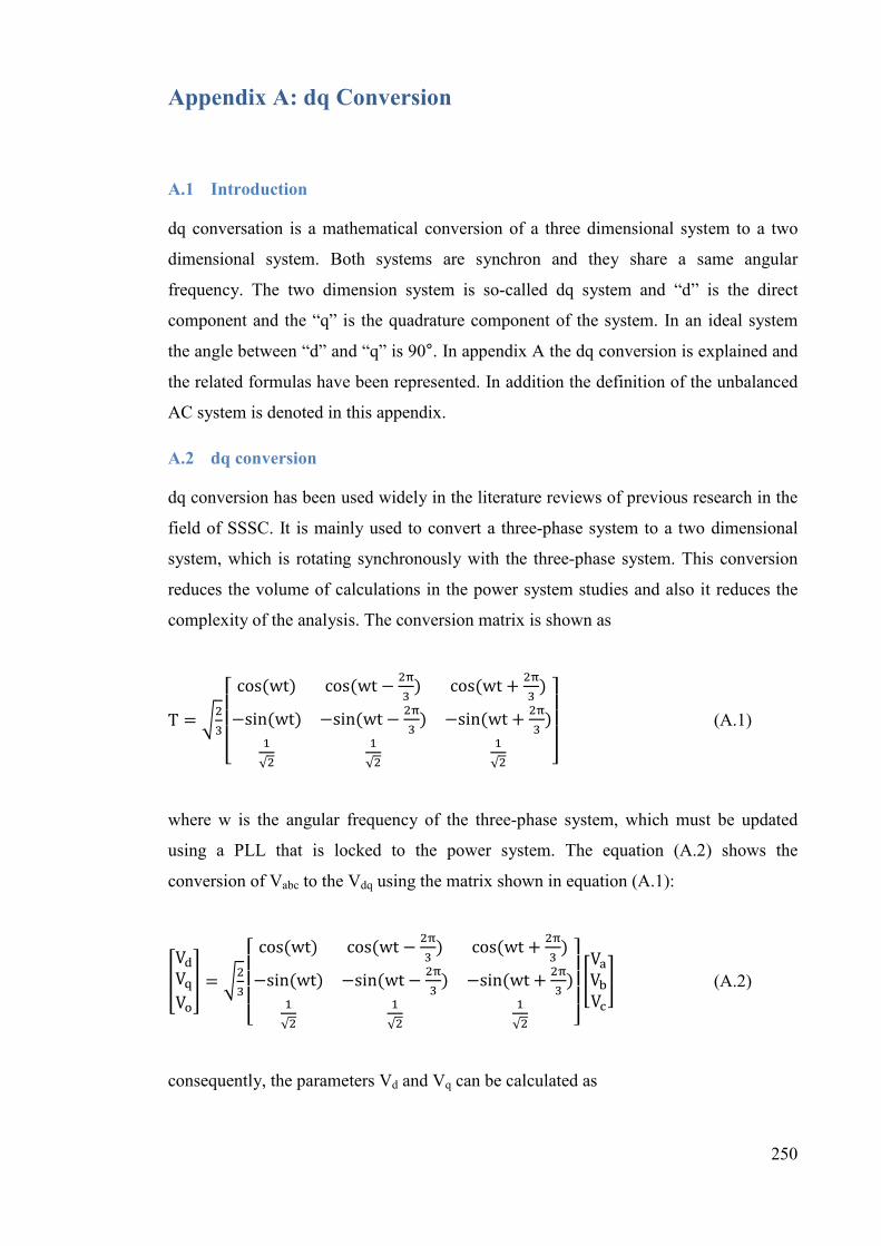
250
Appendix A: dq Conversion
A.1 Introduction
dq conversation is a mathematical conversion of a three dimensional system to a two
dimensional system. Both systems are synchron and they share a same angular
frequency. The two dimension system is so-called dq system and “d” is the direct
component and the “q” is the quadrature component of the system. In an ideal system
the angle between “d” and “q” is 90°. In appendix A the dq conversion is explained and
the related formulas have been represented. In addition the definition of the unbalanced
AC system is denoted in this appendix.
A.2 dq conversion
dq conversion has been used widely in the literature reviews of previous research in the
field of SSSC. It is mainly used to convert a three-phase system to a two dimensional
system, which is rotating synchronously with the three-phase system. This conversion
reduces the volume of calculations in the power system studies and also it reduces the
complexity of the analysis. The conversion matrix is shown as
T = %K cos(wt) cos(wt − %õK ) cos(wt + %õK )−sin(wt) −sin(wt − %õK ) −sin(wt + %õK )?√% ?√% ?√%
(A.1)
where w is the angular frequency of the three-phase system, which must be updated
using a PLL that is locked to the power system. The equation (A.2) shows the
conversion of Vabc to the Vdq using the matrix shown in equation (A.1):
¤V7V9V§ = %K cos(wt) cos(wt − %õK ) cos(wt + %õK )−sin(wt) −sin(wt − %õK ) −sin(wt + %õK )?√% ?√% ?√%
lVVéVo (A.2)
consequently, the parameters Vd and Vq can be calculated as
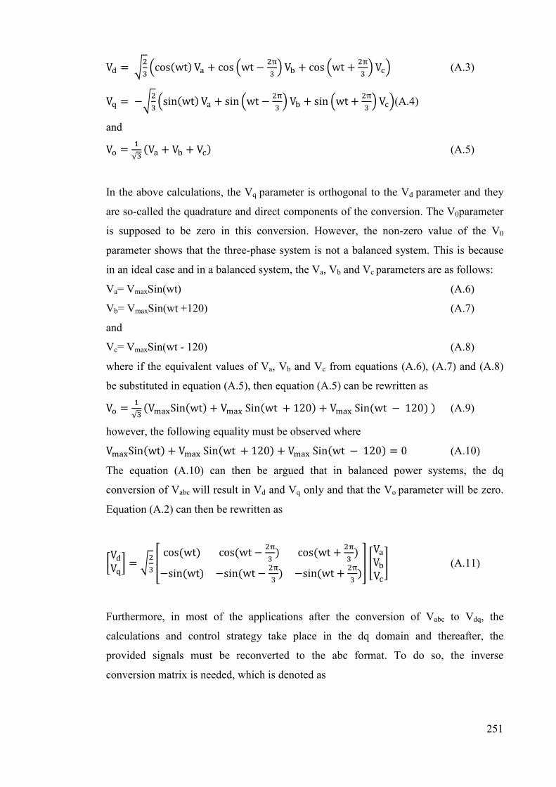
251
V7 =%K cos(wt) V + cos wt − %õK Vé + cos wt + %õK V (A.3)
V9 =−%K sin(wt) V + sin wt − %õK Vé + sin wt + %õK V(A.4) and
V = ?√K (V + Vé + V) (A.5)
In the above calculations, the Vq parameter is orthogonal to the Vd parameter and they
are so-called the quadrature and direct components of the conversion. The V0parameter
is supposed to be zero in this conversion. However, the non-zero value of the V0
parameter shows that the three-phase system is not a balanced system. This is because
in an ideal case and in a balanced system, the Va, Vb and Vc parameters are as follows:
Va= VmaxSin(wt) (A.6)
Vb= VmaxSin(wt +120) (A.7)
and
Vc= VmaxSin(wt - 120) (A.8)
where if the equivalent values of Va, Vb and Vc from equations (A.6), (A.7) and (A.8)
be substituted in equation (A.5), then equation (A.5) can be rewritten as
V = ?√K (VSin(wt) + VSin(wt + 120) + VSin(wt − 120)) (A.9)
however, the following equality must be observed where VSin(wt) + VSin(wt + 120) + VSin(wt − 120) = 0 (A.10)
The equation (A.10) can then be argued that in balanced power systems, the dq
conversion of Vabc will result in Vd and Vq only and that the Vo parameter will be zero.
Equation (A.2) can then be rewritten as
V7V9 = %K ¤ cos(wt) cos(wt − %õK ) cos(wt + %õK )−sin(wt) −sin(wt − %õK ) −sin(wt + %õK )§ lVVéVo (A.11)
Furthermore, in most of the applications after the conversion of Vabc to Vdq, the
calculations and control strategy take place in the dq domain and thereafter, the
provided signals must be reconverted to the abc format. To do so, the inverse
conversion matrix is needed, which is denoted as

252
T? = cos(wt) −sin(wt)cos(wt − %õK ) −sin(wt − %õK )cos(wt + %õK ) −sin(wt + %õK ) (A.12)
By applying the equation in (A.12), the Vabc parameter can be calculated from Vdq as
lVVéVo = cos(wt) −sin(wt)cos(wt − %õK ) −sin(wt − %õK )cos(wt + %õK ) −sin(wt + %õK )
V7V9 (A.13)
In all of the above calculations, it is assumed that the dq axes are synchronised with the
abc axes as shown in Fig.A.1. This means that the d-and a-axes are in the same direction
(aligned). However, this is not necessarily needed because there can be a phase
difference between them in some specific applications. For example, in SSSC or DSSC
applications, the introduced phase angleθ can be ±π/2 in order to create 90 degree phase
shift. The shifted dq axes are shown in red in Fig.A.1.
Fig.A 1: abc to dq
Considering the phase angle θ, equations (A.11) and (A.13) can be rewritten as
V7V9 = %K ¤ cos(wt ± θ) cos(wt − %õK ± θ) cos(wt + %õK ± θ)−sin(wt ± θ) −sin(wt − %õK ± θ) −sin(wt + %õK ± θ)§ lVVéVo (A.14)
and
lVVéVo = cos(wt ± θ) −sin(wt ± θ)cos(wt − %õK ± θ) −sin(wt − %õK ± θ)cos(wt + %õK ± θ) −sin(wt + %õK ± θ)
V7V9 (A.15)

253
In equations (A.14) and (A.15), the parameter θ represents the initial phase angle, which
will be useful when the dq axes needs to either lead or lag the abc axes.
A.3 Unbalanced Three Phase AC System
A typical unbalanced three-phase system is shown in Fig.A.2(a), which can be
compared with a three-phase balance system in Fig.A.2(b).
Fig.A 2: a) Unbalance three-phase system b) Balance three-phase system
In Fig.A.2 (a) the phase angles between the phasors in the unbalanced system are not
identical and their amplitudes are different. However, in a balanced system as seen in
Fig. A.2 (b), the angle is indistinguishable and the amplitudes are the same.
Furthermore, the unbalanced system disturbs the dq conversion and can lead to an
incorrect calculation. The unbalance of a three-phase system is defined by the
percentage of difference from the average voltage. This can be calculated as
PercentageofUnbalance = ?II∗ ∆!"± (A.16)
where Max ∆V is the maximum difference from the average voltage and VAve is the
average voltage.

254
Appendix B: Technical Characteristics of Components
B.1 Introduction
Technical characteristics of components and test rig are represented in appendix B. It
includes the components and electronics boards which are employed in the
implementation of the electronic and power electronics boards. The design process is
explained in chapter 4 then appendix B includes only the technical specifications and in
some cases the input and output layouts of the components and the related photo.
The test rig includes 220:50 transformer, DSSC device and all of the electronic boards
which are located inside an aluminium cage, as shown in Fig.B.1 a and b, with a
wooden base and net cover.
a) Aluminium cage of test rig

255
b) Inside test rig
Fig.0.1: Designed and implemented test rig
B.2 H-Bridge Converter
In the design of power electronics converter SK20GH123has been selected which is a H-
bridge compact module has been used. It can be easily secured to a top-mounting
copper heatsink with just one screw. It has well matched IGBT’s and diodes inside in
terms of rated voltage and current. Its IC-VCE curve for different VGE voltages is shown
in Fig. B.2. Based on the design the rated maximum voltage between collector and
emitter, VCE, in the off mode is 1.2 kV and the rated collector current, IC, is 23A at the
ambient temperature of 25°C. This current rating could go down to 15A at the
temperature of 80°C. The rated current for the freewheeling diode is 24A and 17A at
temperatures of 25°C and 80°C respectively [91].

256
Fig. B. 2: IC versus VCE curve
The SK20GH123 device, as shown in Fig.B.3, comes with 16 pins. These pins provide
access to different points of the H-bridge converter and IGBTs. Moreover, the
corresponding points of connection inside the SK20GH123 for pin numbers 1,2, 5, 7, 8,
9, 13 are shown in Fig. B.4 but the rest of pins including 3, 4, 6, 10, 11, 12, 14, 15 are
left unconnected, i.e. they are not applicable.
Fig.B.3: SK20GH123 device
Fig.B.4: The pin-configuration of SK20GH123 device

257
B.3 Buffer
SN74AHCT125 has been used in the gate driver board design. This device has 14 pins,
as shown in Fig.B.5, including four inputs, four outputs and four output-enabling (OE$$$$) inputs[93].
Fig.B.5: SN74AHCT125
The %&$$$$ input can disable or enable the output by being high or low respectively. If the output is enabled then it will follow the input. It means that the output will be equal to
the input. The relationship between input and output of each buffer is represented in
Table B.1.The logical diagram representing the functionality of the device along with
the related pin numbers is depicted in Fig.B.6.
Inputs Output %&$$$$ A Y
L H H
L L L
H X Z
Table B.1: Function table for each buffer
In this device, the high level output is equal to VCC and the minimum high level input is
2V while its maximum low level is 0.8 V. The input values between 0.8 V and 2 V will
not be recognised and the related output for these inputs will not be reliable but in the
gate driver the inputs will be 0V and 5V for the low level and high level input values
respectively. In order to disable one of the outputs, the related %&$$$$ is connected to VCC,
+5V, and irrespective of input the output will have no values. However, if %&$$$$ is connected to ground (zero volt) then the related output will be active and with

258
connecting the associated input to the 5 volts the output will be 5 volts. Also having 0
volt in the input will make output zero as well.
Fig. B. 6: Logic diagram of the SN74AHCT125
B.4 Gate Drive
The HCPL-3180 device includes an integrated GaAsP LED which is providing optical
coupling, as shown in Fig.B.7, between input and output. This device comes with 8 pins
where pin numbers 1 and 2 are not connected; pin number 2 and 3 are connected to
anode and cathode respectively. Pin number 8 and 5 are used for VCC and VEE
connection. Pin numbers 7 and 6 are connected to the VO jointly [109].
Fig. B. 7: Functional diagram of HCPL-3180
With reference to the data sheet [68] there must actually be a minimum positive voltage
of 1.2V across the anode-cathode in order to trigger the GaAsPLED. The recommended
voltage in data sheet is 1.5 V therefore, the forward voltage of diode is considered as
1.5V in the design. On the other hand the output voltage of the buffer is 5 V and the
voltage across the resistor will be 3.5V and referring to the data sheet [109] the
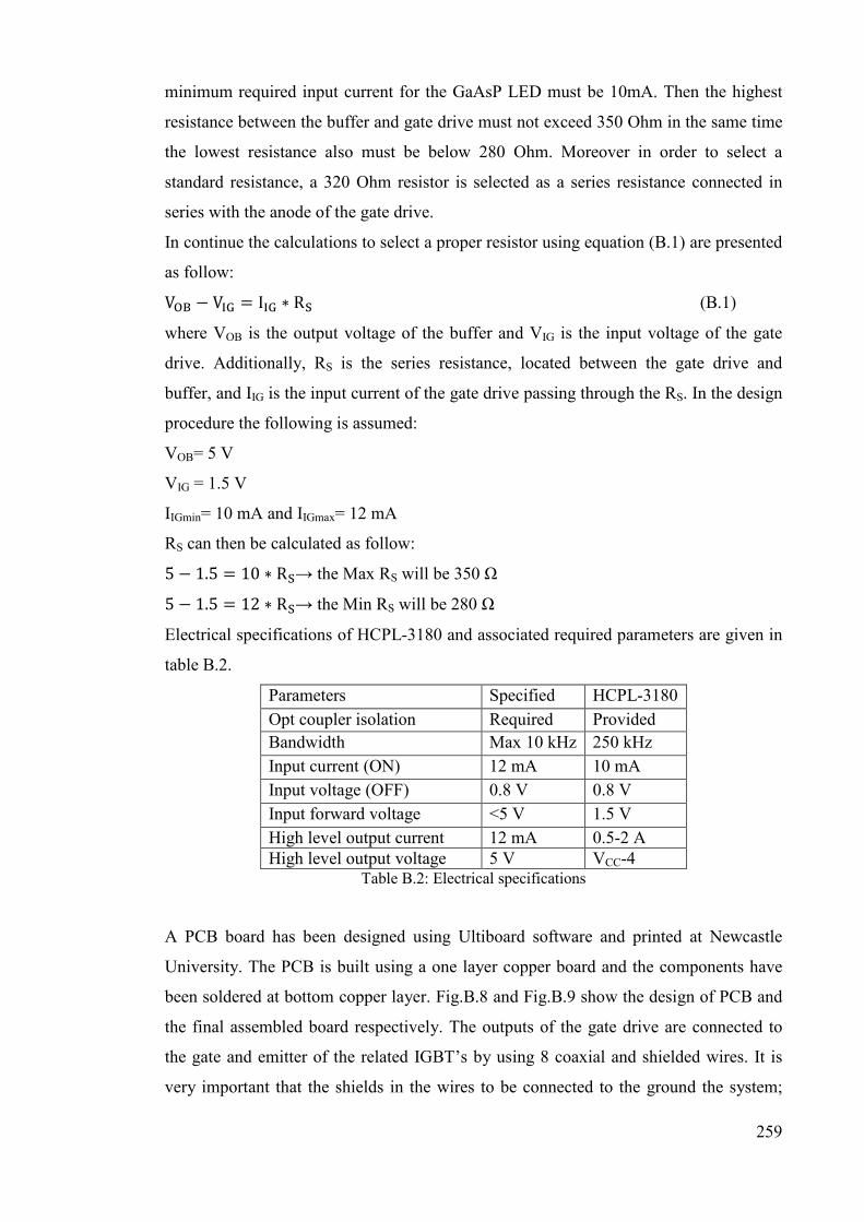
259
minimum required input current for the GaAsP LED must be 10mA. Then the highest
resistance between the buffer and gate drive must not exceed 350 Ohm in the same time
the lowest resistance also must be below 280 Ohm. Moreover in order to select a
standard resistance, a 320 Ohm resistor is selected as a series resistance connected in
series with the anode of the gate drive.
In continue the calculations to select a proper resistor using equation (B.1) are presented
as follow: Våü − VÖ = IÖ ∗ R (B.1)
where VOB is the output voltage of the buffer and VIG is the input voltage of the gate
drive. Additionally, RS is the series resistance, located between the gate drive and
buffer, and IIG is the input current of the gate drive passing through the RS. In the design
procedure the following is assumed:
VOB= 5 V
VIG = 1.5 V
IIGmin= 10 mA and IIGmax= 12 mA
RS can then be calculated as follow: 5 − 1.5 = 10 ∗ R→ the Max RS will be 350 Ω 5 − 1.5 = 12 ∗ R→ the Min RS will be 280 Ω
Electrical specifications of HCPL-3180 and associated required parameters are given in
table B.2.
Parameters Specified HCPL-3180
Opt coupler isolation Required Provided
Bandwidth Max 10 kHz 250 kHz
Input current (ON) 12 mA 10 mA
Input voltage (OFF) 0.8 V 0.8 V
Input forward voltage <5 V 1.5 V
High level output current 12 mA 0.5-2 A
High level output voltage 5 V VCC-4 Table B.2: Electrical specifications
A PCB board has been designed using Ultiboard software and printed at Newcastle
University. The PCB is built using a one layer copper board and the components have
been soldered at bottom copper layer. Fig.B.8 and Fig.B.9 show the design of PCB and
the final assembled board respectively. The outputs of the gate drive are connected to
the gate and emitter of the related IGBT’s by using 8 coaxial and shielded wires. It is
very important that the shields in the wires to be connected to the ground the system;

260
otherwise noise can be induced through the wire and it can generate unwanted
switching. Even the length of the wire must be as short as possible in order to avoid any
possible induced noises.
Fig.0.8: Design of PCB Gate Drive Board
Fig.0.9: Implemented Gate Drive Board
B.5 Isolated power supply
Isolated power supply provides isolation between electronic signals and power circuit.
This device, NMF0515S, is shown in Fig.B.10 which is a DC/DC converter [94].The
device comes with 5 pins where pin numbers 1 and 2 are connected to the supply
voltage of 5 V.Pin numbers 3 and 5 provide the output voltage of 15V. Its rated output

261
power is 1 Watt and requires no heat sink. It also can provide output current of 67 mA
[94].
Fig. B. 10: NMF0515S DC/DC converter
Its output power capacity may reduce by an increase in the operating temperature. The
reduction in output power starts from 70° and up to this point it can deliver 100% of the
rated power. After this point, the output reduces linearly with an increase in the
temperature. For example at 100° the output power is halved. Moreover when the
temperature reaches 125°, the output converges to zero. The safe operation zone is
shown in Fig. B.11 [94].
Fig. B. 11: Safe operation zone and out power of MNF0515S at different ambient temperatures
In general, switching ON and OFF of IGBT consumes some energy which must be
provided by the gate drive and gate drive power supply. The amount of required energy
depends on the gate charge characteristics of the selected IGBT and the switching
frequency. The average current which must be supplied is given as follow: IEFG = QÖ ∗ få (B.2)
where fO is the operation frequency and QG is the total gate charge. The operating
frequency in this experimental study is about 1 KHz and the total gate charge can be
found from gate charge characteristics curve which comes with data sheet of the IGBT.
For SK20GH123 IGBT the gate charge characteristics is depicted in Fig.B.12 and can

262
be easily observed that for the IGBT, in order to reach its nominal current, it requires 90
nC energy. Therefore the average current will be:
IAve = 90 * 1000 = 0.9 mA
and the required power which must be provided is calculated as follow: PG9 = IEFG ∗ ΔV (B.3)
wherePreq is the required power to turn on the IGBT so that the current through
collector-emitter to reach its nominal value. Also ∆V is the range of change of the gate-
emitter voltage from OFF to ON status or vice-versa. The gate-emitter voltage changes
from -15 to 15 so the ∆V will be 30 volts. Therefore Preq is calculated using (B.3) as
Preq = 0.9 * 30 = 27mW
Referring to the data sheet of the gate drive isolated power supply [94], its output power
is 1W, enough to supply the gate drive to turn ON and turn OFF the IGBT. In addition,
referring to data sheet of the gate drive, its output power is 600mW which is enough to
provide Preq as calculated above.
Furthermore, it must be noted that the experimental studies are conducted in order to
prove the validity of the proposed control idea which is discussed earlier in chapter 4.
However in these studies the collector-emitter current in ON status of the IGBT due to
the restriction on the equipment and the available facilities in the UG lab is designed not
to exceed 15 A. But yet full Preq is required in order to force IGBT to fully conduct the
current. For this reason, although the collector-emitter current will rarely reach 15A, but
the gate-emitter voltage is designed to be 15V and the Preq will be 27mW.
Fig.B.12: Gate charge characteristics of SK20GH123

263
Despite a small amount of power is required to turn on and turn off the IGBT, a
considerable high peak current is required in order to provide an efficient switching.
This is because having sufficient current, the required energy will be supplied quickly
and the switching will be performed faster. To do so, the gate current must be increased
up to the specified permissible value. This value is determined mainly by the output
current of the gate drive which is 2.5 A for the HCPL-3180.
B.6 Voltage Transducer (VT)
Voltage transducer is a key component in the voltage measurement board. The LV 25-P
VT is shown in Fig. B.13. The measurement of voltage can be achieved by passing a
current through the transducer which is proportional to the measured voltage and can be
controlled by an external resistor. In the calculation of the resistance it must be noted
that the optimum accuracy of the device can be achieved if the primary input current in
the measuring of the nominal voltage become 10 mA [95].
Fig. B.1: LV 25-P the selected voltage transducer
In addition the accuracy of VT depends on the value of input current and refer to the
data sheet of the LV 25-P [95] its accuracy is 0.8% for IPN=10 mA and 1.5% for
IPN=5mA. Furthermore, the turn ratio of the transducer is 2500:1000 and with nominal
current at the input the nominal output current will be 25 mA. In order to convert the
output current to the voltage and make it useable by the electronic circuit a resistor, RM,
needs to be connected between output pin and ground of the electronic board in the
measurement board. The connections of the VT and related pins are shown in Fig.B.14.
In this device +HT and –HT are positive and negative polarity of connections of the
input voltage. +VC and –VC are the supply pins. The output is shown by M and it must
be connected directly to the RM resistor.

264
Fig. B.2: Connections of VT
As a part of the hardware design and implementation, a PCB board which is shown in
Fig.B.15 is designed using Ultiboard software. The designed PCB is printed in the
Newcastle University and afterward the other devices are populated. After
implementation, the board itself was tested and validated using fixed AC and DC
voltage sources. The final implemented voltage measurement board is shown in
Fig.B.16.
Fig.B.15: PCB designed voltage measurement

265
Fig.B.16: Implemented voltage measurement board
B.7 Op-Amp
LMC660CMOp-amp chip is used in the voltage and current measurement boards. It is
used to boost up the main signals (i.e. voltage or current) and eliminate the unwanted
signals. It includes four Op-amps and its connection diagram is shown in Fig.B.17. As
long as its electrical features concern it must be noted that it has rail to rail output swing
therefore, the output voltage can dynamically vary between VSS and VEE [96].
Fig. B.3: Connection diagram of the LMC660CM

266
B.8 Current Transducer
Current transducer LTS 25-NP shown in Fig.B.18 is employed in the current
measurement board. Its accuracy is ±0.2 % at nominal input current and temperature of
25°C [97].
Fig.B. 4: LTS 25-NP Current Transducer
The I-V characteristic of the CT presented in Fig.B.19 shows that for input currents
above the absolute value of IPmax the output voltage remains unchanged, i.e. gets
saturated. The output voltage for input currents above IPmax will retain in the fixed value
of 4.5 volts and for currents less than -IPmax will remain in 0.5 volts. IPN (nominal input
current) for this current transducer is 25 A then with the nominal input current the
output voltage will be 3.125 V. It can be concluded that the permissible output voltage
margin to measure the currents between 0 up to 25 A is 0.625 V.
Fig.B.5: I-V characteristic of LTS 25-NP Current Transducer
However if the CT is supposed to be used to measure lower currents then different
configurations of the input can be used in order to achieve the accuracy of 0.2 %. To do

267
so, three different configuration of CT can be used as depicted in Table B.3. For
example, for input currents about 25 A it is recommended that pin numbers 1, 2, 3 to be
connected together and pins 4, 5, 6 also to be tied together as well then the turn ratio of
1 will be selected in the transducer.
Number of Primary Turns
Primary Nominal Current rms IPN [A]
Nominal Output Voltage VOut [V]
Recommended Connections
1 ±25 2.5±0.625
2 ±12 2.5±0.600
3 ±8 2.5±0.600
Table B.3: Different configuration of CT with different turn ratio
The connection of LTS 25-NP is shown in Fig. B.20. It shows that the CT can be
supplied by 5 V DC and the ground is shared between supply voltage and output
voltage. In this diagram, the input current is shown by ±IP which can be shared between
input pins 1, 2, 3 and output pins 4, 5, 6. The turn ratio of CT can be changed by
choosing one of the connections in Table B.3.It is noted that if the direction of input
current is from pins 1, 2, 3 to 4, 5, 6 the polarity of the output voltage will be positive. If
the direction of input current changes then the polarity of output voltage will be
negative. Despite of this the output voltage is still positive (minimum 0.5 volts) because
there is 2.5V offset at the output. However the change of direction must be considered
in the calculations.
Fig. B.20: Connection in LTS 25-NP Current Transducer

268
A PCB is designed for the current measurement board using Multisim and Ultiboard
software. The designed PCB is printed at Newcastle University and it layout is shown in
Fig.B.21.
Fig.B.21: layout of designed and printed PCB for current measurement board
After printing the PCB, other components including p-amps, CT, resistors etc... have
been soldered in the UG lab as a part of the implementation process. The final
completed current measurement board is shown in Fig.B.22.

269
Fig.B.22: The current measurement board

270
Appendix C: Microcontroller
C.1 Introduction
A microcontroller is needed to run the control algorithm. The algorithm is being
executed by CPU which is the main part of a microcontroller. However a CPU sends
commands and receives information by importing and exporting of data. Then a
microcontroller needs to provide a proper input and output (I/O) ports in order to be
able to run an algorithm and control a plant. The received signals are in an analogue
format and their configuration needs to be converted to digital. This is achieved with an
analogue to digital (A/D) converter within the microcontroller. The digital data is
handled using data memory access (DMA) in the microcontroller and this can avoid
involvement of CPU in data management. In addition the control algorithm of the
DSSC includes a PWM generator. This functionality either can be provided by the
microcontroller itself as an embedded function or it can be written in a code and
executed by the CPU.
In appendix C the employed microcontroller, dsPIC33FJ256MC710, in the
implementation of test rig is explained. The microcontroller comes with embedded
board and it includes its own PWM generator, A/D, I/O ports and DMA.
C.2 Microcontroller
The selected board is shown in Fig.C.1 with description of different parts. The
microcontroller (dsPIC) itself needs to be supplied by 3.3 V, which comes from a robust
on-board power supply. This power supply is well regulated for 9V-36V input voltage
range. Other different voltage levels for the different parts of the board are provided
internally. Even the polarity of the input voltage of the board is not important and a
voltage between the permitted margins can be used in the input. Robustness of the
embedded board in terms of using wide range of voltages, no matter what polarity they
have, makes the embedded board flexible and easy to use. In the designed test rig, the
embedded dsPIC board is supplied with + 9V via a DC power distribution feeder which
is built to supply the electronic boards within the test rig. Additionally, the dsPIC can be
supplied externally via available connectors and the reference voltage for the ADC can
be altered and provided externally [110].

271
Fig. C. 1: dsPIC33FJ256MC710 within an embedded board
It can be observed from Fig.C.1 that the board comes with six different LEDs. They
facilitate monitoring different status of operation of the board. Different operation mode
of the board is indicated by the related LEDs which they come in different colour in
different operation mode. More details of each LED and related colour can be found in
table C.1 [110].

272
LED Colour Function
DL1 Green Input power supply
DL2 Green Internal +5V power line activity
DL3 Green Internal +5V power line activity
DL4 Yellow dsPIC (R) DSC controlled led (e.g., debugging purposes)
DL5 Yellow Internal PIC18 controlled led
DL6 Red USB cable connection monitor
Table C.1: Colours of LEDs indicating different functionality of the board
As soon as the power supply is connected, the DL1 becomes green indicating input
power supply is on.
The dsPIC’s pins are available at the connectors which are shown in the Fig.C.1 [92].
The connectors assign easy access to all the pins in the microcontroller. The signals
coming from the measurement boards, as well as the signals going to the gate drive
board, are connected to the dsPIC via these connectors. The pin configuration of the
dsPIC33FJ256MC710 is shown in the Fig.C.2 which is a Thin Quad Flat Pack (TQFP)
100 pin chip. Pin numbers 93 (PWM1L), 94 (PWM1H), 98 (PWM2L) and 99
(PWM2H) are used as PWM outputs. Pin numbers 25 (AN0), 24 (AN1) and 23 (AN2)
are used as analogue inputs for two voltage signals and one current signal coming from
the measurement boards. All pins are accessible by sockets provided in the board. This
facilitates direct access to the dsPIC.

273
Fig.C.2: Pin diagram of dsPIC33FJ256MC710
It operates like an interface and must be used along with MPLAB software installed in
the PC. It gives the opportunity for the programmer to see the status of the registers in
the breakpoint [74]. The program written in C code is then compiled using MPLAB
software and uploaded to the controller via MPLAB ICD 2 (shown in Fig. C.3). Once
running the program in the microcontroller, the status of the variable and registers can
be downloaded to the PC again using the MPLAB ICD 2. This communication even

274
allows amending the value of registers which can be very useful in debugging the
program [99].
Fig. C. 3: MPLAB ICD 2
C.3 Direct Memory Access (DMA)
Direct Memory Access (DMA) is used to manage data between the CPU and other
peripherals in the dsPIC. This helps the CPU not to be involved in transferring data
between the registers. The peripherals which are involved with DMA in this project are
[93]:
ADC
Input Capture
Output compare
Each DMA must be configured properly to carry out specific functions. There are six
different registers in the DMA controller which need to be set to certain values. For
example, DMAxCON configures channel x to carry out a certain mode of operation.
Also Enabling or Disabling the channel is done by this register. As another example,
DMAxCNT deals with the numbers of requests from DMA which must be set in DMA
controller.
In this project, DMA is set for peripheral indirect mode and continuous, not Ping-Pong
mode. The related code is as follow:
void initDma0(void)
DMA0CON = 0x0000; // no increment
DMA0CONbits.AMODE = 0; // Config DMA for Peripheral indirectmode
DMA0CONbits.MODE = 0;// Config DMA for Continuous no Ping-Pong mode
DMA0CNT=3; // 4 DMA request
DMA0REQ = 13; // 0001101 = ADC1 – ADC1 Convert

275
DMA0PAD=(int)&ADC1BUF0;
DMA0STA = __builtin_dmaoffset(DMA0_buffer);
DMA0CONbits.CHEN=1; // Enable DMA
IFS0bits.DMA0IF = 0; //Clear the DMA interrupt flag bit
IEC0bits.DMA0IE = 1; //Set the DMA interrupt enable bit
DMA0CONbits.CHEN=1; // Enable DMA
C.4 PWM Generator
ThedsPIC33FJ256MC710 has four PWM generators. Each of them can be configured
independently. In this project two of them have been employed in order to trigger four
IGBT’s in the H-bridge converter. Each PWM generator has two outputs, high and low,
which can be in complimentary or independent mode. For example, in the
complimentary mode if the high value output has logic “1” then the low value output
definitely is “0”. However, in the independent mode the low value output is not
necessarily “0” and can be “0” later on.
The PWM generator can be configured to insert dead time in the transition from low to
high or high to low status. This is a very useful capability of the PWM generator when
generating two outputs from one single PWM signal in order to trigger two IGBTs in
one leg. If two IGBTs in one leg of the converter conduct at the same time then it will
create a short circuit, thus will discharge the DC capacitor. By introducing dead time
between the switching times of the IGBTs there will be no short circuit in the related
phase.
Output of PWM can operate in different modes as follow [112]:
• Single Event PWM Operation
• Edge Aligned PWM Mode
• Centre Aligned PWM Mode
• Complimentary PWM Output Mode
The Centre Aliened PWM mode has been used in this project then only this mode is
explained here and further information regarding the other modes of operations can be
found in [96].The centre aligned PWM mode, as shown in Fig.C.4,usesPxTMR, PxDC
and PTPER parameters to generate PWM pulses. For example in half period when the
PxTMR reaches to the PxDC value the related PWMxH output becomes zero (low
level). The output value is zero till the second half period when the PxTMR again

276
becomes equal to the PxDC and the output becomes “1”. The change of value of output
happens each time PxTMR become equal to the PxDC.
However this change depends on the mode of PxTMR. For example, when PxTMR is in
up counting mode then the output value will change from “1” to “0”. There will be other
way around when the PxTMR is in down counting mode. The mode of PxTMR changes
when the value of PxTMR reaches the PxTPER. This event happens twice per period as
it is explained in continue. Initially, the PxTMR value is zero then it starts to count up
until it reaches the PxTPER value. This time interval is equal to half period and at this
point PxTMR starts to count down. After another half period the PxTMR reaches to
zero which is the time again to switch to up counting mode.
Fig. C. 4: Centre aligned PWM mode
In dsPIC33FJ256MC710 each PWM generator can produce two PWM pulses with
different duty cycles but with the same frequency. This can be obtained by using
different PxDC values; each of them can generate different pulses in the corresponding
output. The value of PxDC is updated by the reference signal at each clock. With new
value of PxDC then the generated pulse will be different and of course updated. This
process makes the producing of the demanded waveform (in our project a sinusoidal
voltage which is orthogonal to the line current) become possible by the converter. The
value of PxTPER determines the frequency of carrier signal in the PWM generation.
This is so called chopping frequency in the PWM and it can be increased or decreased
by decreasing or increasing the PxTPER, respectively.

277
The PWM generator can be configured to operate in different mode with different
functionalities. Such a configuration is represented in the following code. For example,
the PWM outputs can be selected to operate in pair or single mode. Having the pair
mode selected, the pin pairs can be either in the Independent output mode or in
Complementary output mode. In the independent mode each of pin pairs can hold either
values of “0” or “1”. It means that both in the same time could have value of “1” or “0”.
In complementary mode if one of them is high the other is necessarily low.
In the DSSC prototype project the complementary mode is selected. This is because in
H-bridge converter there are two series-connected IGBTs in each leg of converter and if
they are triggered at the same time then there will be a short circuit in the DC bus. In
order to avoid such a failure they must be protected against being “ON” at the same
time.
After selection of the mode of operation for the outputs, the outputs themselves must be
activated. This is activated by Enable/Disable bit for the corresponding output in the
configuration register of the related PWM generator. For example, in order to enable the
“HIGH” output of the PWM1 the “PWM1CON1bits.PEN1H”, as it is represented in the
following code, must be set to “1”.
As explained earlier the PxTPER is employed in PWM generator to achieve the desired
chopping frequency. Normally this frequency remains unchanged during the operation.
The PxTPER can be calculated as
PxTPER = )*)Þ+,?% (C.1)
where PxTPER is related to half of the period of the carrier signal, FCY is the
instruction clock of the dsPIC. This FCY determines the speed of operation of the
device. With dsPIC33FJ256MC710 operation frequency of 40 MHz can be achieved.
FPWM is the chopping frequency of the carrier signal. For example, if using FCY of 20
MHz in order to achieve PWM frequency of 20 kHz, PxYPER can be calculated as
PxTPER = ~ý,-.~ýà-.?% = ÒÒÒ% = 499.5 ≅ 499 (C.2)
The PxDC, the duty cycle of the pulses, are changing all the times during the operation.
Source of changes is the reference signal itself. For this reason, there is a facility in the
PWM generator which provides opportunity to update the PxDC immediately after any
change within the reference signal. Also, the update can be taken place at the end of
each clock. In the prototype implementation, the update is set to be taken into account at
the end of each clock in order to avoid disturbances.

278
voidinit_PWM()
P1TCONbits.PTCKPS = 0b00;
P1TCONbits.PTOPS = 0b0000; //<3:0>: PWM Time Base Output Postscale Select bits
P1TCONbits.PTMOD = 0b11; //<1:0>: PWM Time Base Mode Select bits ---11 =
PWM time base operates in a Continuous Up/Down mode with interrupts for double
PWM updates
PWM1CON1bits.PMOD1 = 0;
PWM1CON1bits.PMOD2 = 0;
PWM1CON1bits.PMOD3 = 0; // PWM I/O Pair Mode bits
FPOR1bits.HPOL=0 ;//1 = PWM I/O pin pair is in the Independent Output mode
//0 = PWM I/O pin pair is in the Complementary Output mode
PWM1CON1bits.PEN1H =1;
PWM1CON1bits.PEN1L = 1;
PWM1CON1bits.PEN2H = 1;
PWM1CON1bits.PEN3H = 1;
PWM1CON1bits.PEN2L = 1; // PEN4H=1 PWMxH4 I/O Enable bits(1,2)
PWM1CON1bits.PEN3L = 1;
PWM1CON2bits.IUE = 0; //IUE=1 Immediate Update Enable bit
PWM2CON2bits.IUE = 0;
PTPER = 6500; /* PTPER = ((1 / 400kHz) / 1.04ns) = 2404, where 400kHz
//PTPER = 1000; // is the desired switching frequency and 1.04ns is PWM resolution. */
/*~~~~~~~~~~~~~~~~~PWM1Configuration ~~~~~~~~~~~~~~~~~~~~~*/
PDC1 = 640; /* Initial Duty cycle */
/* Clock period for Dead Time Unit A is TcY */
/* Clock period for Dead Time Unit B is TcY */
P1DTCON1bits.DTAPS = 0b00;
P1DTCON1bits.DTBPS = 0b00;
/* Dead time value for Dead Time Unit A */
/* Dead time value for Dead Time Unit B */
P1DTCON1bits.DTA = 8;
P1DTCON1bits.DTB = 5;
/* Dead Time Unit selection for PWM signals */
/* Dead Time Unit A selected for PWM active transitions */

279
P1DTCON2bits.DTS3A = 0;
P1DTCON2bits.DTS2A = 0;
P1DTCON2bits.DTS1A = 0;
P1DTCON2bits.DTS3I = 1;
P1DTCON2bits.DTS2I = 1;
P1DTCON2bits.DTS1I = 1;
P1TCONbits.PTEN = 1; // PWM Time Base Timer Enable bit Enabling PWM Pulse
Generation
//1 = PWM time base is on
//0 = PWM time base is off
C.5 Analogue to Digital Converter (ADC)
Analogue signals come from the measurement boards need to be converted to the digital
format and this is achieved in microcontroller through means of an ADC. In the
laboratory prototype DSSC test rig, the employed microcontroller,
dsPIC33FJ256MC710, includes an integrated ADC. The block diagram of the ADC
module is shown in Fig.C.5, where it comes with 32 analogue inputs connecting to pins
AN0 AN1...AN31.These inputs can be selected by using the control bits to be connected
to a sample and hold devices. This will provide an opportunity to control the incoming
signals and decide to connect the desired signal within a proper timing to the ADC. It
means that all of the inputs eventually can be connected to the ADC but this can happen
only if the related control bit becomes “1”[94].
One of the key features of the ADC module is that it can take an external reference
signal instead of an internally provided one. This feature can be used to manipulate the
conversion resolution. However in the DSSC prototype implementation the internal
reference signal has been employed in order to avoid complexity. Also the ADC module
supports DMA which allows the data to be stored in the memory without using CPU.
This attribute of ADC saves time and consequently speeds up the operation of device.
The ADC module, like other parts of the dsPIC33FJ256MC710, has its own
configuration registers. These registers allow selecting different configuration of the
module. For example, the analogue input channel s can be selected and configured using
these registers. Even the “ON” and “OFF” mode of ADC can be controlled by
allocating “1” or “0” to the associated register. In the DSSC prototype inputs AN1, AN2

280
and AN3 are allocated as analogue inputs. These three inputs receive analogue signals
from current and two voltage measurements.
Fig.C.5: The block diagram of the ADC module

281
C.6 I/O Ports
I/O ports are used to send or receive data in order to monitor and control the other
devices. In the dsPIC33FJ256MC710 all the pins can be employed as I/O ports except
pins for supply (such as VDD or VSS) and the pins used for clock and oscillator
(OSC1/CLKL). A dedicated port model is shown in Fig.C.6 where each port can be
configured to be “Input” or “Output” [92].
Fig.C.6: A typical block diagram of I/O port
Each I/O port needs four registers namely, TRIS, PORT, LAT and ODC in order to be
set to operate in desired mode. For example, the TRIS register defines the flow direction
of data by enabling the I/O port to be “Input” or “Output”. When the TRIS register (for
the corresponded I/O port) is set to “0” it means that the port is an “Output” while “1”
in the TRIS register shows that the corresponded port is an “Input”. “PORT” register
allows reading or writing of the corresponding I/O pin. To do so, some instructions like
“BSET” or “BCLR” are needed to be used. For instants, the example code for “BSET”
can be as follow:
BSET PORTA, #0 ; Set pin 0 on Port A to ‘ 1’

282
BSET PORTA, #1 ; Set pin 1 on Port A to ‘ 1’
In the above code, the “BSET” instruction sets value of “1” to the port “A”. However,
reading from and writing into the port can be problematic if the read and write follows
each other (so-called “Read-Modify- Write” mode). The problem can occur when these
instructions want to be executed one after each other while the voltage in the
corresponding pin has not reached to the target level. In occurrence of this problem,
wrong data will be presented in the I/O pin. In order to avoid the fault the “LAT”
register must be employed. In the “Read-Modify-Write” operation the data can be red
from the port latch and is written in the I/O port pin. The following code shows the
writing on the I/O port using LAT register.
BSET LATA, #0 ; Set pin 0 on Port A to ‘ 1’
BSET LATA, #1 ; Set pin 1 on Port A to ‘ 1’
There is no difference between LAT and PORT register when they are used to write to
the I/O port. However, using these two registers to read from I/O port can result in
different values. For instance, LAT reads the previous value which was held in the port
but PORT reads values which are currently on the port.

283
Appendix D: Application of DSSC in Distribution Networks;
Feasibility Study
D.1 Introduction
Feasibility of DSSC application in the existing 11kV distribution networks, in terms of
their mechanical withstand capability, has been studied. The study includes overhead
line design considerations and evaluation of the strength of poles. The study identifies
important mechanical factors which must be considered in application of DSSC in the
electrical networks. The study focuses mainly on the existing networks and employed
equipments within their design. For example, the poles used in the construction of low
voltage overhead lines are not as strong as transmission line towers and they can be
made of different type of wood or metal. The overhead line wires can also be made of a
wide range of conductors and materials. In addition, the effect of environmental
conditions such as wind and the consequence oscillations has been studied.
D.2 Overhead Line Design Consideration
The mechanical construction of an overhead line, and its maintenance, requires a lot of
attention in the design process of the line. Generally the most likely element to fail in an
overhead line is the conductor and this can happen because of high winds or
overloading of the line due to ice. For example, most of the reported overhead line
failures in 11kV distribution circuits are related to line breakages [113]. Long spans
increase the possibility of conductor clashing and may cause some damage at the
contact points. This will weaken the strength of the wires and increase the likelihood of
a break down in windy or bad weather conditions. For these reasons, care must be taken
to ensure that the extra weight presented by the suspension of DSSC devises from the
line conductors is fully taken into account when considering the application of DSSC.
D.2.1 Restricted vibration
Vibrations in an overhead distribution line can be divided into two categories. The first
is an oscillation with large amplitude and low frequency referred to as Galloping and is
generated by winds with speed of 5-10 miles/s. This type of vibration usually occurs in
locations with long spans, for example where lines cross rivers or highways. The second

284
type is referred to as Aeolian vibrations and is a vertical vibration with low amplitude
and normally with the frequency of about the natural frequency of the line.
With regard to the Galloping, the suspension of DSSC from existing lines acts like
added inertia and will initially contribute toward damping of any small amplitude weak
oscillations in the line. However, as the large amplitude oscillation starts, for example
as a result of strong wind, the extra weight of the DSSC device will boost the oscillation
and may lead to a clash between the lines.
Fig.D.1: Decomposition of mechanical forces
The decomposition of mechanical forces in a DSSC compensated line is shown in
Fig.D.1. In the figure, F is a mechanical force pointing toward the ground due to the
mass of the line and the DSSC device. Under normal conditions, i.e. no oscillation, F2 is
zero and F1 is equal to F. However, as the line moves to the side as a result of Galloping
F will be decomposed into the two orthogonal forces F1 and F2 with F2trying to force a
return back to the pervious conductor location. Thus, and in accordance with Newton
laws of motion, it may be concluded that the extra mass of the DSSC device will help
stop the initialisation of Galloping. However if as result of strong winds Galloping is
initiated, the extra mass means that it may become more difficult to stop. Therefore
where there is a likelihood of Galloping, in areas like river or highways crossings (in
locations with long span), the installation of DSSC is not recommended in those
sections of the line. Because of the distributed nature of the compensation, however,
this will have a minimal effect on the performance of the line as a whole.
Aeolian vibration on the other hand is not directly related to the weight of the wire and
will not be significantly affected by the presence of DSSC devices in the power lines.
This kind of vibration is caused by continuous wind and the margin for this movement
is similar to the wire dimensions.

285
D.2.2 Conductor tension
Conductor tension is generated by the line mechanical load which is a combination of
wind force and weight of the conductor. The former is mainly horizontal and is referred
to as the Maximum Conductor Pressure (MCP), while the latter is a vertical load and is
referred to as the Maximum Conductor Weight (MCW). The maximum permissible
tension of the conductor is the tension which the conductor can stand at a temperature of
−5.6°C, considering the effects of all loads including wind pressure and weight. The
maximum tension of the conductor must of course be within certain safety limits. The
suspension of DSSC modules, however, means that there is a possibility of the resultant
tension exceeding the existing safety margins as a result of the extra weight of the
modules.
Fig.D.2: Interaction between the forces in a compensated distribution line
Fig. D.2 shows the forces generated by the mass of the line, the mass of the DSSC
module and the forces generated in the line to counter the resultant force. In the figure,
F2 is generated by the mass of the DSSC module and is equal to mDg, where mD is the
mass of the DSSC device and g is the gravitational acceleration. F1 represents the force
generated by the mass of the line and is equal to mlg where ml is the mass of the line
section between two poles. F is the sum of the two forces F1 and F2. In order to counter
the effect of F, the line generates the force FH, which may be decomposed into two
orthogonal components, −F and Ft, as shown. The force −F has exactly the same
magnitude as F but acts in the opposite direction while Ft is the force which creates
tension in the wire. The line tension will therefore increase with any increase in F. For
this reason the effects of adding the external weigh represented by the DSSC modules
must be carefully studied.
The tensions withstand capability of a power overhead line varies from line to line
depending on the dimensions, materials and geometry of the wires. The characteristics

286
of Aluminium alloy, as a commonly used conductor for 11kV overhead lines, is selected
for investigation in this study. A conductor with a cross sectional area of 180.7 mm2 has
a mass of approximately 497 kg per km, with a calculated breaking load of 50.65 kN
[60]. Assuming that each DSSC module has a mass of approximately 50 kg (typical
weight of DSSC as mentioned in [50]) and considering the mass of 0.4 km section of
the line (the maximum span length for medium class poles) then the wire must be able
to withstand (0.4*497+50) kg. The force produced by such a mass is around 2.4kN and
is less than the calculated breaking load for the wire. So, in this case suspension of
DSSC modules from the wire may not be problematic in terms of the calculated
breaking load. Using another example of a standard aluminium alloy stranded conductor
(with a cross sectional area of 30.10 mm2 and an approximate mass of 82 kg/km) the
calculated breaking load is 8.44 kN. By adding the weight of the DSSC device, the total
load will be 82.8 kg which produces a force of 0.8 kN, still less than the breaking load
of the conductor. However, as the cross sectional area of the wire becomes smaller the
ratio of breaking load to the resultant load becomes smaller and care must be exercised
when considering the implications of DSSC.
Cross
sectional area
Mass per
kilometer
Calculated
breaking load
Total load
with DSSC Ratio of breaking load over the total load
30.10 mm2 82 kg 8.44 kN 0.8 kN 10.55
47.84 mm2 131 kg 13.4 kN 0.99 kN 13.26
59.87 mm2 164 kg 16.80 kN 1.11 kN 18.73
180.7 mm2 497 kg 50.65 kN 2.4 kN 21.10
211.0 mm2 580 kg 59.10 kN 2.72 kN 21.73
362.1 mm2 997 kg 101.5 kN 4.33 kN 23.44
Table D.1: Results for different standard aluminium alloy stranded conductors
Results for different standard aluminium alloy stranded conductors are presented in
Table D.1.The results show that installing DSSC modules into distribution feeders is
possible with the lowest ratio of breaking load to the total load in all cases being 10.55.
However, the wires used on each feeder are different and even it can even be different
with different parts of one feeder. For this reason, the characteristics of feeder in terms
of the breaking load of the wires must be studied carefully before installing the DSSC
modules.

287
D.2.3 Cross-arm
Cross-arms on top of the overhead line poles in distribution feeders are used to hold the
line conductors and the related insulators. In terms of their mechanical design, the cross-
arms must be able to support two different types of vertical and horizontal loads.
Vertical loads include the weight of the wire and an extra load of about 225 lb [85],
[114] which is the approximate weight of a line worker. The horizontal load is
generated mainly by wind. Wire tension in most cases is negligible because the
generated tensions from both sides of the cross-arm are equal. Generally, both vertical
and horizontal loads depend on the characteristics of the conductor, the span, ice load
and wind load. The vertical load can be calculated [114] as follows: 0 = V1¶ + 0.913 ∗ 2 ∗ g[(g[ + i:)10Kd (D.1)
In equation (D.1)Tvis the vertical load on the cross-arm (Fig. D.3), while il and dw
represent the cross section of ice load and wire, respectively. Ww is the weight of wire
and this will be increased by the additional weight of the DSSC modules. This will
increase Tv for each cross-arm but the new load should not cause any immediate
problems since the mass of the DSSC device (at less than 50 kg) [114] is less than the
extra design weight margin representing the weight of a line worker. The many varieties
of cross-arm designs as well as different quality of the materials used in their
construction are key parameters that must be carefully considered before the inclusion
of DSSC modules in distribution feeders. As discussed earlier they have some margins
to with stand extra load but this cannot be generalized for all networks Because the
weight margins can be different from one cross-arm design to another, it is
recommended that each circuit should be investigated individually on a case by case
basis in order to obtain a certain level of confidence, reliability and safety.
Fig.D.3: Vertical load on cross-arm
The horizontal load will be different for cross-arms which are located through the feeder
from those which are at the begging or at the end of the feeder. For a cross-arm not

288
located at either ends of the line (Fig. D.4), the horizontal load is calculated [114] as
follow: T = (P ∗ d ∗ 10K)S (D.2)
whereTt1 (kg) is the horizontal force of wind and Pw(k/m2) is the wind pressure. d
represents the cross sectional diameter of the wire and Sw is the effective length of the
span. The additional weight of a DSSC module does not affect any of these parameters.
Therefore, no extra horizontal load is imposed by the suspension of the DSSC modules.
Tt1
Tt1
Fig.D.4: Horizontal load on cross-arm
However, at locations where there is a bend in the feeder an additional force due to the
angle of the bend is added to the horizontal load of the cross-arm. In this case, the
resultant force is the combination of wind force and the angle force and can be
calculated [114] as follows: T~ = 2H©.*Sin %γ+ (P ∗ d ∗ 10K) ∗ S (D.3)
whereTt2is the resultant horizontal force and Hten is horizontal tension in the line. In this
equation, H can be affected by the weight of the DSSC modules. This may be mitigated
by using supportive joints, etc. However, because of the distributed nature of DSSC, the
connection of DSSC modules in such sensitive locations can simply be omitted.
A similar situation can be found at the beginning or at the end of the feeder. At these
locations, the line tension on the two sides of the cross-arm is not equal. Normally, the
line tension from the substation side is negligible and the total horizontal force is the
combination of two orthogonal forces, one generated by the wind and the other
generated by the line tension in the direction of the conductor. These forces are shown
in Fig.D.5.

289
Fig.D.5: Horizontal loads at the corners
In this situation, the total load, Tt3, is calculated as follows:
TK = H©.*% + T5% (D.4)
In this equation Tt’ as discussed earlier cannot be affected by the weight of the DSSC
device, however, Hten must be considered [114]. If the inclusion of a DSSC module at
the beginning or at the end of the feeder becomes necessary for any reason, then the
cross-arm must be supported mechanically by a supportive structure.
Two other parameters must be considered in the cross-arm design process, the phase to
phase distance and the phase to pole distance. The phase to pole distance is the
minimum space between the closest wire to the pole or its connection and can be
calculated [62] as follows: L = 125 + 5 ∗ (V − 8.7) (D.5)
where Lmin (mm) is the minimum distance between line and pole and V is the line
voltage. For example, for an 11kV feeder this must be at least 136.5 mm, however other
issues such as birds sitting on the wires or maintenance requirements mean that this
distance is larger in practice. In equation (D.5) Lmin is function of V only, and is not
affected by the additional weight of the DSSC modules. So, it can be stated that series
compensation of a line using DSSC will not change the minimum distance required
between pole and line. The minimum distance between two phases PC (needed to make
sure that they are electrically isolated) is calculated [114] as follows:
PC = KGf + L + ?ÙI (D.6)
where V is the line voltage and LI represents the insulator string length. In this equation
the maximum depth of span is represented by fmax and Ke is a parameter which is
determined by type of wire, its material and cross sectional area. These parameters are
not going to be affected by suspending the DSSC modules from the line. However, it is
recommended that the modules are connected to the three conductors in different

290
locations between each two adjacent poles. The suggested configuration is shown in
Fig.D.6.
Fig.D.6: Connection of DSSC modules in different locations
The configuration and structure of the cross-arm is an important parameter in the
distribution of mechanical loads. Different types of cross-arm are shown in Fig D.7 and
their advantages/disadvantages given in Table D.2.The selection of a given cross-arm
design depends on environmental conditions, the length of the span, depth of the span
and the line voltage. Based on the type of their connection to the pole and the way they
hold the wires, the cross-arm designs are given names like flag shape arm, double
circuit arm, triangle shape arm, L shape arm, buck arm and double arms as shown in
Fig.D.7.
The materials with which the cross-arms are made and the way that insulators are
connected to the arms may be different for different designs. For example, the insulator
can be implemented on the arm or alternatively it can be suspended from the arm.
Moreover, the arms can be made of wood, metal or composite material depending on
environmental conditions and the mechanical loads that the arms needs to carry.

291
Nameof cross arm
Description
Flag shape
This cross-arm needs a small space and can be employed when there is a difficulty in providing enough safety margin in terms of electrical clearances. Long depths of span can be achieved with this design. As each individual wire has its own independent arm, the weight of each added DSSC module will rest on one arm. This will avoid having the weight of all three modules on one arm.
Double circuit
The cross-arm carries two sets of three phases and can be employed with long spans between poles. Normally it comes with pin insulators. However, adding two sets of three DSSC modules can present a heavy total load.
Triangle shape
This cross-arm uses three pin insulators to hold the wires which and are located at the three points of a triangle so that the phases are relatively close to each other. This limits the possible depth and length of span between two poles.
L shape Using this cross-arm in the distribution feeders will limited the depth of the span between two poles. This design is used when there is a small space for electrical clearances.
Single arm
This design is employed in areas where there is heavy ice and pollution. As it needs a large space for the required electrical clearances, it is most commonly found in the countryside and in mountainous areas where the distance between the two poles are long. They are usually designed to withstand large mechanical loads, so the implementation of DSSC modules on this type of cross-arm will not be problematic.
Buck arm Is used when two line cross each other. There will be two orthogonal loads vertically and horizontally and extra support wires may be needed in some cases.
Double arm
This is essentially the same as the single arm design, reinforced by another arm in parallel. The second arm is added to manage the high mechanical loads in heavily loaded feeders with big heavy wires.
Table D.2: Different cross-arm designs

292
Fig.D.7: Different possible type of cross-arm in the distribution feeders

293
D.2.4 Poles
The pole is a major item of equipment in an overhead line distribution network. It holds
the mechanical loads of the cross-arms and wires and other vertical loads due to wind,
ice, and the resultant tension in the conductors. In most cases, the resultant wire tension
generates only a vertical force in the direction of the pole itself (uplift or downlift) and
the horizontal effects are negligible (horizontal tensions at either end cancel each other
out). The vertical force acting on the pole is equal to the total weight multiplied by the
length of span and can be expressed as: 8 = : ×À· (D.7)
where Fv is the vertical force on to the pole, w is the total weight of the wires, ice, etc.
and Sl is the length of span. It can be clearly observed from equation (D.7) that w will
be increased by introducing the DSSC modules into the system. This force, Fv, is
directed at the foundations of the pole and do not affect the pole itself.
Poles must also withstand another horizontal force generated by the wind. This force
depends on the length of span the wind blows through and the strength of the wind and
can be expressed as: F:; = S ∗ (W= ∗ ρ) (D.8)
where FWH is the horizontal force generated by the wind through the wire and directed
to the pole, Wmf is the maximum wind force through one meter of the wire, Sw is the
length of span which the wind blows through and ρ is a parameter defined by
environmental parameters. Adding a DSSC module will not have any effect on the
horizontal force because the parameters in equation (D.8) will remain unaffected. Based
on equations (D.7) and (D.8) it can be concluded that if the mechanical load of the
DSSC modules is balanced on both sides of the pole, there will not be any extra load on
the poles themselves. For this reason it is recommended that the number of added DSSC
devices must be equal on both sides of the pole.
Poles are made of different materials including concrete, wood and steel and their
mechanical properties will differ in term of their load carrying capabilities. In
distribution networks, and especially in 11kV networks, poles are mainly made of wood
or concrete and metal poles are rarely used. For this reason, only wooden and concrete
poles are considered in this study.
Concrete poles are made of reinforced concrete and they have some advantages that
encourage utility companies to employ them widely in their networks. For example,
they do not need any maintenance, are fire proof and do not decay for years and years.

294
They can be made in a variety of different sizes, heights and dimensions [114], [115]
and this gives designers a lot of freedom in the planning stage. Table D.3 gives the
maximum mechanical load for different lengths of some common, widely used concrete
poles. The selection of the height of the pole and its’ mechanical strength depends on
environmental factors and the weight of the conductors.
Length of pole [m]
9 9 9 9 12 12 12 12 12 15 15 15 15
Maximum mechanical load [kgf]
200 400 600 800 200 400 600 800 1200 400 600 800 1200
Table D.3: Different design of concrete poles
In Table (D.3) maximum mechanical load is the load that the pole can withstand under
normal conditions measured in kilogram force (1kgf being equal to the force generated
by a mass of 1kg). Table D.4 gives the mass of different conductors and of the DSSC
modules [116]-[118]. The conductors are called All Aluminium Alloy Conductors
(AAAC) and widely employed through the 11kV distribution networks. They are made
of copper and aluminium. Table 3.4 includes the calculated total weight of wire and a
DSSC module through the span. In this calculation the length of span is assumed to be
0.4 km and the weight of one DSSC device to be 50 kg. Each wire includes one DSSC
device and between two poles there are three devices suspended from the wires.
Code Name
Conductor Cross sectional area
Mass per kilometer
Calculated weight of span and DSSC (0.4 km)
Almond 30.10 mm2 82 kg 82.8 kg
Fir 47.84 mm2 131 kg 102.46 kg
Hazel 59.87 mm2 164 kg 114.88 kg
Ash 180.7 mm2 497 kg 248.4 kg
Elm 211.0 mm2 580 kg 281.52 kg
Upas 362.1 mm2 997 kg 448.15 kg
Table D.4: calculated weight of conductors and DSSC modules

295
Wooden poles are also employed widely in distribution networks, and especially in
older, aging circuits. The wood poles decay with time is and this can reduce their
strength, so they need to be maintained and kept in good condition. The strength of the
poles throughout a feeder becomes more of a concern when the feeder is proposed to be
compensated by DSSC and the poles must be checked and tested against rot and
weakness. There are two commonly employed methods to check the strength of wooden
poles.
One approach is to use the Sibert drill method in which the pole is drilled using a tiny
drill, 1milimeter in dimension, at quite high speed of say 7000 rpm [85]. The sample
will generate data which is then analysed to check for any signs of rot. Another method
is to simply check the pole visually or by using the Mattson bore approach. Mattson
bore approach is a kind of visual check however in this method a tool is screwed into
the pole. This will provide some sample from inside the pole which can be checked and
analysed visually. The collected data can then be analysed to check the condition of the
pole.
Table D.5 shows different types of wood poles with their related fibre stress and
circumference taper [119]. The fibre stress represents the average strength of the pole
and along with the circumference defines the pole class. For example, Cedar western
red an specie of wood pole comes in different class mentioned in Table D.6 [120].The
length and load capacity of each pole class is given in Table D.6 [119]. The table shows
that each pole has a limited load capacity which must not be exceeded under any
circumstances. Then introduction of the DSSC modules must be carried out based on
the values given in these Tables to avoid exceeding the permissible load capacity of the
pole.

296
Species Fiber
Stress(Ib/in2)
Circumference
Taper (inch/ft)
Cedar, western red 6,000 0.38
Pine, ponderosa 6,000 0.29
Pine, jack 6,600 0.30
Pine, lodge pole 6,600 0.30
Pine, red 6,600 0.30
Cedar, yellow 7,400 0.20
Douglas-fir (interior north) 8,000 0.21
Douglas-fir, coast 8,000 0.21
larch, western 8,400 0.21
Southern Pine 8,000 0.25
Table D.5: Different type of wood pole with related fibre stress
Pole class Horizontal load (lb) Length range (ft)
H5 10,000 45-125
H4 8,700 40 -125
H3 7,500 40-125
H2 6,400 35-125
H1 5,400 35-125
1 4,500 35-125
2 3,700 20-125
3 3,000 20-90
4 2,400 20-70
5 1,900 20-50
6 1,500 20-45
7 1,200 20-35
8 740 20-30
9 370 20-25
Table D.6: Length and load capacity for different pole classes

297
D.3 Summery
This study, investigates main parameters of overhead line design in an distribution
feeder which may be affected by suspending an external mechanical load from the
power lines. For example, the effect of adding DSSC modules on the horizontal and
vertical vibrations through the lines is studied. It is comprehended that the additional
mechanical load represented by the DSSC modules can even help suppress Galloping
(horizontal oscillations), but does not affect Aeolian (vertical vibrations).
Furthermore, braking load of some commonly used conductors (the most vulnerable
part of the system to failure) in electrical distribution networks is also analysed. It has
been concluded that the additional DSSC devices directly increase the tension in the
conductor. Afterward, study recommends suspension of DSSC devices to be avoided
where the feeder is crossing a river, road or where it has a very long span.
In general, it was concluded that compensating distribution lines using DSSC devices is
a feasible proposition in terms of the mechanical load capacity of the feeder. However
this statement cannot be generalized for all feeders and all networks. For this reason and
before adding the modules through the line, the capability of the line must be carefully
studied.