disorder compensation controls doping efficiency in
TRANSCRIPT

ARTICLE
Disorder compensation controls doping efficiencyin organic semiconductorsArtem Fediai1, Franz Symalla2, Pascal Friederich1,3 & Wolfgang Wenzel 1*
Conductivity doping of inorganic and organic semiconductors enables a fantastic variety of
highly-efficient electronic devices. While well understood for inorganic materials, the
mechanism of doping-induced conductivity and Fermi level shift in organic semiconductors
remains elusive. In microscopic simulations with full treatment of many-body Coulomb
effects, we reproduce the Fermi level shift in agreement with experimental observations. We
find that the additional disorder introduced by doping can actually compensate the intrinsic
disorder of the material, such that the total disorder remains constant or is even reduced at
doping molar ratios relevant to experiment. In addition to the established dependence of the
doping-induced states on the Coulomb interaction in the ionized host-dopant pair, we find
that the position of the Fermi level and electrical conductivity is controlled by disorder
compensation. By providing a quantitative model for doping in organic semiconductors we
enable the predictive design of more efficient redox pairs.
https://doi.org/10.1038/s41467-019-12526-6 OPEN
1 Institute of Nanotechnology, Karlsruhe Institute of Technology, Hermann-von-Helmholtz-Platz 1, 76344 Eggenstein-Leopoldshafen, Germany. 2 NanomatchGmbH, Hermann-von-Helmholtz-Platz 1, 76344 Eggenstein-Leopoldshafen, Germany. 3 Department of Chemistry, University of Toronto, 80 St George St,Toronto, ON M5S 3H6, Canada. *email: [email protected]
NATURE COMMUNICATIONS | (2019) 10:4547 | https://doi.org/10.1038/s41467-019-12526-6 | www.nature.com/naturecommunications 1
1234
5678
90():,;

Conductivity doping of semiconductors is a ubiquitoustechnique that is used in most electronic devices1–3. Thecapability of tuning the conductivity type and its magni-
tude, as well as the Fermi level position by conductivity dopingenables all present-day p-n junctions, ohmic contacts to electro-des, field-effect and bipolar transistors. These effects are fullyunderstood for inorganic semiconductors3. Molecular doping oforganic semiconductors has been pioneered over 20 years ago4,5,and led to enhanced conductivity and injection properties oforganic materials and devices1,2,6,7. In contrast to the inorganicuniverse, our understanding of doping of organic systems lagsbehind their inorganic counterparts8–15.
Although the charge carriers generated in organic semi-conductors are strongly bound in integer charge transfer com-plexes8,13 (ICTC), and their introduction increases thedetrimental disorder in the energetic landscape9, the electricalconductivity upon doping can increase even superlinearly16 (p-doping), i.e, the average mobility of doping-generated carriers ishigher than that in the intrinsic organic semiconductors.
To understand this unusual behavior, we investigated themodification of the density of states, Fermi level shift and theconductivity in a unified theoretical approach, where carriers andtheir interactions are treated individually with molecular resolu-tion17. Our work goes beyond existing approaches and instead ofpostulating phenomenological modification of the density ofstates upon doping9,13,14,18,19: we extract DOS, Fermi level shiftand conductivity from the simulation of the charge carriersdynamics in the actual three-dimensional energy landscape usingkinetic Monte-Carlo method17,20–24 (kMC). Here we analyze therole of energetic disorder in doped organic materials and eluci-date the effect of the disorder compensation, which explains thesuperlinear increase of the conductivity and peculiarities of theFermi level shift upon doping16,25–28.
ResultsModification of the density of states upon doping. To computethe relevant elements of the DOS of the doped organic semi-conductor, we have performed kinetic Monte-Carlo (kMC)simulations (see Methods and Supplementary Notes 1 and 2, andSupplementary Fig. 1) of a prototypical doped semiconductor(EAh= 2.5 eV, IPh= 5.5 eV, EAd= 7 eV, IPd= 9 eV, where IPand EA denote ionization potential and electron affinity, of thehost (h) and dopant (d), respectively) at small (0.1%), medium(1%), and large (15%) dopant molar ratios (DMRs). The offsetenergy Eoff= EAd− IPh= 1.5 eV assures that the dopant isalways ionized (partially ionized dopants will be consideredelsewhere, but the effects considered in this work, remain quali-tatively the same). Figure 1 shows computed DOS near the Fermilevel that features a novel peak comprised by unoccupied statesshifted with respect to host HOMO distribution (extraction of theDOS from kMC simulations is described in SupplementaryNote 3 and Supplementary Fig. 2). As schematically illustrated inFig. 2, the novel peak consists mainly of lowest unoccupiedmolecular orbital (LUMO) states of host cations (denoted byLUMO+) that are part of ICTCs. Note that HOMO and LUMO+
levels are formally introduced as −IP and −EA+, not as theenergy levels of a single-particle theory. The two main factors thatdetermine the position of the new peak are the Coulomb inter-actions in the ICTCs (Fig. 2c) and material disorder (Fig. 2d).Hereafter, we refer to the standard deviation of the HOMO dis-tribution in the intrinsic host material as intrinsic disorder, σint.The disorder width in the doped material is called total disorder,σtot.
The data in the upper panel of Fig. 1a demonstrate that forsmall dopant molar ratios, the peak of LUMO+ distribution is
separated by the energy of the Coulomb interaction VC from theoriginal host HOMO level. In addition, we observe the occurrenceof the doping-induced disorder: as shown in Fig. 1b, the DOS ofthe material with zero energetic disorder, where HOMO andLUMO distributions were initially described by δ-functions,broadens into a Gaussian-like distributions. Note that thebroadening of the DOS upon doping has been experimentallyobserved recently29. For strong energetic disorder (Fig. 1c),we find that not only the Coulomb interaction, but also theintrinsic disorder changes the peak position of the doping-induced LUMO+ distribution. For σint= 0.2 eV (Fig. 1c), theLUMO+ peak is about two times higher with respect to theHOMO as compared to the material with zero intrinsic disorder(Fig. 1b). This can be rationalized as follows: Each dopant in thedoped material with intrinsic disorder σint is surrounded by hostmolecules (six on a cubic lattice). In the absence of energeticdisorder, the ionized host-dopant pair (ICTC) will acquire thesame stabilizing energy VC for all six. However, in the case of adisordered material these energies are Gauss distributed withthe standard deviation σint, which shifts the highest HOMO upby ≈ 2σint as compared to the nominal energy level.
The shift of the Fermi level. Using the charge neutrality equa-tion, we have determined the position of the Fermi level bysimulating a “bulk material” (see Fig. 3a, Supplementary Note 4and Supplementary Figs. 3 and 4). As illustrated in Fig. 1a, theFermi level always corresponds to the crossing point between thedistributions of the HOMO and the HOMO-derived LUMO+. InFig. 3b, c we plot the distribution of the DOS, Fermi level EF,peaks of HOMO and LUMO+ and the onset of the HOMOdistribution (HOMOonset=〈HOMO〉+ 2σtot, where 〈…〉denotes the mean) with respect to the vacuum level. The Fermilevel lies in the tails of both the electron and hole distributions.This results in a low DOS at a Fermi level and, as a consequence,a relatively low conductivity of the material. Upon doping, theDOS at the Fermi level increases. In case of a material withoutintrinsic disorder, the DOS at the Fermi energy increases fromapproximately 5 × 10⁻⁵ states per eV to ~5 × 10⁻³ states per eVper molecule as the DMR increases from 10−3 to 0.15. This iscaused by a widening of the HOMO and LUMO+ distributionswith increasing DMR, which leads to their stronger overlap at theFermi energy. Thus, highly doped organic materials resemblesemimetals rather than semiconductors.
In materials with low intrinsic disorder, the Fermi levelremains nearly constant up to high DMRs (Fig. 3b). The disorder-induced upward shift of the LUMO+ (Fig. 2d) is compensated bythe increased intensity of LUMO+ (each dopant adds one state toLUMO+), which tends to shift the crossing point of the LUMO+
and HOMO (i.e., the Fermi level) in the opposite direction, that isdownward. As a result, upon doping, the Fermi level does notchange significantly with respect to the vacuum level. In contrast,the Fermi level decreases with DMR in materials with highdisorder (Fig. 3c). Here, the width of the HOMO distributionchanges far less and thus the Fermi level is pushed down to theHOMO due to the increased number of the LUMO+ states. Inboth cases, the Fermi level approaches the onset of the HOMO,resulting in a lower activation barrier for charges near the HOMOonset. Moreover, at a very high DMR, both HOMO and LUMO+
distributions shift down. This is because generated holes occupyfirst of all the states in the upper tail of the HOMO: the upperpart of the HOMO is therefore disappearing upon doping. As aresult, mean and peak values of the remaining HOMOdistribution shift downward. The LUMO+ is shifted downbecause it is mainly formed from the HOMO states shifted upby VC.
ARTICLE NATURE COMMUNICATIONS | https://doi.org/10.1038/s41467-019-12526-6
2 NATURE COMMUNICATIONS | (2019) 10:4547 | https://doi.org/10.1038/s41467-019-12526-6 | www.nature.com/naturecommunications

Comparison to experiments. Experimentally the shift of theFermi level with respect to the onset of the HOMO, ΔEonset
F , isdetermined from ultraviolet spectroscopy (UPS) measurements ofthin (5–20 nm) organic films25–27. In order to account for theinfluence of finite sample thickness and metallic electrodes thatdetermine the global Fermi level, we simulated a single-layerdevice with a geometry similar to those used in experiment (seeMethods, Supplementary Notes 2, 4 and 5, and SupplementaryFig. 5). Figure 4a shows ΔEonset
F determined in the center of a 15-nm thin doped layer sandwiched between two electrodes with awork function of 4.5 eV, corrected by the difference in
polarization energy between of the molecules in the surface and inthe bulk14. In agreement with experiment27, we observe tworegions with significantly different slope s ≡ d(EF−HOMOonset)/dln(DMR): at low DMR, ΔEonset
F changes with a slope of s ≈ 1 eVper decade whereas at high DMR, the slope is only ≈ 0.025 eV perdecade with transition point close to DMR= 0.01 in goodagreement with experiments25–27.
The first (steep) region of the dependence ΔEonsetF ðDMRÞ
disappears in the limit of infinitely thick layer (bulk material, seeSupplementary Note 5 and Supplementary Fig. 6). Figure 4bshows the Fermi level shift of simulated bulk systems/thick layers.
–6.0 –5.5 –5.0 –4.5
Energy [eV] Energy [eV]Energy [eV]
Den
sity
of s
tate
s [a
.u.]
10–2
10–1
100
10–2
100
10–3
10–1
10–1
10–3
–6.0 –5.5 –5.0 –4.50
1
0.5
0.5
0.5
1
1
0
0
–6.0 –5.5 –5.0 –4.5
�int = 0.0 eV �int = 0.2 eV
×100
×10
�int = 0.0 eV
0
1
0.5
0.5
0.5
1
1
0
0×100
×10 EF
HOMO(0) + |VC|
HOMO(0)
LUMO+
distribution
HOMOdistribution
a
d
b
c
a b cDMR = 10–3
DMR = 10–2
DMR = 0.15
DMR = 10–3
DMR = 0.15
DMR = 10–2
DMR = 10–3
DMR = 10–2
DMR = 0.15
Fig. 1 Computed density of states (DOS) in doped organic semiconductors. a DOS of doped organic semiconductors with zero intrinsic disorder on alogarithmic scale for three dopant molar ratios (DMR) (DMR= {10−3, 10−2, 1.5 × 10⁻¹}). Relevant part of the DOS comprises energy distributions of thehighest occupied and lowest unoccupied host orbitals, HOMO and LUMO+, respectively. HOMO(0) and |VC| is the mean HOMO of the correspondingundoped material, and the Coulomb interaction energy between the host cation and dopant anion at a distance a with a being the lattice constant. Feature“a” (“b”) in the top panel corresponds to neutral host molecules at a distance of a to host cations (dopant anions) and a=
ffiffiffi
2p
to dopant anions (hostcations). Features “c” and “d” correspond to host cations at distances of a=
ffiffiffi
3p
and a=ffiffiffi
2p
to dopant anions, respectively. At low and moderate DMR (topand middle panels), novel LUMO+ distribution appears approximately at HOMO(0)+ |VC|. b The same as a in a linear scale. Note the broadening ofHOMO/LUMO+ distributions upon doping. c The same as b for high (σint= 0.2 eV) intrinsic disorder. In this case the mean LUMO+ is separated fromHOMO(0) by the energy significantly larger than |VC| (cf. top panels of a and c) due to intrinsic disorder. The Fermi level position (denoted by EF)determined from the DOS is always the crossing point of HOMO and LUMO+ distributions so that the density of states at EF is low. The LUMO+
distribution in panels b and c has been multiplied by a factor of 100, 10, 1 from top to bottom to enhance visibility at low doping molar rates. The density ofstates in all panels is normalized so that the maximum DOS value is equal to 1
a
Neutral hostmolecule
Host cation in the neutral matrix
Host cationnear
the dopant anion
VC
Resulting DOSin doped material
+Disorder
–|VC|
Vacuum level
IP(0)
LUMO+
HOMO
b c d e
HOMO(0) LUMO+
LUMO+
IP+
LUMO+
EA+
HOMO+
EA+ EA+
~2�tot
++ ++
+–
Fig. 2 Appearance and positioning of the new energy levels upon doping. When a neutral host molecule (a) is ionized by donating an electron, its electronaffinity, neglecting reorganization effects, will be equal to the ionization potential of the neutral molecule, IP(0) (b). In the vicinity of an ionized dopant, thehost molecule is part of an integer charge transfer complex (ICTC), which reduces its electron affinity. In case of small total energetic disorder thisreduction amounts to the energy of the Coulomb interaction in the ICTC: HOMO − LUMO+ = VC=−0.36 eV (for a distance of 1 nm and ε= 4) (c). Inpresence of disorder, the LUMO+ energy level is shifted up by approximately 2σtot (d) with σtot being the total energetic disorder, resulting in thedistributions in e. The second ionization energy of the host, IP+, shown in b is assumed to be significantly larger than both IP(0) and the dopant electronaffinity, so that it is not relevant for hole transport, and the host molecule cannot be doubly ionized
NATURE COMMUNICATIONS | https://doi.org/10.1038/s41467-019-12526-6 ARTICLE
NATURE COMMUNICATIONS | (2019) 10:4547 | https://doi.org/10.1038/s41467-019-12526-6 | www.nature.com/naturecommunications 3

The Fermi level shift shown in this figure is characteristic fordoped bulk materials in contrast to the Fermi level shift calculatedin single-layer device simulations or measured in (surfacesensitive) UPS experiments. Thus, the following discussionfocuses on simulations of bulk materials rather than thin filmsand single-layer devices.
Using the same kMC protocol, we have computed the dopingdependence of the conductivity for materials with varyingintrinsic disorder strength (Fig. 4c), which has been computedfor a bulk material at an electric field strength of 0.04 V nm−1.We found that the conductivity increases either sublinearly (lowdisorder) or superlinearly (high disorder) upon doping. Here, the
super- and sublinear dependencies refer to the average slope ofconductivity as a function of doping in the double logarithmicplot within DMR interval from 10−3 to 10−1. For zero disorder,this slope is slightly lower than one (sublinear dependence),whereas for a disorder of 0.15 eV it almost reaches a quadraticdependence. It is obvious, however, that the conductivity in allcases is not exactly a straight line in the log–log scale, that is, itcannot be described by a monomial function. This agrees with theexperimental data for C60 doped with Tetrakis(hexahydropyr-imidinopyrimidine)ditungsten(II) (W2(hpp)4)16, and N,N,N,N-tetrakis(4-methoxyphenyl)-benzidine (MeO-TPD) doped with1,3,4,5,7,8-hexafluoro-tetracyanonaphthoquinodimethane
2�to
t
�E
F
0.0 1.00.5
–6.5
–6.0
–5.5
–5.0
–4.5
–4.0
Ene
rgy
[eV
]
DOS [a.u.]
1
–1
0
log(DOS [a.u.])DMR = 0.067� = 0.0 eVint
Dopant molar ratio (DMR)
–310
–210
–110
–310
–210
–110
a b c� = 0.0 eVint � = 0.2 eVint
DM
R =
0.0
67
peak
�E
Fonse
t
HOMOpeak
HOMOonset
LUMOpeak+
EF
HOMOpeak
HOMOonset
LUMOpeak+
EF
HOMOLUMO+
EF
Dopant molar ratio (DMR)
–6.5
–6.0
–5.5
–5.0
–4.5
–4.0
–6.5
–6.0
–5.5
–5.0
–4.5
–4.0
Fig. 3 Shift of the Fermi level and frontier orbitals energies upon doping. a The definition of the Fermi level shift with respect to the peak and the onset ofthe HOMO, ΔEpeakF and ΔEonsetF , respectively shown in the material with DMR= 0.067 and zero intrinsic disorder (σint= 0). The total material disorder isdenoted by σtot. b and c, Evolution of the density of states (DOS) upon doping (the grayscale shows the DOS in logarithmic scale) for organic materialswith zero (σint= 0.0 eV) and high (σint= 0.2 eV) intrinsic disorder, respectively. The peaks of the HOMO and LUMO+ distributions are denoted asHOMOpeak and LUMOþ
peak , respectively. HOMOonset stands for the onset of the HOMO distribution, and EF is the Fermi level. Panel a is a cut of Panel b atDMR= 0.067 as shown with a grey line
0.0
0.2
0.4
0.6
0.8
1.0
Dopant molar ratio (DMR)
0.0
0.2
0.4
0.6
0.8
1.010–210–3 10–1 10–210–3 10–1 10–210–3 10–1
ba
� = 3
� = 4
Experimentaldata
Thin film, � = 4
Dopant molar ratio (DMR)
[eV
]�
EFon
set
Bulk
Simulations
× 0.2
× 50
Slope 1
Slope
2
MeO–TPD:F6–TCNNQ
C60:W2(hpp)
4
Con
duct
ivity
[S
/cm
]
Experiment:
Dopant molar ratio (DMR)
0 eV 0.1 eV0.05 eV 0.15 eV�int:
c
[eV
]�
EFon
set
�int = 0.0 eV
�int = 0.2 eV
�int = 0.1 eV
101
100
10–1
10–2
10–3
10–4
10–5
�int = 0.0 eV
�int = 0.2 eV
�int = 0.1 eV
Fig. 4 Experimental and simulated Fermi level shift and conductivity upon doping. a Shift of the Fermi level with respect to the HOMO onset, ΔEonsetF , in thecenter of a 15 nm doped organic film with ε= 4 and various magnitude of the intrinsic disorder (σint) in comparison with UPS measurements27 of MeO-TPD doped with fluorinated fullerene C60F36. Simulated curves are shifted down by 0.3 eV to account for the difference in surface and bulk polarizationenergies14. b Shift of the Fermi level with respect to the HOMO onset, ΔEonsetF , computed for a bulk material. c, Conductivity as a function of the DMR indoped bulk systems with ε= 4 and various intrinsic disorder strengths in comparison with experimental data16, 28 for low and highly disordered materials atan electric field strength of 0.04 V nm−1. In the moderate doping regime (10−3 < DMR < 10−1), the conductivity increases either sublinearly (low disorder)or superlinearly (high disorder) upon doping
ARTICLE NATURE COMMUNICATIONS | https://doi.org/10.1038/s41467-019-12526-6
4 NATURE COMMUNICATIONS | (2019) 10:4547 | https://doi.org/10.1038/s41467-019-12526-6 | www.nature.com/naturecommunications
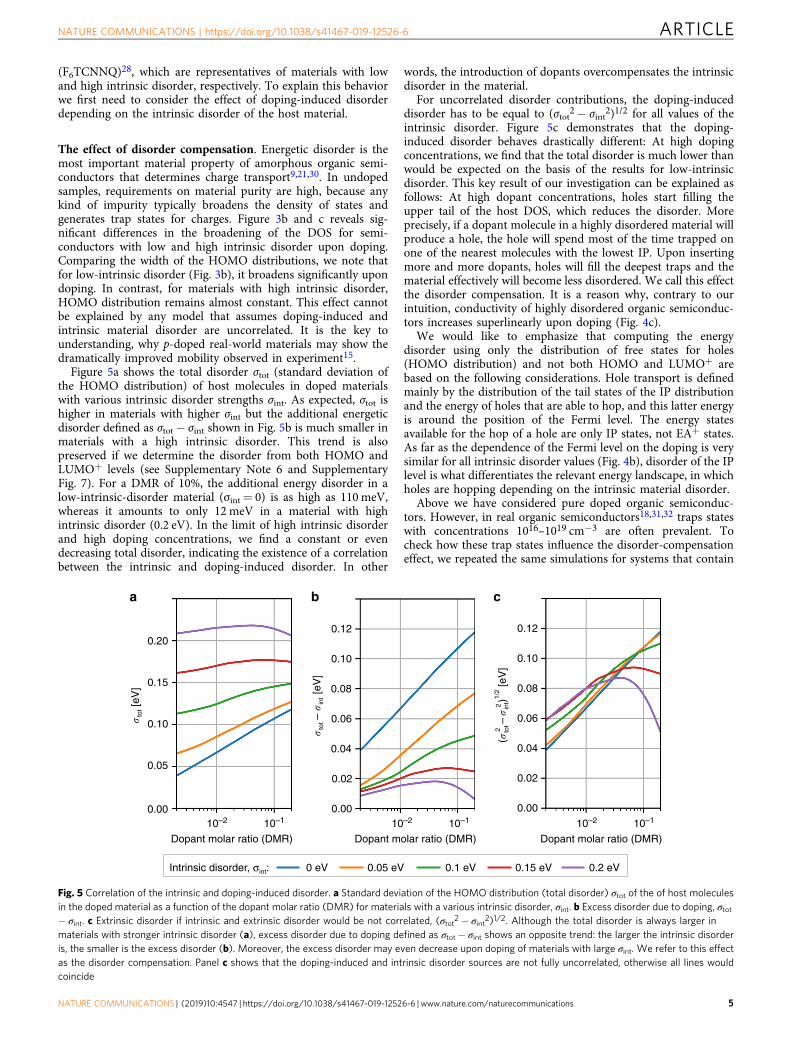
(F6TCNNQ)28, which are representatives of materials with lowand high intrinsic disorder, respectively. To explain this behaviorwe first need to consider the effect of doping-induced disorderdepending on the intrinsic disorder of the host material.
The effect of disorder compensation. Energetic disorder is themost important material property of amorphous organic semi-conductors that determines charge transport9,21,30. In undopedsamples, requirements on material purity are high, because anykind of impurity typically broadens the density of states andgenerates trap states for charges. Figure 3b and c reveals sig-nificant differences in the broadening of the DOS for semi-conductors with low and high intrinsic disorder upon doping.Comparing the width of the HOMO distributions, we note thatfor low-intrinsic disorder (Fig. 3b), it broadens significantly upondoping. In contrast, for materials with high intrinsic disorder,HOMO distribution remains almost constant. This effect cannotbe explained by any model that assumes doping-induced andintrinsic material disorder are uncorrelated. It is the key tounderstanding, why p-doped real-world materials may show thedramatically improved mobility observed in experiment15.
Figure 5a shows the total disorder σtot (standard deviation ofthe HOMO distribution) of host molecules in doped materialswith various intrinsic disorder strengths σint. As expected, σtot ishigher in materials with higher σint but the additional energeticdisorder defined as σtot− σint shown in Fig. 5b is much smaller inmaterials with a high intrinsic disorder. This trend is alsopreserved if we determine the disorder from both HOMO andLUMO+ levels (see Supplementary Note 6 and SupplementaryFig. 7). For a DMR of 10%, the additional energy disorder in alow-intrinsic-disorder material (σint= 0) is as high as 110meV,whereas it amounts to only 12 meV in a material with highintrinsic disorder (0.2 eV). In the limit of high intrinsic disorderand high doping concentrations, we find a constant or evendecreasing total disorder, indicating the existence of a correlationbetween the intrinsic and doping-induced disorder. In other
words, the introduction of dopants overcompensates the intrinsicdisorder in the material.
For uncorrelated disorder contributions, the doping-induceddisorder has to be equal to (σtot2− σint2)1/2 for all values of theintrinsic disorder. Figure 5c demonstrates that the doping-induced disorder behaves drastically different: At high dopingconcentrations, we find that the total disorder is much lower thanwould be expected on the basis of the results for low-intrinsicdisorder. This key result of our investigation can be explained asfollows: At high dopant concentrations, holes start filling theupper tail of the host DOS, which reduces the disorder. Moreprecisely, if a dopant molecule in a highly disordered material willproduce a hole, the hole will spend most of the time trapped onone of the nearest molecules with the lowest IP. Upon insertingmore and more dopants, holes will fill the deepest traps and thematerial effectively will become less disordered. We call this effectthe disorder compensation. It is a reason why, contrary to ourintuition, conductivity of highly disordered organic semiconduc-tors increases superlinearly upon doping (Fig. 4c).
We would like to emphasize that computing the energydisorder using only the distribution of free states for holes(HOMO distribution) and not both HOMO and LUMO+ arebased on the following considerations. Hole transport is definedmainly by the distribution of the tail states of the IP distributionand the energy of holes that are able to hop, and this latter energyis around the position of the Fermi level. The energy statesavailable for the hop of a hole are only IP states, not EA+ states.As far as the dependence of the Fermi level on the doping is verysimilar for all intrinsic disorder values (Fig. 4b), disorder of the IPlevel is what differentiates the relevant energy landscape, in whichholes are hopping depending on the intrinsic material disorder.
Above we have considered pure doped organic semiconduc-tors. However, in real organic semiconductors18,31,32 traps stateswith concentrations 1016–1019 cm−3 are often prevalent. Tocheck how these trap states influence the disorder-compensationeffect, we repeated the same simulations for systems that contain
0 eVIntrinsic disorder, σ :int 0.05 eV 0.1 eV 0.15 eV 0.2 eV
0.20
0.15
0.10
0.05
0.0010–2 10–1 10–2 10–1 10–2 10–1
0.12
0.10
0.08
0.06
0.04
0.02
0.00
0.12
0.10
0.08
0.06
0.04
0.02
0.00
� [e
V]
tot
��
[eV
]–
tot
int
a b c
Dopant molar ratio (DMR) Dopant molar ratio (DMR) Dopant molar ratio (DMR)
1/2
(� –
�)
[eV
]to
tin
t22
Fig. 5 Correlation of the intrinsic and doping-induced disorder. a Standard deviation of the HOMO distribution (total disorder) σtot of the of host moleculesin the doped material as a function of the dopant molar ratio (DMR) for materials with a various intrinsic disorder, σint. b Excess disorder due to doping, σtot− σint. c Extrinsic disorder if intrinsic and extrinsic disorder would be not correlated, (σtot2− σint2)1/2. Although the total disorder is always larger inmaterials with stronger intrinsic disorder (a), excess disorder due to doping defined as σtot− σint shows an opposite trend: the larger the intrinsic disorderis, the smaller is the excess disorder (b). Moreover, the excess disorder may even decrease upon doping of materials with large σint. We refer to this effectas the disorder compensation. Panel c shows that the doping-induced and intrinsic disorder sources are not fully uncorrelated, otherwise all lines wouldcoincide
NATURE COMMUNICATIONS | https://doi.org/10.1038/s41467-019-12526-6 ARTICLE
NATURE COMMUNICATIONS | (2019) 10:4547 | https://doi.org/10.1038/s41467-019-12526-6 | www.nature.com/naturecommunications 5

trap states (see Supplementary Note 7 and Supplementary Fig. 8).Our simulations revealed that trap filling is the dominant effect atultralow dopant molar ratios (DMR < 10−3), whereas thedisorder-compensation effect determines the slope of theconductivity increase in a moderate doping regime (10−3 <DMR < 10−1).
Extrinsic trap filling reported in the literature and the effectreported here are different not only in terms of doping regimeswhere they are observed. The disorder-compensation effectmeans that the increase of the electrostatic disorder due todoping is compensated by the filling of the deepest Coulombtraps, which tends to decrease the total material disorder. Itoccurs when Coulomb traps have different depth, which is onlypossible in intrinsically disordered materials. Then a hole fills thedeep state of the intrinsic material and the Coulomb trap due todopant anion. As a result, the total energetic disorder in materialswith already high intrinsic disorder may stay the same or evendecrease upon doping. In its turn, the effect of the extrinsic trapfilling is the filling of deep or shallow extrinsic states due toimpurities, rather than (ionized) dopant molecules. The trapsfilled in this latter case are not of Coulombic nature.
DiscussionTo summarize, the computation of the DOS of doped organicsemiconductors by explicit simulation of carriers and theirinteractions at a microscopic and fully correlated level demon-strates that the observed modification of the DOS does not needthe postulation of impurity-induced trap states as argued inearlier models18 to explain the experimentally observed Fermilevel shifts upon doping25–27 (Fig. 4b). More recent modelsassumed that doping-induced intergap states are caused byICTCs, which are separated from the reference energy level(HOMO) by the average Coulomb interaction of the CTstate13,14. Here we show that in addition to the Coulomb inter-action in ICTCs, additional shifts of the same order of magnitudearise due to the entropy and energetic disorder (Fig. 1c), whichinfluences the position of the doping-induced intergap states.Finally, our main finding changes the general view on the inter-play of intrinsic and doping-induced disorder that were pre-viously assumed to be uncorrelated14. Our simulationsdemonstrate that intrinsic and doping-induced disorder cannotbe considered as separate uncorrelated effects in organic semi-conductors, but modify the DOS as the result of a complexinterplay of carriers in their energetic landscape (Fig. 5a–c). Thisdisorder-compensation effect explains the observed increase ofthe average carrier mobility in organic semiconductors16, despitethe introduction of doping as another source of energetic dis-order. Note that this superlinear conductivity trend may beexplained by two scenarios: either all carriers become moremobile on average, or the fraction of the mobile carriers increases.
Due to disorder compensation, the conductivity of dopedorganic materials is much less sensitive to the degree of intrinsicdisorder of the host material (see Fig. 4c). This significantlybroadens the materials space of appropriate host molecules andthus enables the design of novel doped hole/electron transportlayers, which are ubiquitously used in most organic electronicsdevices, ranging from highly-efficient organic light-emittingdiodes to organic transistors.
MethodsTypes of simulated systems. Two types of the systems have been simulated usingkinetic Monte-Carlo method: “bulk semiconductor” and “single-layer device”.“Bulk semiconductor” is a simple cubic lattice with Nx ×Ny ×Nz sites and a latticeconstant of a= 1 nm. Each site represents the center of a mass of an organicmolecule (either host or dopant). Periodic boundary conditions (PBCs) are appliedin all spatial directions, x, y, and z. “Single-layer device” is a bulk system describedabove sandwiched between two electrodes. It differs from the first system in several
regards: first, PBCs are applied only in y and z directions; second, each electrode ismodelled by Ny ×Nz square lattice sites attached to the bulk semiconductor systemfrom the left and right at a distance of 1 nm. Electrostatic interactions are takeninto account using the Ewald summation method33 as described in Casalegnoet al.34. Electrodes are assumed to be a perfect metal, therefore, mirror charges arecreated by all particles in the system.
Details of kinetic Monte-Carlo simulations. We consider a model of p-dopedorganic semiconductor at 300 K with relative permittivity ε= 4 where molecularsites are mapped to a cubic lattice with a lattice spacing and electron/hole locali-zation radius 1 nm. Dopant molecules randomly substitute host molecules. Ourmodel includes the following microscopic processes: hopping of charges betweentwo adjacent molecules of one kind, dopant ionization and reciprocal process ofdopant neutralization; injection of polarons from electrodes and a reciprocalprocess of the polaron ejection, all of which are described by Miller-Abrahamsrates35 with an attempt frequency 2 × 10⁹ sec−1 (see Supplementary Note 1 and 2).In simulating electrical conductivity, the field of 0.04 V nm−1 is applied.
Details of numerical implementation. In all simulations, we have used 50 replicasfor each set of material/simulation parameters, and results that we present areaverages over these replicas. “Critical” sizes of a replica Nx ×Ny ×Nz that is theminimal sizes that yield the same results as systems with larger sizes have beenfound for three dopant molar ratios (10−3, 10−2, 10−1) and each disorder mag-nitude and then extrapolated for the rest of simulations. To control the con-vergence upon increasing the system size, we used mean and standard deviation ofthe HOMO and LUMO+ distributions. As a result we have found that systems withsizes up to 150 × 150 × 150 sites has to be used for low dopant concentration(DMR= 10−3) and only down to 20 × 20 × 20 sites is required for a very highdopant concentrations (DMR= 0.3). To calculate equilibrium quantities such asDOS and derived quantities (Fermi level) we have modified kMC method. Namely,in dealing with “bulk semiconductor” systems, we set the inverse localization radiusin the Miller-Abrahams equation, b−1, to zero and connect each site to its 26nearest neighbors. This allowed us to achieve equilibrium after 105 kMC steps, ascompared to 106–108 kMC steps if using realistic value of b (~1 nm−1). Settingrates in this fashion influences the time scale of the kMC simulation, but fulfills thedetailed balance principle and thus does not change the equilibrium distribution.This has been explicitly justified.
Data availabilityAll the data supporting the findings of this study are available within the article, itsSupplementary Information files, or from the corresponding author upon reasonablerequest.
Code availabilityUpon reasonable request, the authors will provide an academic single-user trial license ofLightForge for the purpose to reproduce the results of this paper.
Received: 8 May 2019; Accepted: 17 September 2019;
References1. Lüssem, B., Riede, M. & Leo, K. Doping of organic semiconductors. Phys.
Status Solidi A 210, 9–43 (2013).2. Lüssem, B. et al. Doped organic transistors. Chem. Rev. 116, 13714–13751
(2016).3. Sze, S. M. & Ng, K. K. Physics of semiconductor devices. (Wiley-Interscience,
2007).4. Blochwitz, J., Pfeiffer, M., Fritz, T. & Leo, K. Low voltage organic light emitting
diodes featuring doped phthalocyanine as hole transport material. Appl. Phys.Lett. 73, 729–731 (1998).
5. Yamamori, A., Adachi, C., Koyama, T. & Taniguchi, Y. Doped organic lightemitting diodes having a 650-nm-thick hole transport layer. Appl. Phys. Lett.72, 2147–2149 (1998).
6. Walzer, K., Maennig, B., Pfeiffer, M. & Leo, K. Highly efficient organic devicesbased on electrically doped transport layers. Chem. Rev. 107, 1233–1271(2007).
7. Jacobs, I. E. & Moulé, A. J. Controlling molecular doping in organicsemiconductors. Adv. Mater. 1703063. https://doi.org/10.1002/adma.201703063 (2017).
8. Salzmann, I., Heimel, G., Oehzelt, M., Winkler, S. & Koch, N. Molecularelectrical doping of organic semiconductors: fundamental mechanisms andemerging dopant design rules. Acc. Chem. Res. 49, 370–378 (2016).
9. Arkhipov, V. I., Heremans, P., Emelianova, E. V. & Bässler, H. Effect of dopingon the density-of-states distribution and carrier hopping in disordered organic
ARTICLE NATURE COMMUNICATIONS | https://doi.org/10.1038/s41467-019-12526-6
6 NATURE COMMUNICATIONS | (2019) 10:4547 | https://doi.org/10.1038/s41467-019-12526-6 | www.nature.com/naturecommunications

semiconductors. Phys. Rev. B 71, 045214. https://journals.aps.org/prb/abstract/10.1103/PhysRevB.71.045214 (2005).
10. Mityashin, A. et al. Unraveling the mechanism of molecular doping in organicsemiconductors. Adv. Mater. 24, 1535–1539 (2012).
11. Winkler, S. et al. Probing the energy levels in hole-doped molecularsemiconductors. Mater. Horiz. 2, 427–433 (2015).
12. Zuo, G., Abdalla, H. & Kemerink, M. Impact of doping on the density ofstates and the mobility in organic semiconductors. Phys. Rev. B 93, 235203.https://journals.aps.org/prb/abstract/10.1103/PhysRevB.93.235203 (2016).
13. Tietze, M. L. et al. Elementary steps in electrical doping of organicsemiconductors. Nat. Commun. 9, 1182. https://www.nature.com/articles/s41467-018-03302-z (2018).
14. Gaul, C. et al. Insight into doping efficiency of organic semiconductors fromthe analysis of the density of states in n-doped C60 and ZnPc. Nat. Mater. 17,439–444 (2018).
15. Schwarze, M. et al. Molecular parameters responsible for thermally activatedtransport in doped organic semiconductors. Nat. Mater. 18, 242–248 (2019).
16. Menke, T., Ray, D., Meiss, J., Leo, K. & Riede, M. In-situ conductivity andSeebeck measurements of highly efficient n-dopants in fullerene C 60. Appl.Phys. Lett. 100, 093304 (2012).
17. Symalla, F. et al. Charge transport by superexchange in molecular host-guestsystems. Phys. Rev. Lett. 117, 276803 (2016).
18. Tietze, M. L., Pahner, P., Schmidt, K., Leo, K. & Lüssem, B. Doped organicsemiconductors: trap-filling, impurity saturation, and reserve regimes. Adv.Funct. Mater. 25, 2701–2707 (2015).
19. Yang, J.-P. et al. Quantitative Fermi level tuning in amorphous organicsemiconductor by molecular doping: toward full understanding of the dopingmechanism. Appl. Phys. Lett. 109, 093302 (2016).
20. Bässler, H. Charge transport in disordered organic photoconductors a montecarlo simulation study. Phys. Status Solidi B 175, 15–56 (1993).
21. Fishchuk, I. I. et al. Unified description for hopping transport in organicsemiconductors including both energetic disorder and polaroniccontributions. Phys. Rev. B 88, 125202 (2013).
22. Liu, B. et al. High-performance doping-free hybrid white organic light-emitting diodes: the exploitation of ultrathin emitting nanolayers (<1 nm).Nano Energy 26, 26–36 (2016).
23. Kordt, P. et al. Modeling of organic light emitting diodes: from molecular todevice properties. Adv. Funct. Mater. 25, 1955–1971 (2015).
24. Friederich, P. et al. Toward design of novel materials for organic electronics.Adv. Mater. 31, 1808256. https://doi.org/10.1002/adma.201808256 (2019).
25. Olthof, S., Tress, W., Meerheim, R., Lüssem, B. & Leo, K. Photoelectronspectroscopy study of systematically varied doping concentrations in anorganic semiconductor layer using a molecular p-dopant. J. Appl. Phys. 106,103711 (2009).
26. Zhang, F. & Kahn, A. Investigation of the high electron affinity moleculardopant F6-TCNNQ for hole-transport materials. Adv. Funct. Mater. 28,1703780 (2018).
27. Tietze, M. L., Burtone, L., Riede, M., Lüssem, B. & Leo, K. Fermi level shift anddoping efficiency in p-doped small molecule organic semiconductors: Aphotoelectron spectroscopy and theoretical study. Phys. Rev. B 86, 035320(2012).
28. Menke, T. Molecular Doping of Organic Semiconductors: A Conductivity andSeebeck Study. (TU Dresden, 2013).
29. Lin, X. et al. Impact of a low concentration of dopants on the distribution ofgap states in a molecular semiconductor. Chem. Mater. 28, 2677–2684 (2016).
30. Friederich, P., Coehoorn, R. & Wenzel, W. Molecular origin of the anisotropicdye orientation in emissive layers of organic light emitting diodes. Chem.Mater. 29, 9528–9535 (2017).
31. Zhang, Y., de Boer, B. & Blom, P. W. M. Trap-free electron transport in poly(p-phenylene vinylene) by deactivation of traps with n -type doping. Phys. Rev. B81, 085201 (2010).
32. Olthof, S. et al. Ultralow doping in organic semiconductors: evidence of trapfilling. Phys. Rev. Lett. 109, 176601 (2012).
33. Ewald, P. P. Die Berechnung optischer und elektrostatischer Gitterpotentiale.Ann. Phys. 369, 253–287 (1921).
34. Casalegno, M., Raos, G. & Po, R. Methodological assessment of kinetic MonteCarlo simulations of organic photovoltaic devices: The treatment ofelectrostatic interactions. J. Chem. Phys. 132, 094705 (2010).
35. Miller, A. & Abrahams, E. Impurity conduction at low concentrations. Phys.Rev. 120, 745–755 (1960).
AcknowledgementsA.F. and W.W. received funding from the European Union Horizon 2020 research andinnovation programme under grant agreement no. 646176 (EXTMOS). P.F. receivedfunding from the European Union Horizon 2020 research and innovation programmeunder the Marie Skłodowska-Curie grant agreement No 795206. This work was per-formed on the supercomputer ForHLR-II funded by the Ministry of Science, Researchand the Arts Baden-Württemberg and by the Federal Ministry of Education andResearch. We acknowledge support by the KIT-Publication Fund of the KarlsruheInstitute of Technology.
Author contributionsA.F., P.F., and W.W. conceived and designed the project. F.S., developed and employedthe methodology to simulate doped organic materials in LightForge kMC, a multi-purpose kinetic Monte-Carlo package, A.F., did the simulations and extracted the rele-vant materials properties. All authors contributed to preparation of the manuscript. A.F.,P.F., and W.W. wrote the manuscript.
Competing interestsW.W. holds shares of a KIT spinoff, Nanomatch GmbH, which markets softwaredeveloped by KIT. The other authors declare no competing interests.
Additional informationSupplementary information is available for this paper at https://doi.org/10.1038/s41467-019-12526-6.
Correspondence and requests for materials should be addressed to W.W.
Peer review information Nature Communications thanks Karin Zojer and the other,anonymous, reviewer(s) for their contribution to the peer review of this work. Peerreviewer reports are available
Reprints and permission information is available at http://www.nature.com/reprints
Publisher’s note Springer Nature remains neutral with regard to jurisdictional claims inpublished maps and institutional affiliations.
Open Access This article is licensed under a Creative CommonsAttribution 4.0 International License, which permits use, sharing,
adaptation, distribution and reproduction in any medium or format, as long as you giveappropriate credit to the original author(s) and the source, provide a link to the CreativeCommons license, and indicate if changes were made. The images or other third partymaterial in this article are included in the article’s Creative Commons license, unlessindicated otherwise in a credit line to the material. If material is not included in thearticle’s Creative Commons license and your intended use is not permitted by statutoryregulation or exceeds the permitted use, you will need to obtain permission directly fromthe copyright holder. To view a copy of this license, visit http://creativecommons.org/licenses/by/4.0/.
© The Author(s) 2019
NATURE COMMUNICATIONS | https://doi.org/10.1038/s41467-019-12526-6 ARTICLE
NATURE COMMUNICATIONS | (2019) 10:4547 | https://doi.org/10.1038/s41467-019-12526-6 | www.nature.com/naturecommunications 7