directpath™ , pop-free3vrms line driver with adjustable gain
TRANSCRIPT

DRV602
LEFT
RIGHT-
+
-
+
DAC
DAC
SOC
DRV602
www.ti.com SLOS572D –DECEMBER 2008–REVISED OCTOBER 2010
DirectPath™, Pop-Free 3Vrms Line Driver with Adjustable GainCheck for Samples: DRV602
Designed using TI's patented DirectPath™1FEATURES
technology, the DRV602 is capable of driving 3Vrms234• DirectPath™
into a 2.5kΩ load with 5V supply voltage. The device– Eliminates Pop/Clicks has differential inputs and uses external gain setting
resistors, that supports a gain range of ±1V/V to– Eliminates Output DC-Blocking Capacitors±10V/V. The use of external gain resistors also allows– Provides Flat Frequency Responsethe implementation of a 2nd order low pass filter to20Hz–20kHzcompliment DAC's and SOC converters. The line
• Low Noise and THD output of the DRV602 has ±8kV IEC ESD protection.The DRV602 (referred to as the '602) has built-in– SNR > 102 dBshutdown control for pop-free on/off control.– Typical VN < 15 mVmsUsing the DRV602 in audio products can reduce– THD+N < 0.05% 20 Hz–20 kHzcomponent count compared to traditional methods of• Output Voltage into 2.5-kΩ Loadgenerating a 3Vrms output. The DRV602 doesn't
– 2 Vrms with 3.3-V Supply Voltage require a power supply greater than 5V to generateits 8.5VPP output, nor does it require a split rail power– 3 Vrms with 5-V Supply Voltagesupply. The DRV602 integrates its own charge pump• 3Vrms Output Voltage into 2.5 kΩ Load Withto generate a negative supply rail that provides a5V Supply Voltageclean, pop-free ground biased 3Vrms output.
• Differential InputThe DRV602 is available in a 14 pin TSSOPpackage.APPLICATIONSIf higher SNR, trimmed DC-offset and external• Set-Top Boxesundervoltage-mute functions are beneficial in the• PDP / LCD TVapplication, TI recommends the footprint compatible• Blu-ray Disc™, DVD-Players DRV603 (SLOS617).
• Home Theater in a BoxFor a stereo line and stereo HP driver see DRV604(SLOS659).DESCRIPTION
The DRV602PW is a 3Vrms pop-free stereo linedriver designed to allow the removal of the outputdc-blocking capacitors for reduced component countand cost. The device is ideal for single supplyelectronics where size and cost are critical designparameters.
1
Please be aware that an important notice concerning availability, standard warranty, and use in critical applications of TexasInstruments semiconductor products and disclaimers thereto appears at the end of this data sheet.
2DirectPath, TI FilterPro are trademarks of Texas Instruments.3Blu-ray Disc is a trademark of Blu-ray Disc Association.4All other trademarks are the property of their respective owners.
PRODUCTION DATA information is current as of publication date. Copyright © 2008–2010, Texas Instruments IncorporatedProducts conform to specifications per the terms of the TexasInstruments standard warranty. Production processing does notnecessarily include testing of all parameters.
1+INR
2
3
4
-INR
OUTR
SGND
5
6
7 8
EN
PVSS
CN
9
10
11
12
13
14
CP
PVDD
PGND
OUTL
-INL
+INL
Charge Pump
NC
a
DRV602
SLOS572D –DECEMBER 2008–REVISED OCTOBER 2010 www.ti.com
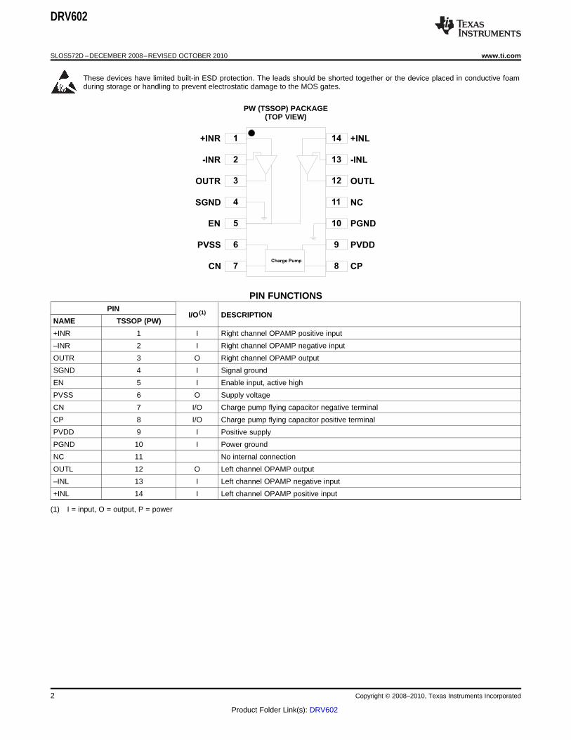
These devices have limited built-in ESD protection. The leads should be shorted together or the device placed in conductive foamduring storage or handling to prevent electrostatic damage to the MOS gates.
PW (TSSOP) PACKAGE(TOP VIEW)
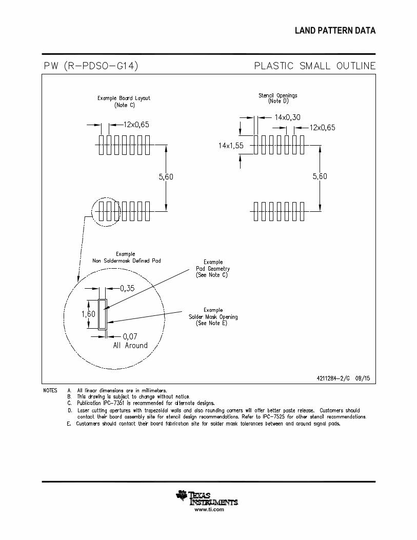
PIN FUNCTIONSPIN
I/O (1) DESCRIPTIONNAME TSSOP (PW)
+INR 1 I Right channel OPAMP positive input
–INR 2 I Right channel OPAMP negative input
OUTR 3 O Right channel OPAMP output
SGND 4 I Signal ground
EN 5 I Enable input, active high
PVSS 6 O Supply voltage
CN 7 I/O Charge pump flying capacitor negative terminal
CP 8 I/O Charge pump flying capacitor positive terminal
PVDD 9 I Positive supply
PGND 10 I Power ground
NC 11 No internal connection
OUTL 12 O Left channel OPAMP output
–INL 13 I Left channel OPAMP negative input
+INL 14 I Left channel OPAMP positive input
(1) I = input, O = output, P = power
2 Copyright © 2008–2010, Texas Instruments Incorporated
Product Folder Link(s): DRV602

DRV602
www.ti.com SLOS572D –DECEMBER 2008–REVISED OCTOBER 2010
ABSOLUTE MAXIMUM RATINGS (1) (2)
over operating free-air temperature rangeVALUE UNIT
Supply voltage, VDD to GND –0.3 V to 5.5 V
VI Input voltage VSS – 0.3 to VDD + 0.3 V
RL Minimum load impedance > 600 ΩEN to GND –0.3 to VDD +0.3 V
TJ Maximum operating junction temperature range, –40 to 150 °C
Tstg Storage temperature range –40 to 150 °C
ESD IEC Contact ESD Protection per IEC6100-4-2, on output pins measured on DRV602EVM ±8 kV
(1) Stresses beyond those listed under absolute maximum ratings may cause permanent damage to the device. These are stress ratingsonly, and functional operation of the device at these or any other conditions beyond those indicated under recommended operatingconditions is not implied. Exposure to absolute-maximum-rated conditions for extended periods may affect device reliability.
(2) These voltages represents the DC voltage + peak AC waveform measured at the terminal of the device in all conditions.
DISSIPATION RATINGSPOWER RATING (1) POWER RATING (1)
PACKAGE qJC (°/W) qJA (°/W) AT TA ≤ 25°C AT TA ≤ 70°C
TSSOP-14 (PW) 35 115 (2) 870mW 348mW
(1) Power rating is determined with a junction temperature of 125°C. This is the point where performance starts to degrade and long-termreliability starts to be reduced. Thermal management of the final PCB should strive to keep the junction temperature at or below 125°Cfor best performance and reliability.
(2) These data were taken with the JEDEC High-K test printed circuit board (PCB). For the JEDEC low-K test PCB, the qJA is 185°C.
ORDERING INFORMATIONTA PACKAGE (1) DESCRIPTION
-40°C to 85°C DRV602PW 14-Pin TSSOP
(1) For the most current package and ordering information, see the Package Option Addendum at the end of this document, or see the TIwebsite at www.ti.com.
RECOMMENDED OPERATING CONDITIONSMIN TYP MAX UNIT
VDD Supply voltage, DC Supply Voltage 3 3.3 5.5 V
VIH High-level input voltage EN 60 % of VDD
VIL Low-level input voltage EN 40 % of VDD
TA Operating free-air temperature –40 85 °C
ELECTRICAL CHARACTERISTICSTA = 25°C (unless otherwise noted)
PARAMETER TEST CONDITIONS MIN TYP MAX UNIT
|VOS| Output offset voltage VDD = 3 V to 5 V, Voltage follower - gain = 1 5 mV
PSRR Supply Rejection Ratio VDD = 3.3 V to 5 V 88 dB
VOH High-level output voltage VDD = 3.3 V, RL = 2.5 kΩ 3.10 V
VOL Low-level output voltage VDD = 3.3 V, RL = 2.5 kΩ –3.05 V
|IIH| High-level input current (EN) VDD = 5 V, VI = VDD 1 µA
|IIL| Low-level input current (EN) VDD = 5 V, VI = 0 V 1 µA
VDD = 3.3 V, No load, EN = VDD 8 11mA
IDD Supply Current VDD = 5 V, No load, EN = VDD 12.5 20
Shutdown mode, Vdd = 3 V to 5 V 2 mA
Copyright © 2008–2010, Texas Instruments Incorporated 3
Product Folder Link(s): DRV602
R3
C2
RIGHT
INPUT
+
-
LEFT
INPUT
LEFT
OUTPUT
RIGHT
OUTPUT
3.3V
supply
C1
C2
R3
R2
R2
R1
R1
R3+
-
C1R3R1
R1
R2 C2
R2
C31 Fm
DR
V602
1 Fm
1 Fm
Click a
nd
Po
p
Su
pp
ressio
n
Sh
ort
Cir
cu
it
Pro
tecti
on
SG
ND
Bia
s
Cir
cu
itry
PV
SS
CN
CP
PV
DD
-IN
L
+IN
L
OU
TR
-IN
R
OU
TL
+IN
R
EN
PG
ND
NC
Lin
e
Dri
ver
Lin
eD
river
C2ENABLE
C3
C3
C3
DRV602
SLOS572D –DECEMBER 2008–REVISED OCTOBER 2010 www.ti.com
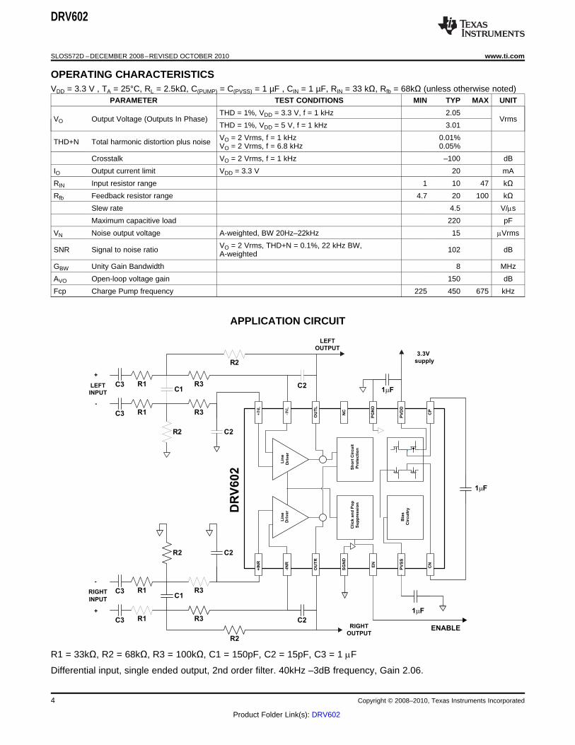
OPERATING CHARACTERISTICSVDD = 3.3 V , TA = 25°C, RL = 2.5kΩ, C(PUMP) = C(PVSS) = 1 µF , CIN = 1 µF, RIN = 33 kΩ, Rfb = 68kΩ (unless otherwise noted)
PARAMETER TEST CONDITIONS MIN TYP MAX UNIT
THD = 1%, VDD = 3.3 V, f = 1 kHz 2.05VO Output Voltage (Outputs In Phase) Vrms
THD = 1%, VDD = 5 V, f = 1 kHz 3.01
VO = 2 Vrms, f = 1 kHz 0.01%THD+N Total harmonic distortion plus noise VO = 2 Vrms, f = 6.8 kHz 0.05%
Crosstalk VO = 2 Vrms, f = 1 kHz –100 dB
IO Output current limit VDD = 3.3 V 20 mA
RIN Input resistor range 1 10 47 kΩRfb Feedback resistor range 4.7 20 100 kΩ
Slew rate 4.5 V/ms
Maximum capacitive load 220 pF
VN Noise output voltage A-weighted, BW 20Hz–22kHz 15 mVrms
VO = 2 Vrms, THD+N = 0.1%, 22 kHz BW,SNR Signal to noise ratio 102 dBA-weighted
GBW Unity Gain Bandwidth 8 MHz
AVO Open-loop voltage gain 150 dB
Fcp Charge Pump frequency 225 450 675 kHz
APPLICATION CIRCUIT
R1 = 33kΩ, R2 = 68kΩ, R3 = 100kΩ, C1 = 150pF, C2 = 15pF, C3 = 1 mF
Differential input, single ended output, 2nd order filter. 40kHz –3dB frequency, Gain 2.06.
4 Copyright © 2008–2010, Texas Instruments Incorporated
Product Folder Link(s): DRV602
0.0001
10
0.001
0.01
0.1
1
5
100m 5200m 500m 800m 2 3 4V - Output Voltage - VrmsO
TH
D+
N -
To
tal H
arm
on
ic D
isto
rtio
n+
No
ise -
%
20 Hz
1 kHz
6.7 kHz
20 20k50 100 200 500 1k 2k 5k
0.0001
10
0.001
0.01
0.1
1
5
TH
D+
N -
To
tal
Ha
rmo
nic
Dis
tort
ion
+N
ois
e -
%
f - Frequency - Hz
200 mVrms
2 Vrms
14m
12m
10m
8m
6m
4m
2m
0-0 +1 +2 +3 +4 +5
Qu
iescen
t C
urr
en
t -
A
V - Supply Voltage - VDD
No Load,V = 0 VI
+0
-20
-40
-60
-80
-100
-120
-140
0 5k 10k 20k15k
V = 2VrmsO
FF
T -
dB
r
f - Frequency - Hz
DRV602
www.ti.com SLOS572D –DECEMBER 2008–REVISED OCTOBER 2010
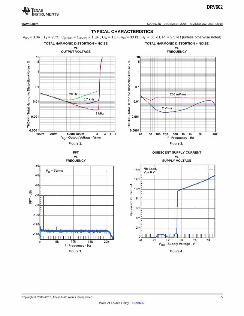
TYPICAL CHARACTERISTICSVDD = 3.3V , TA = 25°C, C(PUMP) = C(PVSS) = 1 µF , CIN = 1 µF, RIN = 33 kΩ, Rfb = 68 kΩ, RL = 2.5 kΩ (unless otherwise noted)
TOTAL HARMONIC DISTORTION + NOISE TOTAL HARMONIC DISTORTION + NOISEvs vs
OUTPUT VOLTAGE FREQUENCY
Figure 1. Figure 2.
FFT QUIESCENT SUPPLY CURRENTvs vs
FREQUENCY SUPPLY VOLTAGE
Figure 3. Figure 4.
Copyright © 2008–2010, Texas Instruments Incorporated 5
Product Folder Link(s): DRV602

OPAMP
Co
Mute Circuit
Output
Enable
+
+
+
-
Conventional Solution
DRV602Output
Enable
+
-
DVR602 Solution
VDD
VSS
GND
VDD
VDD/2
GND
DirectPath
9-12 V
5 V
DRV602
SLOS572D –DECEMBER 2008–REVISED OCTOBER 2010 www.ti.com
APPLICATION INFORMATION
Line Driver Amplifiers
Single-supply line driver amplifiers typically require dc-blocking capacitors. The top drawing in Figure 5 illustratesthe conventional line driver amplifier connection to the load and output signal.
DC blocking capacitors are often large in value, and a mute circuit is needed during power up to minimize click &pop. The output capacitor and mute circuit consume PCB area and increase cost of assembly, and can reducethe fidelity of the audio output signal.
Figure 5. Conventional and DirectPath Line Driver
The DirectPath™ amplifier architecture operates from a single supply, but makes use of an internal charge pumpto provide a negative voltage rail.
Combining the user provided positive rail and the negative rail generated by the IC, the device operates in whatis effectively a split supply mode.
The output voltages are now centered at zero volts with the capability to swing to the positive rail or negative rail.The DirectPath amplifier requires no output dc blocking capacitors.
The bottom block diagram and waveform of Figure 5 illustrate the ground-referenced Line Driver architecture.This is the architecture of the DRV602.
6 Copyright © 2008–2010, Texas Instruments Incorporated
Product Folder Link(s): DRV602
-In
Rfb
+
-
Inverting
RINCIN
Rfb
Rfb
+
-DifferentialInput
-In
+In
CIN RIN
RINCIN
RIN
CIN
+In
Rfb
Rx
+
-
Cx
NonInverting
DRV602
www.ti.com SLOS572D –DECEMBER 2008–REVISED OCTOBER 2010
Charge Pump Flying Capacitor and PVSS Capacitor
The charge pump flying capacitor, CPUMP, serves to transfer charge during the generation of the negative supplyvoltage. The PVSS capacitor must be at least equal to the charge pump capacitor in order to allow maximumcharge transfer. Low ESR capacitors are an ideal selection, and a value of 1µF is typical. Capacitor values thatare smaller than 1µF can be used, but the maximum output voltage may be reduced and the device may notoperate to specifications.
Decoupling Capacitors
The DRV602 is a DirectPath Line Driver amplifier that require adequate power supply decoupling to ensure thatthe noise and total harmonic distortion (THD) are low. A good low equivalent-series-resistance (ESR) ceramiccapacitor, typically 1µF, placed as close as possible to the device PVDD lead works best. Placing this decouplingcapacitor close to the DRV602 is important for the performance of the amplifier. For filtering lower frequencynoise signals, a 10-µF or greater capacitor placed near the audio power amplifier would also help, but it is notrequired in most applications because of the high PSRR of this device.
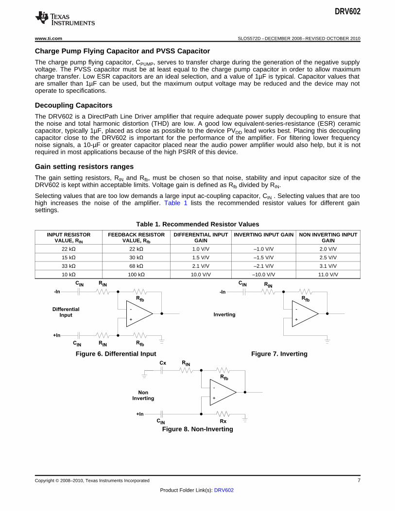
Gain setting resistors ranges
The gain setting resistors, RIN and Rfb, must be chosen so that noise, stability and input capacitor size of theDRV602 is kept within acceptable limits. Voltage gain is defined as Rfb divided by RIN.
Selecting values that are too low demands a large input ac-coupling capacitor, CIN . Selecting values that are toohigh increases the noise of the amplifier. Table 1 lists the recommended resistor values for different gainsettings.
Table 1. Recommended Resistor Values
INPUT RESISTOR FEEDBACK RESISTOR DIFFERENTIAL INPUT INVERTING INPUT GAIN NON INVERTING INPUTVALUE, RIN VALUE, Rfb GAIN GAIN
22 kΩ 22 kΩ 1.0 V/V –1.0 V/V 2.0 V/V
15 kΩ 30 kΩ 1.5 V/V –1.5 V/V 2.5 V/V
33 kΩ 68 kΩ 2.1 V/V –2.1 V/V 3.1 V/V
10 kΩ 100 kΩ 10.0 V/V –10.0 V/V 11.0 V/V
Figure 6. Differential Input Figure 7. Inverting
Figure 8. Non-Inverting
Copyright © 2008–2010, Texas Instruments Incorporated 7
Product Folder Link(s): DRV602

fcIN 1
2 RIN CINCIN
12 fcIN RIN
or
- In
Differential Input Inverting Input
DRV602
R1
R2
+
-
C3 R3 C1
C2
+ In
- In
R1
R2
+
-
C3 R3 C1
C2
C3 R1 R3 C1
R2
DRV602
DRV602
SLOS572D –DECEMBER 2008–REVISED OCTOBER 2010 www.ti.com
Input-Blocking Capacitors
DC input-blocking capacitors are required to be added in series with the audio signal into the input pins of theDRV602. These capacitors block the DC portion of the audio source and allow the DRV602 inputs to be properlybiased to provide maximum performance. The input blocking capacitors also limit the DC gain to 1, limiting theDC-offset voltage at the output.
These capacitors form a high-pass filter with the input resistor, RIN. The cutoff frequency is calculated usingEquation 1. For this calculation, the capacitance used is the input-blocking capacitor and the resistance is theinput resistor chosen from Table 1, then the frequency and/or capacitance can be determined when one of thetwo values are given.
(1)
Using the DRV602 as 2nd Order Filter
Several audio DACs used today require an external low-pass filter to remove out of band noise. This is possiblewith the DRV602 as it can be used like a standard OPAMP.
Several filter topologies can be implemented both single ended and differential. In Figure 9, a Multi FeedBack -MFB, with differential input and single ended input is shown.
An ac-coupling capacitor to remove dc-content from the source is shown, it serves to block any dc content fromthe source and lowers the dc-gain to 1 helping reducing the output dc-offset to minimum.
The component values can be calculated with the help of the TI FilterPro™ program available on the TI websiteat: http://focus.ti.com/docs/toolsw/folders/print/filterpro.html
Figure 9. 2nd Order Active Low Pass Filter
The resistor values should have a low value for obtaining low noise, but should also have a high enough value toget a small size ac-coupling cap. With the proposed values, 33k, 68k, 100k, a DNR of 102dB can be achievedwith a small 1mF input ac-coupling capacitor.
8 Copyright © 2008–2010, Texas Instruments Incorporated
Product Folder Link(s): DRV602
Supply ramp
Supply
EN
Time for ac-couplingcapacitors to charge
DRV602
www.ti.com SLOS572D –DECEMBER 2008–REVISED OCTOBER 2010
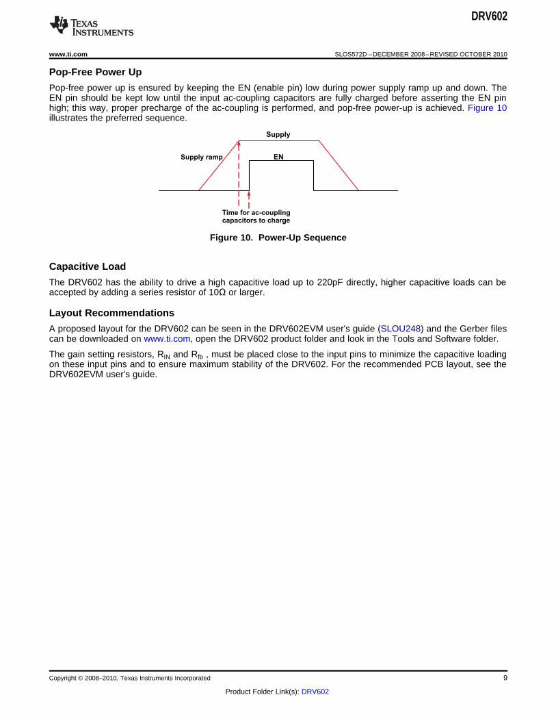
Pop-Free Power Up
Pop-free power up is ensured by keeping the EN (enable pin) low during power supply ramp up and down. TheEN pin should be kept low until the input ac-coupling capacitors are fully charged before asserting the EN pinhigh; this way, proper precharge of the ac-coupling is performed, and pop-free power-up is achieved. Figure 10illustrates the preferred sequence.
Figure 10. Power-Up Sequence
Capacitive Load
The DRV602 has the ability to drive a high capacitive load up to 220pF directly, higher capacitive loads can beaccepted by adding a series resistor of 10Ω or larger.
Layout Recommendations
A proposed layout for the DRV602 can be seen in the DRV602EVM user's guide (SLOU248) and the Gerber filescan be downloaded on www.ti.com, open the DRV602 product folder and look in the Tools and Software folder.
The gain setting resistors, RIN and Rfb , must be placed close to the input pins to minimize the capacitive loadingon these input pins and to ensure maximum stability of the DRV602. For the recommended PCB layout, see theDRV602EVM user's guide.
Copyright © 2008–2010, Texas Instruments Incorporated 9
Product Folder Link(s): DRV602
DRV602
SLOS572D –DECEMBER 2008–REVISED OCTOBER 2010 www.ti.com
REVISION HISTORY
NOTE: Page numbers of current version may differ from previous versions.
Changes from Revision A (December 2008) to Revision B Page
• Changed crosstalk spec from -80dB to -100dB .................................................................................................................... 4
Changes from Revision B (October 2009) to Revision C Page
• Added "Pop-Free" to title and changed "pop-less" to "pop-free in description text strings. ................................................. 1
• Added Output Voltage Feature bullet: "3Vrms With 5-V Supply Voltage" ............................................................................ 1
• Changed "2Vrms" to "3Vrms" in Description Section ........................................................................................................... 1
• Changed "5VPP" to "8.5VPP" in Description Section .............................................................................................................. 1
• Changed Recommended Operating Conditions TA range from "0 to 70 °C" to "–40 to 85°C" ............................................. 3
• Changed Electrical Characteristics Test Conditions VDD from "4.5 V" to "5 V" .................................................................... 3
• Added "VO" spec. for "VDD = 5 V" to Operating Characteristics table ................................................................................... 4
Changes from Revision May 2010 (C) to Revision D Page
• Changed Abs Max Table (TJ) From: -40°C to 85°C to -40°C to 150 .................................................................................... 3
• Changed RIGHT INPUT From: + / - To: - / + in the Application Circuit ................................................................................ 4
• Added RL = 2.5 kΩ to the TYPICAL CHARACTERISTICS conditions statement ................................................................ 5
• Added , CPUMP, to the first sentence of the Charge Pump Flying Capacitor and PVSS Capacitor section .......................... 7
• Changed VDD To: PVDD in Decoupling Capacitors section ................................................................................................... 7
• Changed SD (shutdown pin) to EN (enable pin) in the Pop-Free Power Up section ........................................................... 9
• Deleted last sentence in the Capacitive Load section .......................................................................................................... 9
10 Copyright © 2008–2010, Texas Instruments Incorporated
Product Folder Link(s): DRV602
PACKAGE OPTION ADDENDUM
www.ti.com 10-Dec-2020
Addendum-Page 1
PACKAGING INFORMATION
Orderable Device Status(1)
Package Type PackageDrawing
Pins PackageQty
Eco Plan(2)
Lead finish/Ball material
(6)
MSL Peak Temp(3)
Op Temp (°C) Device Marking(4/5)
Samples
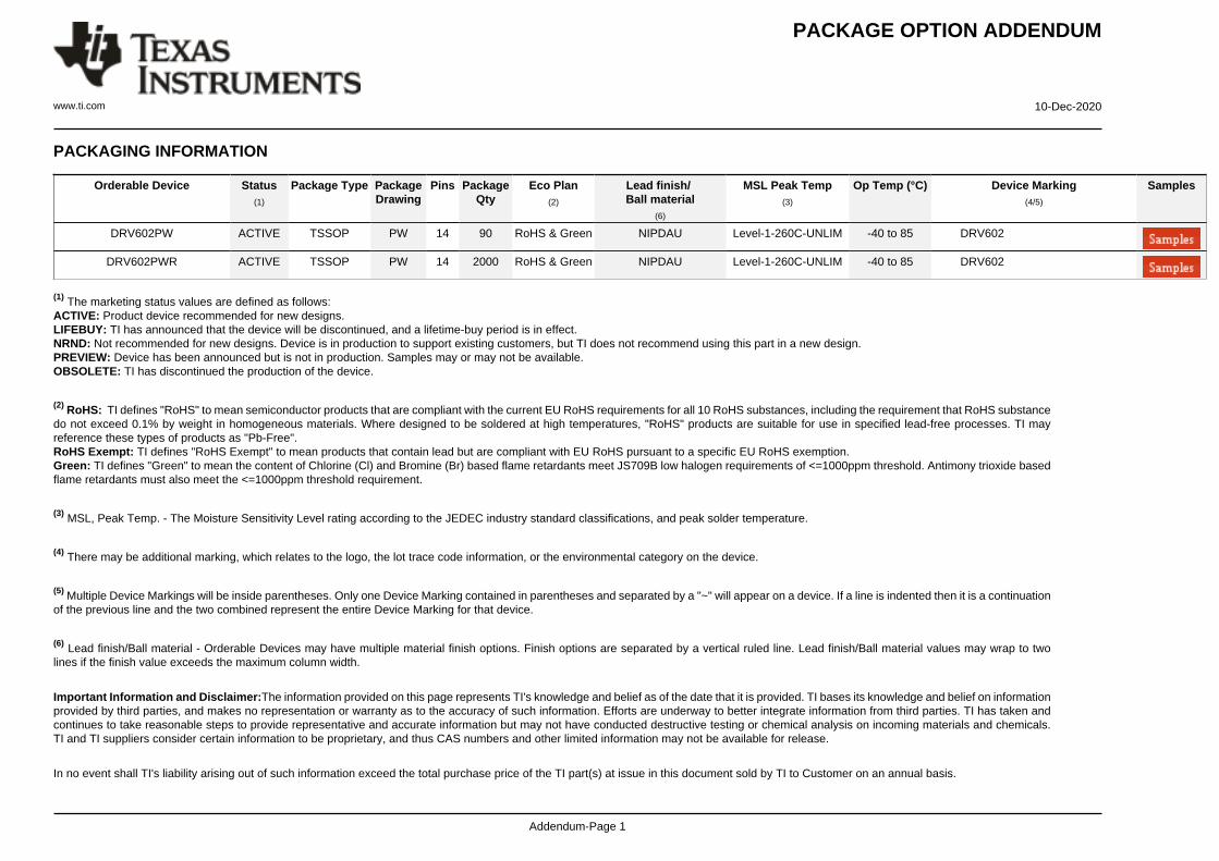
DRV602PW ACTIVE TSSOP PW 14 90 RoHS & Green NIPDAU Level-1-260C-UNLIM -40 to 85 DRV602
DRV602PWR ACTIVE TSSOP PW 14 2000 RoHS & Green NIPDAU Level-1-260C-UNLIM -40 to 85 DRV602
(1) The marketing status values are defined as follows:ACTIVE: Product device recommended for new designs.LIFEBUY: TI has announced that the device will be discontinued, and a lifetime-buy period is in effect.NRND: Not recommended for new designs. Device is in production to support existing customers, but TI does not recommend using this part in a new design.PREVIEW: Device has been announced but is not in production. Samples may or may not be available.OBSOLETE: TI has discontinued the production of the device.
(2) RoHS: TI defines "RoHS" to mean semiconductor products that are compliant with the current EU RoHS requirements for all 10 RoHS substances, including the requirement that RoHS substancedo not exceed 0.1% by weight in homogeneous materials. Where designed to be soldered at high temperatures, "RoHS" products are suitable for use in specified lead-free processes. TI mayreference these types of products as "Pb-Free".RoHS Exempt: TI defines "RoHS Exempt" to mean products that contain lead but are compliant with EU RoHS pursuant to a specific EU RoHS exemption.Green: TI defines "Green" to mean the content of Chlorine (Cl) and Bromine (Br) based flame retardants meet JS709B low halogen requirements of <=1000ppm threshold. Antimony trioxide basedflame retardants must also meet the <=1000ppm threshold requirement.
(3) MSL, Peak Temp. - The Moisture Sensitivity Level rating according to the JEDEC industry standard classifications, and peak solder temperature.
(4) There may be additional marking, which relates to the logo, the lot trace code information, or the environmental category on the device.
(5) Multiple Device Markings will be inside parentheses. Only one Device Marking contained in parentheses and separated by a "~" will appear on a device. If a line is indented then it is a continuationof the previous line and the two combined represent the entire Device Marking for that device.
(6) Lead finish/Ball material - Orderable Devices may have multiple material finish options. Finish options are separated by a vertical ruled line. Lead finish/Ball material values may wrap to twolines if the finish value exceeds the maximum column width.
Important Information and Disclaimer:The information provided on this page represents TI's knowledge and belief as of the date that it is provided. TI bases its knowledge and belief on informationprovided by third parties, and makes no representation or warranty as to the accuracy of such information. Efforts are underway to better integrate information from third parties. TI has taken andcontinues to take reasonable steps to provide representative and accurate information but may not have conducted destructive testing or chemical analysis on incoming materials and chemicals.TI and TI suppliers consider certain information to be proprietary, and thus CAS numbers and other limited information may not be available for release.
In no event shall TI's liability arising out of such information exceed the total purchase price of the TI part(s) at issue in this document sold by TI to Customer on an annual basis.

PACKAGE OPTION ADDENDUM
www.ti.com 10-Dec-2020
Addendum-Page 2
TAPE AND REEL INFORMATION
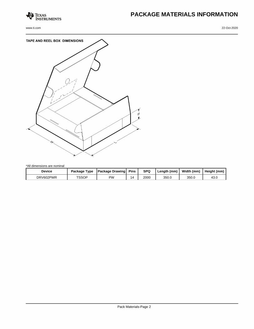
*All dimensions are nominal
Device PackageType
PackageDrawing
Pins SPQ ReelDiameter
(mm)
ReelWidth
W1 (mm)
A0(mm)
B0(mm)
K0(mm)
P1(mm)
W(mm)
Pin1Quadrant
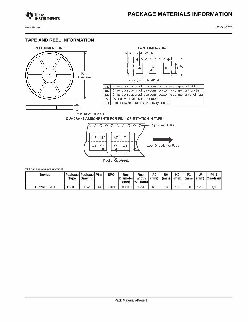
DRV602PWR TSSOP PW 14 2000 330.0 12.4 6.9 5.6 1.6 8.0 12.0 Q1
PACKAGE MATERIALS INFORMATION
www.ti.com 22-Oct-2020
Pack Materials-Page 1
*All dimensions are nominal
Device Package Type Package Drawing Pins SPQ Length (mm) Width (mm) Height (mm)
DRV602PWR TSSOP PW 14 2000 350.0 350.0 43.0
PACKAGE MATERIALS INFORMATION
www.ti.com 22-Oct-2020
Pack Materials-Page 2

IMPORTANT NOTICE AND DISCLAIMER
TI PROVIDES TECHNICAL AND RELIABILITY DATA (INCLUDING DATASHEETS), DESIGN RESOURCES (INCLUDING REFERENCE DESIGNS), APPLICATION OR OTHER DESIGN ADVICE, WEB TOOLS, SAFETY INFORMATION, AND OTHER RESOURCES “AS IS” AND WITH ALL FAULTS, AND DISCLAIMS ALL WARRANTIES, EXPRESS AND IMPLIED, INCLUDING WITHOUT LIMITATION ANY IMPLIED WARRANTIES OF MERCHANTABILITY, FITNESS FOR A PARTICULAR PURPOSE OR NON-INFRINGEMENT OF THIRD PARTY INTELLECTUAL PROPERTY RIGHTS.These resources are intended for skilled developers designing with TI products. You are solely responsible for (1) selecting the appropriate TI products for your application, (2) designing, validating and testing your application, and (3) ensuring your application meets applicable standards, and any other safety, security, or other requirements. These resources are subject to change without notice. TI grants you permission to use these resources only for development of an application that uses the TI products described in the resource. Other reproduction and display of these resources is prohibited. No license is granted to any other TI intellectual property right or to any third party intellectual property right. TI disclaims responsibility for, and you will fully indemnify TI and its representatives against, any claims, damages, costs, losses, and liabilities arising out of your use of these resources.TI’s products are provided subject to TI’s Terms of Sale (www.ti.com/legal/termsofsale.html) or other applicable terms available either on ti.com or provided in conjunction with such TI products. TI’s provision of these resources does not expand or otherwise alter TI’s applicable warranties or warranty disclaimers for TI products.
Mailing Address: Texas Instruments, Post Office Box 655303, Dallas, Texas 75265Copyright © 2020, Texas Instruments Incorporated