directional raman scattering from single molecules in...
TRANSCRIPT

Directional Raman Scattering from Single Molecules in the FeedGaps of Optical AntennasDongxing Wang,† Wenqi Zhu,† Michael D. Best,‡ Jon P. Camden,‡ and Kenneth B. Crozier*,†
†School of Engineering and Applied Sciences, Harvard University, Cambridge, Massachusetts, United States‡Department of Chemistry, University of Tennessee, Knoxville, Tennessee, United States
*S Supporting Information
ABSTRACT: Controlling light from single emitters is anoverarching theme of nano-optics. Antennas are routinely usedto modify the angular emission patterns of radio wave sources.“Optical antennas” translate these principles to visible andinfrared wavelengths and have been recently used to modifyfluorescence from single quantum dots and single molecules.Understanding the properties of single molecules, however,would be advanced were one able to observe their vibrationalspectra through Raman scattering in a very reproducible manner but it is a hugely challenging task, as Raman scattering crosssections are very weak. Here we measure for the first time the highly directional emission patterns of Raman scattering fromsingle molecules in the feed gaps of optical antennas fabricated on a chip. More than a thousand single molecule events areobserved, revealing that an unprecedented near-unity fraction of optical antennas have single molecule sensitivity.
KEYWORDS: Optical antenna, optical antenna chip, SERS enhancement, single molecule SERS, directional Raman scattering,isotopologues method
Considerable interest currently exists for techniques bywhich one can modify the light from single quantum
emitters.1,2 Optical antennas3−5 have been recently shown toenable control over the fluorescent emission from singlequantum dots6 and single molecules.7,8 It is known, however,that Raman scattering provides far richer information on theproperties of molecules than does fluorescence. Obtaining theRaman spectra of single molecules, however, is very difficult, asRaman scattering cross sections are very small.9 The drawbackof Raman scattering cross sections being weak is mitigatedusing the enhanced fields around nanostructures in the methodknown as surface-enhanced Raman scattering (SERS).10−12
Reports of single molecule SERS (SMSERS)13,14 generatedconsiderable interest but, with one notable exception,15 thosethat followed16−22 have left largely unchanged the method toproduce the SMSERS-active substrates, the salt-inducedaggregation of Ag nanoparticles. The aggregates that resultare extremely heterogeneous and generally fewer than 1% areSMSERS-active.23 The lack of reproducible substrates hashindered scientific and technological applications of SMSERS,and the realization of a controllable means for SMSERS isneeded. Ahmed and Gordon15 fabricated a single opticalantenna and reported SMSERS based on the bianalytetechnique with Rhodamine 6G and Nile Blue dyes. Here, wedemonstrate SMSERS from an optical antenna chip containingmore than a thousand optical antennas. Because of the largenumber of antennas, statistical analysis is possible and showsthat the fraction of antennas having single molecule sensitivityis near unity. That the antennas are SMSERS-active is provenusing two isotopologues of the same molecule at a
concentration that is 3 orders of magnitude lower than thatof ref 15. We furthermore directly measure the angularemission profiles of SERS at the single molecule level, showingthat directional emission is achieved.The SMSERS chip we introduce consists of a square array of
optical antennas. Figure 1a depicts a portion of the arrayschematically. Each optical antenna consists of a pair of silverparticles surrounded by a silver ring, all on a SiO2 spacer layeron a silver mirror. The silver particles are separated by a gap ofonly ∼5 nm. As a consequence, very strong field enhancementresults upon illumination of the chip with a wave polarizedacross the gap (Figure 1b). This leads to strong excitation ofRaman scattering from molecules located in the gap.The chip is made using top-down fabrication methods that
yield excellent control of the characteristics and positions of thehot spots. Device fabrication starts with a glass substrate coatedwith a layer of indium tin oxide (ITO). Silver is deposited to athickness of 120 nm by electron beam evaporation. The spaceris then produced by sputtering SiO2 to a thickness of 50 nm.Polymethylmethacrylate (PMMA) 495 and PMMA 950 arethen spun on to thicknesses of 200 and 100 nm, respectively.Electron beam lithography is then performed but only theright-hand rod of each antenna is exposed. Followingdevelopment, silver is evaporated to a thickness of 40 nmand lift-off is performed. PMMA layers are then again spun onand electron beam lithography performed. This time, an
Received: February 23, 2013Revised: March 29, 2013
Letter
pubs.acs.org/NanoLett
© XXXX American Chemical Society A dx.doi.org/10.1021/nl400698w | Nano Lett. XXXX, XXX, XXX−XXX

alignment step is performed and the left-hand rod of eachantenna and the rings are exposed. Silver is evaporated and lift-off is performed. The error in aligning the second electronbeam lithography step to the first is ±10 nm. To achieve anarray of antennas with nanometer-scale gaps, we therefore needto make several devices. We find that, roughly speaking, in oneout of six antenna arrays an alignment accuracy similar to thatof Figure 1 is achieved. We find that in such devices theantenna gap sizes vary little across the array. No gap fusionwithin the antenna array shown in Figure 1 is observed. Thefabrication method here is different from our previousmethod24 for producing nanoscale gaps in which the lateraloxidation of a Cr layer was employed. SEM images of the chipare shown as Figure 1c,d. It can be seen that the dimensions ofthe rings, gaps, and right part of optical antennas of thefabricated device match those of Figure 1a but that the left-hand rod of each antenna is slightly longer than the right-handrod. As shown in Figure S1 of the Supporting Information,however, this results in only a small change (<7%) to theintensity enhancement.The silver mirror, SiO2 spacer, and silver rings in our device
are favorable for excitation enhancement for Raman emissionenhancement and for efficient collection. The silver mirrorsupports image dipoles that couple with the localized surfaceplasmons excited on the nanoparticle pairs.25,26 The silver ringexcites surface plasmon polaritons on the mirror that convergeto the ring center,27 leading to stronger excitation of theparticle pairs. Compared with the electric field intensity (6.4 ×
103) in the middle of the gap of a basic optical antenna on SiO2(e.g., no rings and mirrors, Figure S2 of SupportingInformation), the electric field intensity (1.36 × 10⁵) in themiddle of the gap of our design in Figure 1b is ∼21 timeslarger. The simulation results (not shown here) predict that theelectric field intensity (4.5 × 10⁴) in the middle of the gap of anoptical antenna without the silver ring but above a silver mirroris ∼7 times larger than that in the middle of the gap of a basicoptical antenna. This indicates that the silver mirror and silverring improve electric field intensity enhancement by ∼7 timesand ∼3 times, respectively. We also simulate a single opticalantenna over silver mirror with the same parameters shown inFigure 1. This antenna is isolated, that is, there are noneighboring antennas. The results (not shown here) indicatethat the electric field intensity (1.29 × 10⁵) in the middle of thegap of the single antenna is close to that (1.36 × 10⁵) in themiddle of the gap of the antenna shown in Figure 1 where theneighboring antennas are taken into account. The smallvariation (6%) indicates that the interaction between theantennas is not strong in this design. In our design, thethickness of the SiO2 spacer layer25,26 and the silver ringdimensions27 are chosen to achieve optimal local fieldenhancement.Similar to the findings of previous studies,27,28 the silver
mirror and rings in the chip also collimate the Raman emission,increasing collection efficiency. To quantify the Ramanemission process, the Raman molecules are modeled as dipolesoriented in the x direction. In Figure 2a,b, the simulated far-
Figure 1. Optical antenna chip. (a) Schematic of optical antenna chip for SMSERS. Each antenna consists of pair of Ag particles (5 nm gap)surrounded by an Ag ring, all on a SiO2 spacer layer on a Ag mirror on ITO-coated glass. Ag rings have inner and outer radii of 300 and 380 nm,respectively. Ag particles and rings are 40 nm thick (in z-direction). Ag particles are rods (70 nm long and 60 nm wide in x- and y-directions) withrounded ends (30 nm radius). Periodicities of the antennas in x and y-directions are both 2 μm. (b) Profile of the simulated intensities of electricfield at the wavelength of λ=532 nm on xy plane and 20 nm above the top surface of SiO2 spacer. Intensities of electric field are normalized by that ofthe incident wave. Polarization and propagation direction of incident wave are given in Figure 1a. Dashed lines indicate outlines of silver ring andparticle pair. Inset: intensities of electric field around particle pair. (c,d) Scanning electron microscope images of optical antenna chip. Overall extentof optical antenna array is 100 μm × 100 μm. Inner and outer radii of silver rings are 300 and 380 nm, respectively. Left-hand rod of optical antennais 80 nm long and 70 nm wide. Right-hand rod of optical antenna is 68 nm long and 62 nm wide.
Nano Letters Letter
dx.doi.org/10.1021/nl400698w | Nano Lett. XXXX, XXX, XXX−XXXB
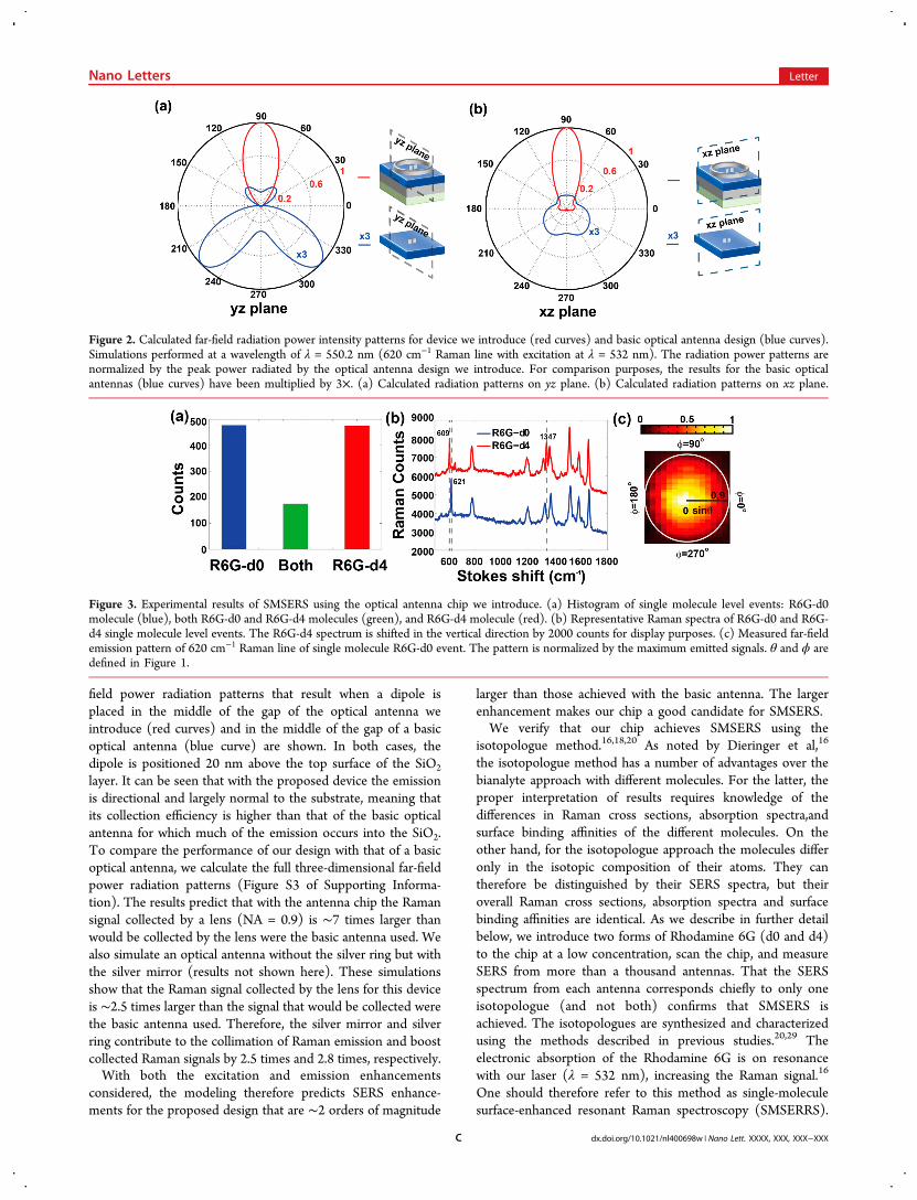
field power radiation patterns that result when a dipole isplaced in the middle of the gap of the optical antenna weintroduce (red curves) and in the middle of the gap of a basicoptical antenna (blue curve) are shown. In both cases, thedipole is positioned 20 nm above the top surface of the SiO2
layer. It can be seen that with the proposed device the emissionis directional and largely normal to the substrate, meaning thatits collection efficiency is higher than that of the basic opticalantenna for which much of the emission occurs into the SiO2.To compare the performance of our design with that of a basicoptical antenna, we calculate the full three-dimensional far-fieldpower radiation patterns (Figure S3 of Supporting Informa-tion). The results predict that with the antenna chip the Ramansignal collected by a lens (NA = 0.9) is ∼7 times larger thanwould be collected by the lens were the basic antenna used. Wealso simulate an optical antenna without the silver ring but withthe silver mirror (results not shown here). These simulationsshow that the Raman signal collected by the lens for this deviceis ∼2.5 times larger than the signal that would be collected werethe basic antenna used. Therefore, the silver mirror and silverring contribute to the collimation of Raman emission and boostcollected Raman signals by 2.5 times and 2.8 times, respectively.With both the excitation and emission enhancements
considered, the modeling therefore predicts SERS enhance-ments for the proposed design that are ∼2 orders of magnitude
larger than those achieved with the basic antenna. The largerenhancement makes our chip a good candidate for SMSERS.We verify that our chip achieves SMSERS using the
isotopologue method.16,18,20 As noted by Dieringer et al,16
the isotopologue method has a number of advantages over thebianalyte approach with different molecules. For the latter, theproper interpretation of results requires knowledge of thedifferences in Raman cross sections, absorption spectra,andsurface binding affinities of the different molecules. On theother hand, for the isotopologue approach the molecules differonly in the isotopic composition of their atoms. They cantherefore be distinguished by their SERS spectra, but theiroverall Raman cross sections, absorption spectra and surfacebinding affinities are identical. As we describe in further detailbelow, we introduce two forms of Rhodamine 6G (d0 and d4)to the chip at a low concentration, scan the chip, and measureSERS from more than a thousand antennas. That the SERSspectrum from each antenna corresponds chiefly to only oneisotopologue (and not both) confirms that SMSERS isachieved. The isotopologues are synthesized and characterizedusing the methods described in previous studies.20,29 Theelectronic absorption of the Rhodamine 6G is on resonancewith our laser (λ = 532 nm), increasing the Raman signal.16
One should therefore refer to this method as single-moleculesurface-enhanced resonant Raman spectroscopy (SMSERRS).
Figure 2. Calculated far-field radiation power intensity patterns for device we introduce (red curves) and basic optical antenna design (blue curves).Simulations performed at a wavelength of λ = 550.2 nm (620 cm−1 Raman line with excitation at λ = 532 nm). The radiation power patterns arenormalized by the peak power radiated by the optical antenna design we introduce. For comparison purposes, the results for the basic opticalantennas (blue curves) have been multiplied by 3×. (a) Calculated radiation patterns on yz plane. (b) Calculated radiation patterns on xz plane.
Figure 3. Experimental results of SMSERS using the optical antenna chip we introduce. (a) Histogram of single molecule level events: R6G-d0molecule (blue), both R6G-d0 and R6G-d4 molecules (green), and R6G-d4 molecule (red). (b) Representative Raman spectra of R6G-d0 and R6G-d4 single molecule level events. The R6G-d4 spectrum is shifted in the vertical direction by 2000 counts for display purposes. (c) Measured far-fieldemission pattern of 620 cm−1 Raman line of single molecule R6G-d0 event. The pattern is normalized by the maximum emitted signals. θ and ϕ aredefined in Figure 1.
Nano Letters Letter
dx.doi.org/10.1021/nl400698w | Nano Lett. XXXX, XXX, XXX−XXXC

For brevity, however, we follow the convention of ref 16 andrefer to it as SMSERS.The confirmation of SMSERS makes use of the fact that the
isotopologues can be readily distinguished by the Raman linethat appears at 620 and 610 cm−1 for R6G-d0 and R6G-d4,respectively. The fabricated optical antenna chip is soaked in asolution containing the isotopologues (0.2 nM each) for 12 h,washed in methanol, then blown dry with nitrogen. The opticalantenna chip is then scanned in a Raman microscope (HoribaJobin Yvon, LabRam) with a step size of 1 μm. In themicroscope, a laser beam (λ = 532 nm) is focused onto the chipwith a microscope objective (magnification 100×, numericalaperture NA 0.9). The laser power incident on the chip is 0.03mW. The same objective lens is used to collect the Ramansignal into a spectrometer equipped with a thermoelectricallycooled charge coupled device (CCD) sensor. The integrationtime used to acquire the Raman spectrum at each scan positionis 0.5 s. An 80 × 80 μm region of the chip containing 1681optical antennas is scanned. A SERS spectrum is measured ateach scan position. Among the data obtained, 1120 antennasyield strong Raman signals for the 620 and/or 610 cm−1 Ramanlines. These 1120 events can therefore be divided into threecategories: the spectrum is that of R6G-d0, the spectrum is thatof R6G-d4, and the spectrum contains both R6G-d0 and R6G-d4 features. In Figure 3a, these events are tabulated in ahistogram. It can be seen that a significant number of events(945 out of 1120 (84%)) demonstrate Raman spectracontaining either R6G-d0 or R6G-d4 but not both. ThePoisson-binomial model of the SMSERS process16 (SupportingInformation) predicts that 1120 (of the 1681) antennas wouldhave one of more molecules in their hot spots and thereforewould produce SERS signals if there were on average 1.097molecules per hot spot. The measured relative frequencies ofthe R6G-d0-only, mixed, and R6G-d4-only events are475:175:470, that is, a ratio of ∼2.7:1:2.7. This confirms thatour device achieves SMSERS. Using the Poisson-binomialmodel, and following the assumption of ref 16 that thecompetition between multiple molecules for the hot spots leadsto there being two or fewer molecules per hot spot, a ratio of∼2.3:1:2.3 would result were there on average 1.097 moleculesper hot spot. This is discussed further in the SupportingInformation. That the modeled values are close to theexperimental values confirms the very high, that is, nearunity, fraction of the optical antennas with SMSERS sensitivity.Differences between the modeled and experimental resultscould be due to the competition between multiple moleculesfor the hot spots being even more pronounced than thatassumed above, further skewing the distribution and making itdeviate from Poisson-binomial behavior. In Figure 3b,representative Raman spectra are shown for R6G-d0 andR6G-d4 single molecule events. The Raman peaks in Figure 3bshift slightly from their average values measured from largenumbers of molecules. Such peak shifts have also beenobserved in previous SMSERS studies.16,18 They representfurther confirmation that SMSERS is achieved. In theSupporting Information, the Raman intensities of R6G-d0and R6G-d4 events are shown in a histogram (Figure S4,Supporting Information). The variation in Raman signalintensity is likely to be because the molecules adsorb to thechip at random locations and therefore experience verydifferent values of local field enhancement.A central question in the field of nano-optics is whether an
antenna can be used to modify the angular distribution of light
from a single quantum emitter.30 Here we show directionalemission of Raman from single molecules. We build a systemthat enables the angular distribution of emission of each Ramanline to be measured at the back-focal-plane of the microscopeobjective (Figure S4a of Supporting Information). We fabricatean optical antenna chip and soak it in the R6G-d0/R6G-d4isotopologue solution (0.5 nM of each). The SEM image offabricated chip (not shown here) reveals that the opticalantennas have gap widths of 15 nm, slightly larger than those ofthe antennas used in the experiments of Figure 3. Simulationsof the far-field radiation pattern of the antennas with 15 nm gapare found to be very similar to those with 5 nm gaps (Figure 2)however. The measured ratio of 2.3:1:2.3 for R6G-d0-only,mixed, and R6G-d4-only confirms that the SMSERS regime isachieved. In Figure 3c, we show the measured emission patternof the 620 cm−1 Raman line, which corresponds to a R6G-d0single molecule event. It can be seen that the single moleculeemission is highly directional and occurs in a narrow range ofangles about the +z direction. The emission pattern has full-widths-at-half-maximum (fwhms) of 41 and 49° in the xz andyz planes, respectively. These represent substantial direction-ality and are close to the predicted values of 40 and 48° for thexz and yz planes, respectively (Figure 2). By comparison, thepower radiated by a dipole in free space, oriented in the x-direction, has a cos2 θ dependence. Such a dipole wouldtherefore have fwhms of 90 and 360° in the xz and yz planes,respectively. The emission pattern of an R6G-d4 singlemolecule event is also measured and shows similar propertiesto that of R6G-d0 (Figure S4c of the Supporting Information).The experimental results demonstrate the dramatic modifica-tion to the direction of Raman emission from single moleculesthat occurs when they are placed in the feed gaps of opticalantennas surrounded by silver nano rings and above a mirror.In conclusion, we experimentally demonstrate an optical
antenna chip that achieves directional SMSERS. SMSERS isone of the few methods of obtaining the vibrational spectrum ofa single molecule and presents opportunities for understandingchemical and biological systems at a fundamental level. Indeed,it is speculated that it may one day enable the observation of asingle molecule undergoing a chemical reaction.31 Weanticipate that will be very beneficial for such fundamentalscientific studies but also in technological applications. Inaddition, we foresee wider applications of antenna approachesto other types of single emitters used in quantum optics andsensing.
■ ASSOCIATED CONTENT*S Supporting InformationAdditional information and figures. This material is availablefree of charge via the Internet at http://pubs.acs.org.
■ AUTHOR INFORMATIONCorresponding Author*E-mail: [email protected] ContributionsD.W., W.Z, J.P.C., and K.B.C. developed the concept. D.W.performed fabrication and simulations. D.W. and W.Z.performed experiments and data analysis. J.P.C. and M.D.B.produced and characterized the isotopologues. D.W. and K.B.Cwrote the manuscript.NotesThe authors declare no competing financial interest.
Nano Letters Letter
dx.doi.org/10.1021/nl400698w | Nano Lett. XXXX, XXX, XXX−XXXD

■ ACKNOWLEDGMENTS
This work was supported by the National Science Foundation(NSF, grant ECCS-0747560 and grant ECCS-1201687), theHarvard Quantum Optics Center, and by the Center forExcitonics, an Energy Frontier Research Center funded by theU.S. Department of Energy, Office of Science and Office ofBasic Energy Sciences under Award Number DE-SC0001088.This work was also supported by the UT/ORNL Joint Institutefor Advanced Materials, and the U.S. Department of Energy,Office of Basic Energy Sciences, under Award Number DE-SC0004792 (J.P.C.) and the National Science Foundationunder Awards CHE-0954297 and DMR-0906752 (M.D.B.).Fabrication work was carried out in the Harvard Center forNanoscale Systems, which is supported by the NSF.
■ REFERENCES(1) Moerner, W. E. Proc. Natl. Acad. Sci. U.S.A. 2007, 104, 12596−602.(2) Mizuochi, N.; Makino, T.; Kato, H.; Takeuchi, D.; Ogura, M.;Okushi, H.; Nothaft, M.; Neumann, P.; Gali, A.; Jelezko, F.;Wrachtrup, J.; Yamasaki, S. Nat. Photonics 2012, 6, 299−303.(3) Grober, R. D.; Schoelkopf, R. J.; Prober, D. E. Appl. Phys. Lett.1997, 70, 1354−1356.(4) Crozier, K. B.; Sundaramurthy, A.; Kino, G. S.; Quate, C. F. J.Appl. Phys. 2003, 94, 4632−4642.(5) Novotny, L.; Van Hulst, N. Nat. Photonics 2011, 5, 83−90.(6) Curto, A. G.; Volpe, G.; Taminiau, T. H.; Kreuzer, M. P.;Quidant, R.; Van Hulst, N. F. Science (New York) 2010, 329, 930−3.(7) Kinkhabwala, A.; Yu, Z.; Fan, S.; Avlasevich, Y.; Mullen, K.;Moerner, W. E. Nat. Photonics 2009, 3, 654−657.(8) Lee, K. G.; Chen, X. W.; Eghlidi, H.; Kukura, P.; Lettow, R.;Renn, A.; Sandoghdar, V.; Go, S. Nat. Photonics 2011, 5, 166−169.(9) Wustholz, K. L.; Brosseau, C. L.; Casadiob, F.; Van Duyne, R. P.Phys. Chem. Chem. Phys. 2009, 11, 7350−59.(10) Fleischmann, M.; Hendra, P. J.; McQuillan, A. J. Chem. Phys.Lett. 1974, 26, 163−6.(11) Jeanmaire, D. L.; Duyne, R. P. V. A. N. J. Electroanal. Chem.Interfacial Electrochem. 1977, 84, 1−20.(12) Albrecht, M. G.; Creighton, J. A. J. Am. Chem. Soc. 1976, 99,5215−5217.(13) Nie, S.; Emory, S. R. Science 1997, 275, 1102−1106.(14) Kneipp, K.; Wang, Y.; Kneipp, H.; Perelman, L.; Itzkan, I.;Dasari, R.; Feld, M. Phys. Rev. Lett. 1997, 78, 1667−1670.(15) Ahmed, A.; Gordon, R. Nano Lett. 2012, 12, 2625−30.(16) Dieringer, J. a; Lettan, R. B.; Scheidt, K. a; Van Duyne, R. P. J.Am. Chem. Soc. 2007, 129, 16249−56.(17) Le Ru, E. C.; Grand, J.; Sow, I.; Somerville, W. R. C.; Etchegoin,P. G.; Treguer-Delapierre, M.; Charron, G.; Felidj, N.; Levi, G.;Aubard, J. Nano Lett. 2011, 11, 5013−9.(18) Kleinman, S. L.; Ringe, E.; Valleyqq, N.; Wustholz, K. L.;Phillips, E.; Scheidt, K. a; Schatz, G. C.; Van Duyne, R. P. J. Am. Chem.Soc. 2011, 133, 4115−22.(19) Blackie, E. J.; Le Ru, E. C.; Etchegoin, P. G. J. Am. Chem. Soc.2009, 131, 14466−72.(20) Blackie, E.; Le Ru, E. C.; Meyer, M.; Timmer, M.; Burkett, B.;Northcote, P.; Etchegoin, P. G. Phys. Chem. Chem. Phys. 2008, 10,4147−53.(21) Etchegoin, P. G.; Meyer, M.; Blackie, E.; Le Ru, E. C. Anal.Chem. 2007, 79, 8411−5.(22) Le Ru, E. C.; Meyer, M.; Etchegoin, P. G. J. Phys. Chem. B 2006,110, 1944−8.(23) Camden, J. P.; Dieringer, J. a; Wang, Y.; Masiello, D. J.; Marks,L. D.; Schatz, G. C.; Van Duyne, R. P. J. Am. Chem. Soc. 2008, 130,12616−7.(24) Zhu, W.; Banaee, M. G.; Wang, D.; Chu, Y.; Crozier, K. B. Small2011, 7, 1761−6.
(25) Chu, Y.; Banaee, M. G.; Crozier, K. B. ACS Nano 2010, 4,2804−2810.(26) Seok, T. J.; Jamshidi, A.; Kim, M.; Dhuey, S.; Lakhani, A.; Choo,H.; Schuck, P. J.; Cabrini, S.; Schwartzberg, A. M.; Bokor, J.;Yablonovitch, E.; Wu, M. C. Nano Lett. 2011, 11, 2606−10.(27) Wang, D.; Yang, T.; Crozier, K. B. Opt. Express 2011, 19, 2148−57.(28) Ahmed, A.; Gordon, R. Nano Lett. 2011, 11, 1800−3.(29) Mirsaleh-kohan, N.; Iberi, V.; Simmons, P. D.; Bigelow, N. W.;Vaschillo, A.; Rowland, M. M.; Best, M. D.; Pennycook, S. J.; Masiello,D. J.; Guiton, B. S.; Camden, J. P. J. Chem. Phys. Lett. 2012, 3, 2303−2309.(30) Greffet, J.-J. Science (New York) 2005, 308, 1561−3.(31) Sharma, B.; Frontiera, R. R.; Henry, A.-I.; Ringe, E.; Van Duyne,R. P. Mater. Today 2012, 15, 16−25.
Nano Letters Letter
dx.doi.org/10.1021/nl400698w | Nano Lett. XXXX, XXX, XXX−XXXE