direct time-resolved observation of tungsten...
TRANSCRIPT

This content has been downloaded from IOPscience. Please scroll down to see the full text.
Download details:
IP Address: 128.174.163.172
This content was downloaded on 14/03/2015 at 17:31
Please note that terms and conditions apply.
Direct time-resolved observation of tungsten nanostructured growth due to helium plasma
exposure
View the table of contents for this issue, or go to the journal homepage for more
2015 Nucl. Fusion 55 033020
(http://iopscience.iop.org/0029-5515/55/3/033020)
Home Search Collections Journals About Contact us My IOPscience

| International Atomic Energy Agency Nuclear Fusion
Nucl. Fusion 55 (2015) 033020 (7pp) doi:10.1088/0029-5515/55/3/033020
Direct time-resolved observation oftungsten nanostructured growth due tohelium plasma exposure
P. Fiflis, D. Curreli and D.N. Ruzic
Center for Plasma Material Interactions, Department of Nuclear, Plasma and RadiologicalEngineering, University Illinois at Urbana-Champaign, Urbana, IL 61801, USA
E-mail: [email protected]
Received 9 October 2014, revised 11 December 2014Accepted for publication 12 February 2015Published 4 March 2015
AbstractDetermination of the mechanisms underlying the growth of tungsten fuzz is an important step towards mitigation of fuzzformation. Nanostructured tungsten was produced on resistively heated tungsten wires in a helicon plasma source (maximumflux of 2.5 × 10²¹ m−2 s−1). Asymmetry in the setup allows for investigation of temperature and flux effects in a single sample.An effort at elucidating the mechanism of formation was made by inspecting SEM micrographs of the nanostructured tungstenat successive fluence steps of helium ions up to a fluence of 1 × 1027 m−2. To create these micrographs a single tungstensample was exposed to the plasma, removed and inspected with an SEM, and replaced into the plasma. The tungsten surfacewas marked in several locations so that each micrograph is centred within 200 nm of each previous micrograph. Pitting of thesurface (diameter 9.5 ± 2.3 nm, fluence (5 ± 2)×1025 m−2) followed by surface roughening (fluence (9 ± 2) × 1025 m−2) andtendril formation (diameter 30 ± 10 nm, fluence (2 ± 1) × 1026 m−2) is observed, providing evidence of bubble bursting as themechanism for seeding the growth of the tungsten fuzz.
Keywords: tungsten fuzz, divertor material, bubbles and blisters
(Some figures may appear in colour only in the online journal)
Under irradiation by helium plasmas, tungsten surfaces atelevated temperatures have shown evidence of nanostructur-ing [1]. At temperatures between 1000 and 2000 K, and atfluxes in excess of 2×10²⁰ m−2 s−1, this nanostructuring takesthe form of nanotendrils colloquially referred to as ‘tungstenfuzz’ [2]. The tungsten surfaces in the International Thermonu-clear Experimental Reactor (ITER) will be exposed to largehelium fluxes at high temperature [3, 4]. This has promptedfurther investigation into the formation of tungsten fuzz in toka-maks. Studies have demonstrated fuzz formation in fusion de-vices [2]. Traditionally, tungsten fuzz has been produced inlinear plasma devices capable of delivering large fluxes at ele-vated temperatures [5–7]. However, a recent study has demon-strated fuzz formation in a smaller test stand under exposurefrom a helicon plasma [8]. To date, most of these experimentsexpose a single sample to a single flux at a single temperature,and therefore studies can only show fluence/flux steps at a settemperature. A unique geometry employed at the Universityof Illinois allows for the exposure of a single sample of tung-sten wire wound around an alumina tube to a helicon plasma.Due to the geometry, the wire is exposed to a variety of fluxesand a range of temperatures.
The experimental setup consists of a MORI 200 heliconplasma source [9] and a resistively heated tungsten wire
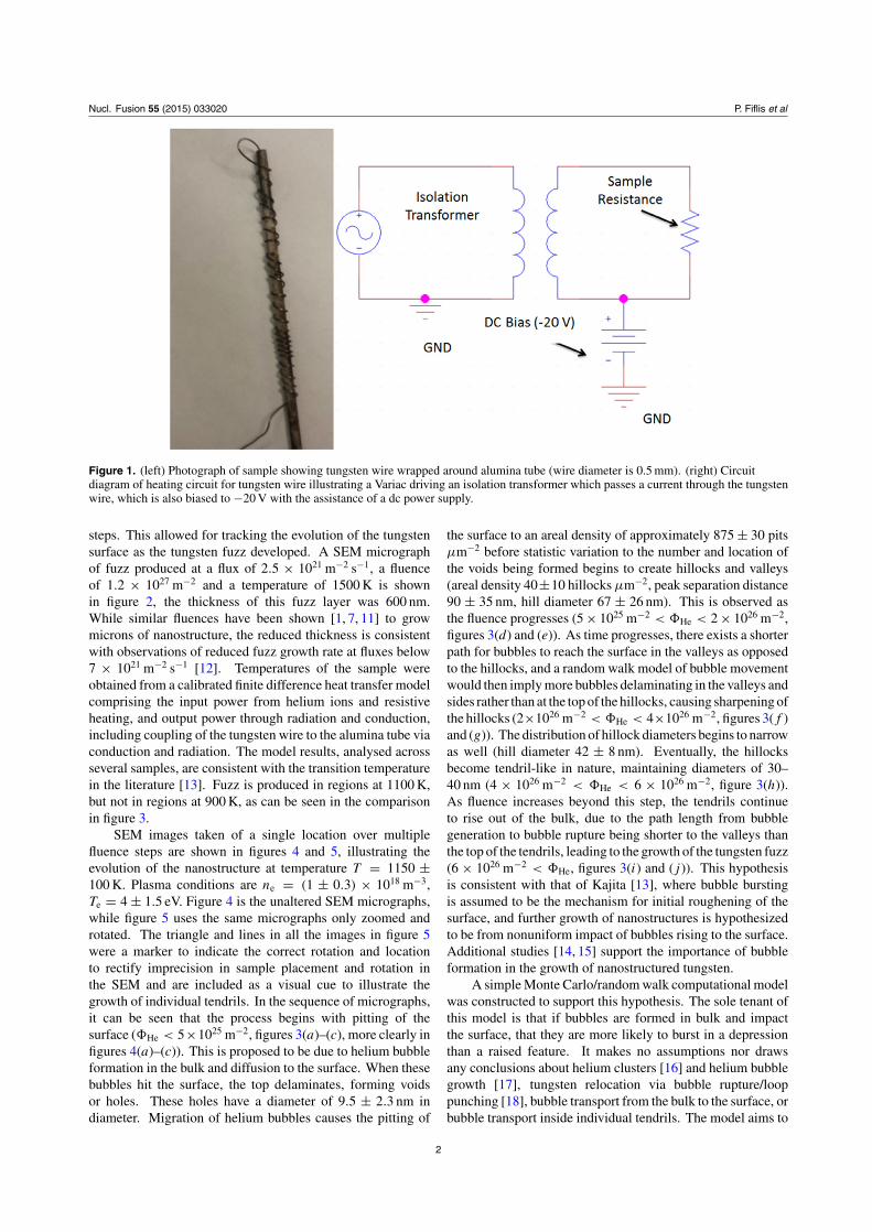
mounted on an alumina tube. The helicon plasma for theexposures detailed herein was run at an RF power of 700 W,a helium pressure of 100 mTorr, and a magnetic field of120 G. RF compensated Langmuir probe measurements ofthe plasma return a density of (1.0 ± 0.3) × 1018 m−3 anda temperature of 4 ± 1.5 eV in the region where the samplewas placed [10]. The sample consists of a 0.5 mm diametertungsten wire (extruded, annealed, 99.95%, Alfa Aesar). Thesample is passed through and then wound around an aluminatube. A photo of the wire and a circuit diagram are shown infigure 1.To achieve temperatures necessary for fuzz formationa current was passed through the wire to heat it. Thisconfiguration was chosen so that the tungsten surface exposedto the plasma would have a broad temperature profile. Thewire was then biased to a negative voltage with respected toplasma potential. In this case, the wire was biased at 40 Vbelow plasma potential resulting in 40 eV helium ions at aflux of 2.5 × 10²¹ m−2 s−1 which is well within the range ofions used for the production of nanostructured tungsten onlinear plasma devices [11]. Scanning electron microscopy(Hitachi S-4700) is performed on the samples after exposureto the helium plasma. The tungsten wire was indented inmultiple locations with a diamond bandsaw to recover imagesof the same location on an SEM tool in between fluence
0029-5515/15/033020+07$33.00 1 © 2015 IAEA, Vienna Printed in the UK
Nucl. Fusion 55 (2015) 033020 P. Fiflis et al
Figure 1. (left) Photograph of sample showing tungsten wire wrapped around alumina tube (wire diameter is 0.5 mm). (right) Circuitdiagram of heating circuit for tungsten wire illustrating a Variac driving an isolation transformer which passes a current through the tungstenwire, which is also biased to −20 V with the assistance of a dc power supply.
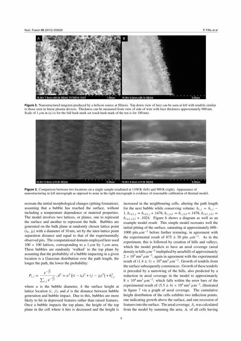
steps. This allowed for tracking the evolution of the tungstensurface as the tungsten fuzz developed. A SEM micrographof fuzz produced at a flux of 2.5 × 10²¹ m−2 s−1, a fluenceof 1.2 × 1027 m−2 and a temperature of 1500 K is shownin figure 2, the thickness of this fuzz layer was 600 nm.While similar fluences have been shown [1, 7, 11] to growmicrons of nanostructure, the reduced thickness is consistentwith observations of reduced fuzz growth rate at fluxes below7 × 1021 m−2 s−1 [12]. Temperatures of the sample wereobtained from a calibrated finite difference heat transfer modelcomprising the input power from helium ions and resistiveheating, and output power through radiation and conduction,including coupling of the tungsten wire to the alumina tube viaconduction and radiation. The model results, analysed acrossseveral samples, are consistent with the transition temperaturein the literature [13]. Fuzz is produced in regions at 1100 K,but not in regions at 900 K, as can be seen in the comparisonin figure 3.
SEM images taken of a single location over multiplefluence steps are shown in figures 4 and 5, illustrating theevolution of the nanostructure at temperature T = 1150 ±100 K. Plasma conditions are ne = (1 ± 0.3) × 1018 m−3,Te = 4 ± 1.5 eV. Figure 4 is the unaltered SEM micrographs,while figure 5 uses the same micrographs only zoomed androtated. The triangle and lines in all the images in figure 5were a marker to indicate the correct rotation and locationto rectify imprecision in sample placement and rotation inthe SEM and are included as a visual cue to illustrate thegrowth of individual tendrils. In the sequence of micrographs,it can be seen that the process begins with pitting of thesurface (�He < 5×1025 m−2, figures 3(a)–(c), more clearly infigures 4(a)–(c)). This is proposed to be due to helium bubbleformation in the bulk and diffusion to the surface. When thesebubbles hit the surface, the top delaminates, forming voidsor holes. These holes have a diameter of 9.5 ± 2.3 nm indiameter. Migration of helium bubbles causes the pitting of
the surface to an areal density of approximately 875 ± 30 pitsµm−2 before statistic variation to the number and location ofthe voids being formed begins to create hillocks and valleys(areal density 40±10 hillocks µm−2, peak separation distance90 ± 35 nm, hill diameter 67 ± 26 nm). This is observed asthe fluence progresses (5 × 1025 m−2 < �He < 2 × 1026 m−2,figures 3(d) and (e)). As time progresses, there exists a shorterpath for bubbles to reach the surface in the valleys as opposedto the hillocks, and a random walk model of bubble movementwould then imply more bubbles delaminating in the valleys andsides rather than at the top of the hillocks, causing sharpening ofthe hillocks (2×1026 m−2 < �He < 4×1026 m−2, figures 3(f )and (g)). The distribution of hillock diameters begins to narrowas well (hill diameter 42 ± 8 nm). Eventually, the hillocksbecome tendril-like in nature, maintaining diameters of 30–40 nm (4 × 1026 m−2 < �He < 6 × 1026 m−2, figure 3(h)).As fluence increases beyond this step, the tendrils continueto rise out of the bulk, due to the path length from bubblegeneration to bubble rupture being shorter to the valleys thanthe top of the tendrils, leading to the growth of the tungsten fuzz(6 × 1026 m−2 < �He, figures 3(i) and (j )). This hypothesisis consistent with that of Kajita [13], where bubble burstingis assumed to be the mechanism for initial roughening of thesurface, and further growth of nanostructures is hypothesizedto be from nonuniform impact of bubbles rising to the surface.Additional studies [14, 15] support the importance of bubbleformation in the growth of nanostructured tungsten.
A simple Monte Carlo/random walk computational modelwas constructed to support this hypothesis. The sole tenant ofthis model is that if bubbles are formed in bulk and impactthe surface, that they are more likely to burst in a depressionthan a raised feature. It makes no assumptions nor drawsany conclusions about helium clusters [16] and helium bubblegrowth [17], tungsten relocation via bubble rupture/looppunching [18], bubble transport from the bulk to the surface, orbubble transport inside individual tendrils. The model aims to
2
Nucl. Fusion 55 (2015) 033020 P. Fiflis et al
Figure 2. Nanostructured tungsten produced by a helicon source at Illinois. Top down view of fuzz can be seen at left with tendrils similarto those seen in linear plasma devices. Thickness can be measured from view of side of wire with fuzz thickness approximately 600 nm.Scale of 1 µm in (a) is for the full hash mark set (each hash mark of the ten is for 100 nm).
Figure 3. Comparison between two locations on a single sample irradiated at 1100 K (left) and 900 K (right). Appearance ofnanostructuring in left micrograph as opposed to none in the right micrograph is evidence of reasonable calibration of thermal model.
recreate the initial morphological changes (pitting formation),assuming that a bubble has reached the surface, withoutincluding a temperature dependence or material properties.The model involves two lattices, or planes, one to representthe surface and another to represent the bulk. Bubbles aregenerated on the bulk plane at randomly chosen lattice point(i0, j0) with a diameter of 10 nm, set by the inter-lattice pointseparation distance and equal to that of the experimentallyobserved pits. The computational domain employed here used100 × 100 lattices, corresponding to a 1 µm by 1 µm area.These bubbles are randomly ‘walked’ to the top plane byassuming that the probability of a bubble impacting in a givenlocation is a Gaussian distribution over the path length, thelonger the path, the lower the probability:
Pi,j = e− d2
σ2
∑i,j e− d2
σ2
, d2 = a2((i − i0)
2 + (j − j0)2)
+ h2i,j
where a is the bubble diameter, h the surface height atlattice location (i, j), and d is the distance between bubblegeneration and bubble impact. Due to this, bubbles are morelikely to hit in depressed features rather than raised features.Once a bubble impacts the top plane, the height of the topplane in the cell where it hits is decreased and the height is
increased in the neighbouring cells, altering the path lengthfor the next bubble while conserving volume: hi,j = hi,j −1, hi±1,j = hi±1,j + .1476, hi,j±1 = hi,j±1 + .1476, hi±1,j±1 =hi±1,j±1 + .1024. Figure 6 shows a diagram as well as anexample model result. This simple model recreates well theinitial pitting of the surface, saturating at approximately 600–1000 pits µm−2 before further texturing, in agreement withthe experimental result of 875 ± 30 pits µm−2. As in theexperiment, this is followed by creation of hills and valleys,which the model predicts to have an areal coverage (arealdensity in hills µm−2 multiplied by area/hill) of approximately2 × 105 nm2 µm−2, again in agreement with the experimentalresult of (1.4 ± 1) × 105 nm2 µm−2. Growth of tendrils fromthe surface subsequently commences. Growth of these tendrilsis preceded by a narrowing of the hills, also predicted by areduction in areal coverage in the model to approximately8 × 104 nm2 µm−2, which falls within the error bars of theexperimental result of (5.5 ± 4) × 104 nm2 µm−2, illustratedin figure 7 via a graph of areal coverage. The cumulativeheight distribution of the cells exhibits two inflection points,one indicating growth above the surface, and one recession offeatures into the surface. The areal coverage, Ac was calculatedfrom the model by summing the area, Ai of all cells having
3

Nucl. Fusion 55 (2015) 033020 P. Fiflis et al
Figure 4. Temporal (and therefore fluence) evolution ofnanostructures at 1150 K. (a)–(c) show the appearance of pits in thesurface (more evident in figure 5). (d) and (e) show continuedroughening of the surface leading to the onset of hill and valleyformation. (f ) and (g) illustrate continued ‘pitting’ of the surfacefrom bubble rupture, which we hypothesize leads to narrowing ofthe hills. In (h)–(j ) the narrowed hills continue to grow from thesurface as the onset of fuzz formation.
height hi above a critical height, hcrit . Ac = ∑i Ai where
Ai
{Ai �= 0 if hi > hcrit
Ai = 0 if hi < hcrit
where hcrit is determined by the upper inflection point in thecumulative height distribution:
d
dH 2
∑
j
H∑−∞
hj<H
∣∣∣∣∣∣H=hcrit
= 0.
The critical height, hcrit , varies with fluence and is a clearindicator of what has grown out of the surface and what has not.Assuming the bubble formation rate to be linearly proportional
Figure 5. Zoomed, rotated and aligned micrographs of figure 3.Green lines used as both visual cue and method of alignment.Evolution and growth of individual tendrils of approximately30–40 nm in diameter is evident.
to helium fluence at small thicknesses of fuzz, and setting 1000bubbles equal to a fluence of 5 × 1025 m−2 (pitting saturationoccurring at <1000 bubbles in the model and approximately5 × 1025 m−2 experimentally), the model predicts hill growthbetween fluences of 1.5×1026 to 4×1026 m−2. It then predictshill sharpening and eventual fuzz growth at fluences greaterthan 4 × 1026 m−2, similar to those measured experimentally.Finally, a measurement of the radial distribution function of thetendrils from the model suggests an inter-tendril separationof 50–60 nm which roughly agrees with the experimentallyobtained inter-tendril separation of 90 ± 35 nm. Table 1 is asummary of these comparisons. A series of plots of the surfaceheight over time from the model is shown in figure 8 such thatit complements the progression of figure 5.
1. Discussion and summary
The experimental results detailed here mark for the firsttime, to the knowledge of the authors, the observation ofindividual nanostructured tendrils at progressive fluence levels
4

Nucl. Fusion 55 (2015) 033020 P. Fiflis et al
Figure 6. (left) Schematic of fuzz growth model showing bubble generation in plane A (bulk plane), impact in plane B (surface plane) andmodification of the surface height (blue arrow illustrating decrement and red arrows incrementing of adjacent cells). (right) Side view ofmodel nano-‘fuzz’, in units of 10 nm at simulation end (beginning of tendril growth phase). Tendril growth and bulk recession can be readilyobserved.
Figure 7. Areal coverage of nanostructure features versus bubble count. Curve progresses through initial pitting of the surface to a bubblecount of 600–1000 bubbles per square micron (highlighted in green) before further nanostructuring of the surface. Hillock growth(highlighted in red) follows reaching a maximum areal coverage of about 2 × 10⁵ nm2 µm−2 before gradually thinning into nanostructuredtendrils (highlighted in orange).
Table 1. Comparison of morphological data from experiment and model. The only free parameter of impact in the model is that 1000He bubbles result from a fluence of 5 × 1025 He+ m−2.
Experimental Model Experimental Model fluence (scaled toobservation analogue fluence match pitting threshold)
Pitting of surface saturates at Pitting of surface saturates between 5 × 1025 m−2 He+ ions 5 × 1025 m−2 He+ ions875 ± 30 pits µm−2 600 and 1000 pits µm−2
Hill areal coverage Hill areal coverage 5 × 1025–2 × 1026 m−2 1.5 × 1026–4.5 × 1026 m−2
(1.4 ± 1) × 105 nm2 µm−2 2 × 10⁵ nm2 µm−2 He+ ions He+ ionsTendril thinning and growth, areal Tendril thinning and growth, >2 × 1026 m−2 He+ ions > 4.5 × 1026 m−2 He+ ions
coverage (5.5 ± 4) × 104 nm2 µm−2 areal coverage 8 × 10⁴ nm2 µm−2
Inter-tendril separation 90 ± 35 nm Inter-tendril separation 50–60 nm — —
on the same sample. The series of micrographs presentedherein shows an evolution of a tungsten surface that firstshows evidence of pitting at low fluences, followed by furtherdeformation into a series of hills and valleys that progress toform the tungsten nanotendrils. The experimental findings
support the theory of Kajita et al [13], as well as provide abenchmark that may be used for validation of morphologiespredicted by computational codes.
The much simpler computational model employed hereserves to test the hypothesis detailed at the end of the
5

Nucl. Fusion 55 (2015) 033020 P. Fiflis et al
Figure 8. Computational model results presented as analogue ofmicrographs in figure 4. Again, a triangle (white), is used as a visualcue to show evolution of individual nanostructures. Similarqualitative phenomena can be seen, with pitting of the originalsurface (light blue (a)–(c)), hill and valley formation (yellow/blue(d)–(g)), hill sharpening (orange/red (h)) and finally, nanotendrilgrowth (red (i)–(j )). Each cell dimension is 10 × 10 nm (initial pitradius ∼10 nm). The colour scale at bottom also in units of 10 nm.
experimental section. By modelling only the simpleassumption that a bubble created in the bulk is more likelyto impact in a depressed feature, rather than a raised feature,the pitting density saturation, hill formation and narrowinginto tendrils, as well as the areal feature coverage are matchedbetween experiment and model.
Additionally, assuming that the number of bubblesproduced is linearly proportional to the fluence at small fuzzthickness results in similar numbers for the fluences at whichhills are formed and thin into tendrils when equating 1000bubbles to a fluence of 5 × 1025 m−2 (pitting saturation). If allof the helium incident on the sample were in the 10 nm bubbles,this would lead to pressures much higher than the 10s of Gbar
predicted by MD simulations [14]. This discrepancy could beaccounted for by annealing of the surface leading to a highernumber of bubbles required to create the same morphologicalchanges, or the presence of helium sinks in the material thatdo not lead to bubble formation (i.e. grain boundaries [19], orhelium atom diffusion to the surface).
Finally, it should also be noted here that the hypothesispresented here as well as the model supporting that hypothesisonly account for the initial morphological changes. As the fuzzlayer continues to grow to thicknesses much greater than thefuzz tendril diameter, ion implantation should occur primarilyin the tendrils rather than the bulk; a complication also alludedto by Kajita [13]. Further growth, however, may be explainedby the surface diffusion model proposed by Martynenko [20],and supported by Miyamoto [15].
References
[1] Baldwin M.J. and Doerner R.P. 2010 Formation of heliuminduced nanostructure ‘fuzz’ on various tungsten grainsJ. Nucl. Mater. 404 165–73
[2] Wright G.M. et al 2013 Comparison of tungsten nano-tendrilsgrown in Alcator C-Mod and linear plasma devices J. Nucl.Mater. 438 S84–9
[3] Brooks J.N., Allain J.P., Doerner R.P., Hassanein A., NygrenR., Rognlien T.D. and Whyte D.G. 2009 Plasma–surfaceinteraction issues of an all-metal ITER Nucl. Fusion49 035007
[4] Najmabadi F. and the ARIES Team 2006 The ARIES-ATadvanced tokamak. Advanced technology fusion powerplant Fusion Eng. Des. 80 3–23
[5] Takamura S., Ohno N., Nishijima D. and Kajita S. 2006Formation of nanostructured tungsten with arborescentshape due to helium plasma irradiation Plasma Fusion Res.1 051
[6] De Temmerman G., Bystrov K., Zielinski J., Balden M.,Matern G., Arnas C. and Marot L. 2012 Nanostructuring ofmolybdenum and tungsten surfaces by low-energy heliumions J. Vac. Sci. Technol. A 30 041306
[7] Baldwin M.J. and Doerner R.P. 2008 Helium inducednanoscopic morphology on tungsten under fusion relevantplasma conditions Nucl. Fusion 48 5
[8] Baldwin M.J., Lynch T.C., Doerner R.P. and Yu J.H. 2011Nanostructure formation on tungsten exposed tolow-pressure rf helium plasmas: a study of ion energythreshold and early stage growth J. Nucl. Mater. 415 S104–7
[9] Ruzic D.N. 1994 Electric Probes for Low TemperaturePlasmas (New York: American Vacuum Society EducationCommittee)
[10] Tobe R., Sekiguchi A., Sasaki M., Okada O. and Hosokawa N.1996 Thin Solid Films 281–282 155–8
[11] Baldwin M.J., Doerner R.P., Nishijima D., Tokunaga K. andUeda Y. 2009 The effects of high fluence mixed-species(deuterium, helium, beryllium) plasma interactions withtungsten J. Nucl. Mater. 390–391 886–90
[12] Doerner R.P., Baldwin M.J. and Stangeby P.C. 2011 Anequilibrium model for tungsten fuzz in an eroding plasmaenvironment Nucl. Fusion 51 043001
[13] Kajita S., Yoshida N., Yoshihara R., Ohno N. andYamagiwa M. 2011 TEM observation of the growth processof helium nanobubbles on tungsten: nanostructureformation mechanism J. Nucl. Mater. 418 152–8
[14] De Temmerman G., Bystrov K., Doerner R.P., Marot L.,Wright G.M., Woller K.B., Whyte D.G. and Zielinski J.J.2013 Helium effects on tungsten under fusion-relevantplasma loading conditions J. Nucl. Mater. 438 S78–83
6

Nucl. Fusion 55 (2015) 033020 P. Fiflis et al
[15] Miyamoto M., Watanabe T., Nagashima H., Nishijima D.,Doerner R.P., Krasheninnikov S.I., Sagara A. andYoshida N. 2014 In situ transmission electron microscopeobservations of the formation of fuzzy structures ontungsten Phys. Scr. T159 014028
[16] Hu L., Hammond K.D., Wirth B.D. and Maroudas D. 2014Dynamics of small mobile helium clusters near tungstensurfaces Surf. Sci. 626 L21–5
[17] Sefta F., Juslin N. and Wirth B.D. 2013 Helium bubblebursting in tungsten J. Appl. Phys. 114 243518
[18] Lasa A., Tahtinen S.K. and Nordlund K. 2014 Loop punchingand bubble rupture causing surface roughening: a model forW fuzz growth Europhys. Lett. 105 25002
[19] El-Atwani O., Efe M., Heim B. and Allain J.P. 2013 Surfacedamage in ultrafine and multimodel grained tungstenmaterials induced by low energy helium irradiation J. Nucl.Mater. 434 170–7
[20] Martynenko Y.V. and Nagel M.Y. 2012 Model of fuzzformation on a tungsten surface Plasma Phys. Rep.38 996–9
7