digital system implementation - harvey mudd...
TRANSCRIPT
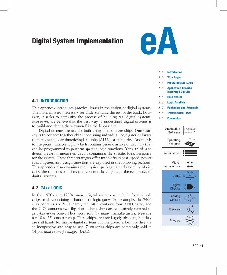
eADigital System Implementation
A.1 INTRODUCTION
This appendix introduces practical issues in the design of digital systems.The material is not necessary for understanding the rest of the book, how-ever, it seeks to demystify the process of building real digital systems.Moreover, we believe that the best way to understand digital systems isto build and debug them yourself in the laboratory.
Digital systems are usually built using one or more chips. One strat-egy is to connect together chips containing individual logic gates or largerelements such as arithmetic/logical units (ALUs) or memories. Another isto use programmable logic, which contains generic arrays of circuitry thatcan be programmed to perform specific logic functions. Yet a third is todesign a custom integrated circuit containing the specific logic necessaryfor the system. These three strategies offer trade-offs in cost, speed, powerconsumption, and design time that are explored in the following sections.This appendix also examines the physical packaging and assembly of cir-cuits, the transmission lines that connect the chips, and the economics ofdigital systems.
A.2 74xx LOGIC
In the 1970s and 1980s, many digital systems were built from simplechips, each containing a handful of logic gates. For example, the 7404chip contains six NOT gates, the 7408 contains four AND gates, andthe 7474 contains two flip-flops. These chips are collectively referred toas 74xx-series logic. They were sold by many manufacturers, typicallyfor 10 to 25 cents per chip. These chips are now largely obsolete, but theyare still handy for simple digital systems or class projects, because they areso inexpensive and easy to use. 74xx-series chips are commonly sold in14-pin dual inline packages (DIPs).
A.1 Introduction
A.2 74xx Logic
A.3 Programmable Logic
A.4 Application-SpecificIntegrated Circuits
A.5 Data Sheets
A.6 Logic Families
A.7 Packaging and Assembly
A.8 Transmission Lines
A.9 Economics
+
+−
Physics
Devices
AnalogCircuits
DigitalCircuits
Logic
Micro-architecture
Architecture
OperatingSystems
ApplicationSoftware
>”helloworld!”
533.e1

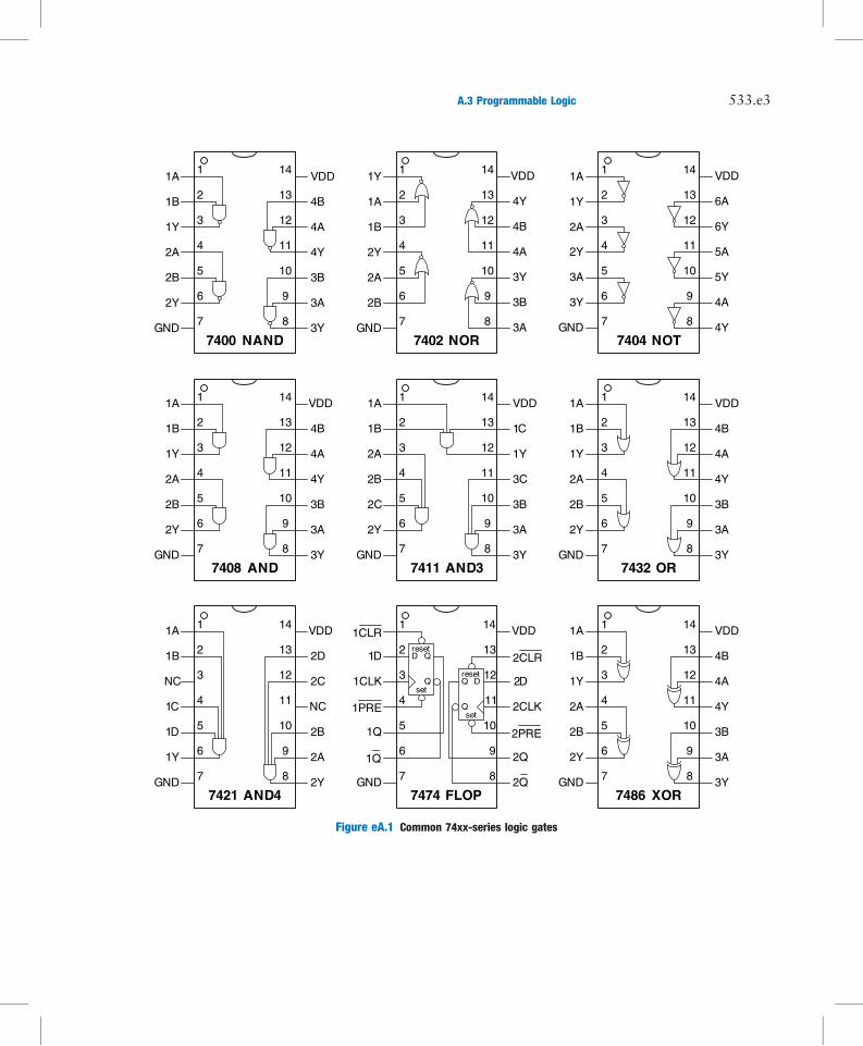
A . 2 . 1 Logic Gates
Figure eA.1 shows the pinout diagrams for a variety of popular 74xx-serieschips containing basic logic gates. These are sometimes called small-scaleintegration (SSI) chips, because they are built from a few transistors. The14-pin packages typically have a notch at the top or a dot on the top leftto indicate orientation. Pins are numbered starting with 1 in the upper leftand going counterclockwise around the package. The chips need to receivepower (VDD= 5 V) and ground (GND = 0 V) at pins 14 and 7, respectively.The number of logic gates on the chip is determined by the number of pins.Note that pins 3 and 11 of the 7421 chip are not connected (NC) to any-thing. The 7474 flip-flop has the usual D, CLK, and Q terminals. It alsohas a complementary output, Q: Moreover, it receives asynchronous set(also called preset, or PRE) and reset (also called clear, or CLR) signals.These are active low; in other words, the flop sets when PRE = 0, resetswhen CLR = 0, and operates normally when PRE = CLR = 1:
A . 2 . 2 Other Functions
The 74xx series also includes somewhat more complex logic functions,including those shown in Figures eA.2 and eA.3. These are called med-ium-scale integration (MSI) chips. Most use larger packages to accommo-date more inputs and outputs. Power and ground are still provided at theupper right and lower left, respectively, of each chip. A general functionaldescription is provided for each chip. See the manufacturer’s data sheets forcomplete descriptions.
A.3 PROGRAMMABLE LOGIC
Programmable logic consists of arrays of circuitry that can be configured toperform specific logic functions. We have already introduced three formsof programmable logic: programmable read only memories (PROMs), pro-grammable logic arrays (PLAs), and field programmable gate arrays(FPGAs). This section shows chip implementations for each of these. Con-figuration of these chips may be performed by blowing on-chip fuses toconnect or disconnect circuit elements. This is called one-time programma-ble (OTP) logic because, once a fuse is blown, it cannot be restored. Alter-natively, the configuration may be stored in a memory that can bereprogrammed at will. Reprogrammable logic is convenient in the labora-tory because the same chip can be reused during development.
A . 3 . 1 PROMs
As discussed in Section 5.5.7, PROMs can be used as lookup tables.A 2N-word ×M-bit PROM can be programmed to perform any combina-tional function of N inputs and M outputs. Design changes simply involve
74LS04 inverter chip in a 14-pindual inline package. The partnumber is on the first line. LSindicates the logic family (seeSection A.6). The N suffixindicates aDIPpackage.The largeS is the logo of the manufacturer,Signetics. The bottom two lines ofgibberish are codes indicating thebatch in which the chip wasmanufactured.
533.e2 APPENDIX A Digital System Implementation
DQ
Q
1
2
3
4
5
6
7
14
13
12
11
10
9
8GND
VDD1A
1B
1Y
2A
2B
2Y
4B
4A
4Y
3B
3A
3Y7400 NAND
1
2
3
4
5
6
7
14
13
12
11
10
9
8GND
VDD1Y
1A
1B
2Y
2A
2B
4Y
4B
4A
3Y
3B
3A7402 NOR
1
2
3
4
5
6
7
14
13
12
11
10
9
8GND
VDD1A
1Y
2A
2Y
3A
3Y
6A
6Y
5A
5Y
4A
4Y7404 NOT
1
2
3
4
5
6
7
14
13
12
11
10
9
8GND
VDD1A
1B
2A
2B
2C
2Y
1C
1Y
3C
3B
3A
3Y7411 AND3
1
2
3
4
5
6
7
14
13
12
11
10
9
8GND
VDD1A
1B
1Y
2A
2B
2Y
4B
4A
4Y
3B
3A
3Y7408 AND
1
2
3
4
5
6
7
14
13
12
11
10
9
8
VDD1A
1B
1Y
2A
2B
2Y
4B
4A
4Y
3B
3A
3Y7486 XOR
GND
1
2
3
4
5
6
7
14
13
12
11
10
9
8
VDD1A
1B
1Y
2A
2B
2Y
4B
4A
4Y
3B
3A
3Y7432 OR
GND
1
2
3
4
5
6
7
14
13
12
11
10
9
8GND
VDD1A
1B
1C
1D
1Y
2D
2C
NC
2B
2A
2Y7421 AND4
NC
1
2
3
4
5
6
7
14
13
12
11
10
9
8GND
VDD
1D
1Q
7474 FLOP
1CLK
1CLR
1PRE
1Q
2CLR
2D
2PRE
2Q
2Q
2CLK
reset
set
D Q
Qreset
set
Figure eA.1 Common 74xx-series logic gates
A.3 Programmable Logic 533.e3

CLR
CLK
D0
D1
D2
D3
ENP
GND
74161 /163 Counter
VDD
Q0
RCO
LOAD
ENT
1
2
3
4
5
6
7
8
16
15
14
13
12
11
10
9
Q1
Q2
Q3
always_ff @(posedge CLK) // 74163 if (~CLRb) Q <= 4'b0000; else if (~LOADb) Q <= D; else if (ENP & ENT) Q <= Q+1;
assign RCO = (Q == 4'b1111) & ENT;
4-bit CounterCLK: clockQ3:0: counter outputD3:0: parallel inputCLRb: async reset (161)
sync reset (163) LOADb: load Q from DENP, ENT: enablesRCO: ripple carry out
1G
S1
1D3
1D2
1D1
1D0
1Y
GND
74153 4 :1 Mux
VDD
2G
S0
2D3
2D2
2D1
2D0
2Y
1
2
3
4
5
6
7
8
16
15
14
13
12
11
10
9
always_comb if (1Gb) 1Y = 0; else 1Y = 1D[S];always_comb if (2Gb) 2Y = 0; else 2Y = 2D[S];
Two 4:1 MultiplexersD3:0: dataS1:0: selectY: outputGb: enable
A0
A1
A2
G2A
G2B
G1
Y7
GND
74138 3 :8 Decoder
VDD
Y0
Y1
Y2
Y3
Y4
Y5
Y6
1
2
3
4
5
6
7
8
16
15
14
13
12
11
10
9
3:8 DecoderA2:0: address
outputG1: active high enableG2: active low enablesG1 G2A G2B A2:0 Y7:00 x x xxx 111111111 1 x xxx 111111111 0 1 xxx 111111111 0 0
1Y
S
1D0
1D1
2D0
2D1
2Y
GND
74157 2 :1 Mux
VDD
G
4D0
4D1
4Y
3D0
3D1
3Y
1
2
3
4
5
6
7
8
16
15
14
13
12
11
10
9
always_comb if (Gb) 1Y = 0; else 1Y = S ? 1D[1] : 1D[0]; if (Gb) 2Y = 0; else 2Y = S ? 2D[1] : 2D[0]; if (Gb) 3Y = 0; else 3Y = S ? 3D[1] : 3D[0]; if (Gb) 4Y = 0; else 4Y = S ? 4D[1] : 4D[0];
Four 2:1 MultiplexersD1:0: dataS: selectY: outputGb: enable
1EN
1A0
2Y3
1A1
2Y2
GND
74244 Tristate Buffer
VDD
2EN
1Y0
2A3
1Y1
2A2
1Y2
2A1
1
2
3
4
5
6
7
8
20
19
18
17
16
15
14
13
9
10
12
11
1A2
2Y1
1A3
1Y0 1Y3
2A0
assign 1Y = 1ENb ? 4'bzzzz : 1A;assign 2Y =
2ENb ? 4'bzzzz : 2A;
8-bit Tristate BufferA3:0: inputY3:0: outputENb: enable
always_ff @(posedge CLK) if (~ENb) Q <= D;
EN
Q0
D0
D1
Q1
GND
74377 Register
VDD
Q7
D7
D6
Q6
Q5
D5
D4
1
2
3
4
5
6
7
8
20
19
18
17
16
15
14
13
9
10
12
11
Q2
D2
D3
Q3 Q4
CLK
8-bit Enableable RegisterCLK: clockD7:0: dataQ7:0: outputENb: enable
Yb7:0:
000 111111101 0 0 001 111111011 0 0 010 111110111 0 0 011 111101111 0 0 100 111011111 0 0 101 110111111 0 0 110 101111111 0 0 111 01111111
Note: SystemVerilog variable names cannot start with numbers, but the names in the example code in Figure A.2are chosen to match the manufacturer’s data sheet.
Figure eA.2 Medium-scale integration chips
533.e4 APPENDIX A Digital System Implementation
4-bit ALUA3:0, B3:0 :Y3:0 : outputF3:0 : function selectM : mode selectCbn : carry inCbnplus4 : carry outAeqB : equality
(in some modes)X,Y : carry lookahead
adder outputs
B0
A0
S3
S2
S1
S0
Cn
M
F0
F1
F2
GND
74181 ALU
VDD
A1
B1
A2
B2
A3
B3
Y
Cn+4
X
A=B
F3
1
2
3
4
5
6
7
8
9
10
11
12
24
23
22
21
20
19
18
17
16
15
14
13
D1
D2
LT
RBO
RBI
D3
D0
GND
7447 7 - SegmentDecoder
VDD
f
g
a
b
c
d
e
1
2
3
4
5
6
7
8
16
15
14
13
12
11
10
9
7-segment Display Decoder
D3:0 : dataa...f : segments
(low = ON)LTb: light testRBIb: ripple blanking inRBOb: ripple blanking out
RBO LT RBI D3:0 a b c d e f g0 x x x 1 1 1 1 1 1 11 0 x x 0 0 0 0 0 0 0x 1 0 0000 1 1 1 1 1 1 1 1 1 1 0000 0 0 0 0 0 0 11 1 1 0001 1 0 0 1 1 1 11 1 1 0010 0 0 1 0 0 1 01 1 1 0011 0 0 0 0 1 1 01 1 1 0100 1 0 0 1 1 0 01 1 1 0101 0 1 0 0 1 0 01 1 1 0110 1 1 0 0 0 0 01 1 1 0111 0 0 0 1 1 1 11 1 1 1000 0 0 0 0 0 0 01 1 1 1001 0 0 0 1 1 0 01 1 1 1010 1 1 1 0 0 1 01 1 1 1011 1 1 0 0 1 1 01 1 1 1100 1 0 1 1 1 0 01 1 1 1101 0 1 1 0 1 0 01 1 1 1110 0 0 0 1 1 1 11 1 1 1111 0 0 0 0 0 0 0
a
b
cd
e
f g
B3
AltBin
AeqBin
AgtBin
AgtBout
AeqBout
AltBout
GND
7485 Comparator
VDD
A3
B2
A2
A1
B1
A0
B0
1
2
3
4
5
6
7
8
16
15
14
13
12
11
10
9
4-bit ComparatorA3:0, B3:0 : datarelin : input relationrelout : output relation
always_comb case (F) 0000: Y = M ? ~A : A + ~Cbn; 0001: Y = M ? ~(A | B) : A + B + ~Cbn; 0010: Y = M ? (~A) & B : A + ~B + ~Cbn; 0011: Y = M ? 4'b0000 : 4'b1111 + ~Cbn; 0100: Y = M ? ~(A & B) : A + (A & ~B) + ~Cbn; 0101: Y = M ? ~B : (A | B) + (A & ~B) + ~Cbn; 0110: Y = M ? A ^ B : A - B - Cbn; 0111: Y = M ? A & ~B : (A & ~B) - Cbn; 1000: Y = M ? ~A + B : A + (A & B) + ~Cbn; 1001: Y = M ? ~(A ^ B) : A + B + ~Cbn; 1010: Y = M ? B : (A | ~B) + (A & B) + ~Cbn; 1011: Y = M ? A & B : (A & B) + ~Cbn; 1100: Y = M ? 1 : A + A + ~Cbn; 1101: Y = M ? A | ~B : (A | B) + A + ~Cbn; 1110: Y = M ? A | B : (A | ~B) + A + ~Cbn; 1111: Y = M ? A : A - Cbn; endcase
inputs
always_comb if ( A > B | ( A == B & AgtBin )) begin AgtBout = 1 ; AeqBout = 0 ; AltBout = 0 ; end else if ( A < B | ( A == B & AltBin ) begin AgtBout = 0 ; AeqBout = 0 ; AltBout = 1 ; end else begin AgtBout = 0 ; AeqBout = 1 ; AltBout = 0 ; end
Figure eA.3 More medium-scale integration (MSI) chips
A.3 Programmable Logic 533.e5
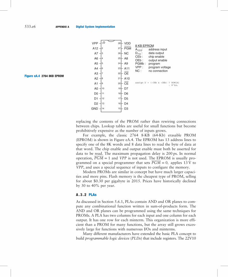
replacing the contents of the PROM rather than rewiring connectionsbetween chips. Lookup tables are useful for small functions but becomeprohibitively expensive as the number of inputs grows.
For example, the classic 2764 8-KB (64-Kb) erasable PROM(EPROM) is shown in Figure eA.4. The EPROM has 13 address lines tospecify one of the 8K words and 8 data lines to read the byte of data atthat word. The chip enable and output enable must both be asserted fordata to be read. The maximum propagation delay is 200 ps. In normaloperation, PGM = 1 and VPP is not used. The EPROM is usually pro-grammed on a special programmer that sets PGM = 0, applies 13 V toVPP, and uses a special sequence of inputs to configure the memory.
Modern PROMs are similar in concept but have much larger capaci-ties and more pins. Flash memory is the cheapest type of PROM, sellingfor about $0.30 per gigabyte in 2015. Prices have historically declinedby 30 to 40% per year.
A . 3 . 2 PLAs
As discussed in Section 5.6.1, PLAs contain AND and OR planes to com-pute any combinational function written in sum-of-products form. TheAND and OR planes can be programmed using the same techniques forPROMs. A PLA has two columns for each input and one column for eachoutput. It has one row for each minterm. This organization is more effi-cient than a PROM for many functions, but the array still grows exces-sively large for functions with numerous I/Os and minterms.
Many different manufacturers have extended the basic PLA concept tobuild programmable logic devices (PLDs) that include registers. The 22V10
A6
VPP
A12
A7
A5
A4
A3
A2
VDD
PGM
NC
A8
A9
A11
OE
A10
1
2
3
4
5
6
7
8
28
27
26
25
24
23
22
21
9
10
11
12
13
14
20
19
18
17
16
15
A0
A1
D0
D1
D2
GND
CE
D7
D6
D5
D4
D3
assign D = ( ~ CEb & ~ OEb ) ? ROM [ A ] : 8 ' bz;
8 KB EPROM A12:0: address input D7:0 : data output CEb : chip enable OEb : output enable PGMb : program VPP : program voltage NC : no connection
Figure eA.4 2764 8KB EPROM
533.e6 APPENDIX A Digital System Implementation
is one of the most popular classic PLDs. It has 12 dedicated input pins and10 outputs. The outputs can come directly from the PLA or from clockedregisters on the chip. The outputs can also be fed back into the PLA. Thus,the 22V10 can directly implement FSMs with up to 12 inputs, 10 outputs,and 10 bits of state. The 22V10 costs about $2 in quantities of 100. PLDshave been rendered mostly obsolete by the rapid improvements in capacityand cost of FPGAs.
A . 3 . 3 FPGAs
As discussed in Section 5.6.2, FPGAs consist of arrays of configurablelogic elements (LEs), also called configurable logic blocks (CLBs), con-nected together with programmable wires. The LEs contain small lookuptables and flip-flops. FPGAs scale gracefully to extremely large capacities,with thousands of lookup tables. Xilinx and Altera are two of the leadingFPGA manufacturers.
Lookup tables and programmable wires are flexible enough to imple-ment any logic function. However, they are an order of magnitude lessefficient in speed and cost (chip area) than hard-wired versions of thesame functions. Thus, FPGAs often include specialized blocks, such asmemories, multipliers, and even entire microprocessors.
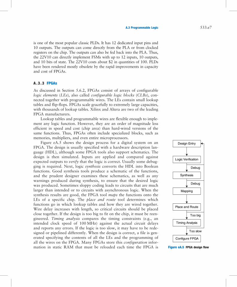
Figure eA.5 shows the design process for a digital system on anFPGA. The design is usually specified with a hardware description lan-guage (HDL), although some FPGA tools also support schematics. Thedesign is then simulated. Inputs are applied and compared againstexpected outputs to verify that the logic is correct. Usually some debug-ging is required. Next, logic synthesis converts the HDL into Booleanfunctions. Good synthesis tools produce a schematic of the functions,and the prudent designer examines these schematics, as well as anywarnings produced during synthesis, to ensure that the desired logicwas produced. Sometimes sloppy coding leads to circuits that are muchlarger than intended or to circuits with asynchronous logic. When thesynthesis results are good, the FPGA tool maps the functions onto theLEs of a specific chip. The place and route tool determines whichfunctions go in which lookup tables and how they are wired together.Wire delay increases with length, so critical circuits should be placedclose together. If the design is too big to fit on the chip, it must be reen-gineered. Timing analysis compares the timing constraints (e.g., anintended clock speed of 100MHz) against the actual circuit delaysand reports any errors. If the logic is too slow, it may have to be rede-signed or pipelined differently. When the design is correct, a file is gen-erated specifying the contents of all the LEs and the programming ofall the wires on the FPGA. Many FPGAs store this configuration infor-mation in static RAM that must be reloaded each time the FPGA is
Design Entry
Synthesis
Logic Verification
Mapping
Timing Analysis
Configure FPGA
Place and Route
Debug
Debug
Too big
Too slow
Figure eA.5 FPGA design flow
A.3 Programmable Logic 533.e7

turned on. The FPGA can download this information from a computerin the laboratory, or can read it from a nonvolatile ROM when poweris first applied.
Example eA.1 FPGA TIMING ANALYSIS
Alyssa P. Hacker is using an FPGA to implement an M&M sorter with a colorsensor and motors to put red candy in one jar and green candy in another.Her design is implemented as an FSM, and she is using a Cyclone IV FPGA.According to the data sheet, the FPGA has the timing characteristics shown inTable eA.1.
Alyssa would like her FSM to run at 100MHz. What is the maximum number ofLEs on the critical path? What is the fastest speed at which her FSM could possi-bly run?
Solution: At 100MHz, the cycle time, Tc, is 10 ns. Alyssa uses Equation 3.14 tofigure out the minimum combinational propagation delay, tpd, at this cycle time:
tpd ≤ 10ns− ð0:199 ns+ 0:076nsÞ = 9:725 ns (A.1)
With a combined LE and wire delay of 381 ps + 246 ps = 627 ps, Alyssa’s FSM canuse at most 15 consecutive LEs (9.725/0.627) to implement the next-state logic.
The fastest speed at which an FSM will run on this Cyclone IV FPGA is when it isusing a single LE for the next state logic. The minimum cycle time is
Tc ≥ 381 ps+ 199ps+76 ps = 656 ps (A.2)
Therefore, the maximum frequency is 1.5 GHz.
Altera advertises the Cyclone IV FPGA with 14,400 LEs for $25 in2015. In large quantities, medium-sized FPGAs typically cost severaldollars. The largest FPGAs cost hundreds or even thousands of dollars.
Table eA.1 Cyclone IV timing
Name Value (ps)
tpcq 199
tsetup 76
thold 0
tpd (per LE) 381
twire (between LEs) 246
tskew 0
533.e8 APPENDIX A Digital System Implementation

The cost has declined at approximately 30% per year, so FPGAs arebecoming extremely popular.
A.4 APPLICATION-SPECIFIC INTEGRATED CIRCUITS
Application-specific integrated circuits (ASICs) are chips designed for aparticular purpose. Graphics accelerators, network interface chips, andcell phone chips are common examples of ASICs. The ASIC designerplaces transistors to form logic gates and wires the gates together. Becausethe ASIC is hardwired for a specific function, it is typically several timesfaster than an FPGA and occupies an order of magnitude less chip area(and hence cost) than an FPGA with the same function. However, themasks specifying where transistors and wires are located on the chip costhundreds of thousands of dollars to produce. The fabrication processusually requires 6 to 12 weeks to manufacture, package, and test theASICs. If errors are discovered after the ASIC is manufactured, thedesigner must correct the problem, generate new masks, and wait foranother batch of chips to be fabricated. Hence, ASICs are suitable onlyfor products that will be produced in large quantities and whose functionis well defined in advance.
Figure eA.6 shows the ASIC design process, which is similar to theFPGA design process of Figure eA.5. Logic verification is especially impor-tant because correction of errors after the masks are produced is expensive.Synthesis produces a netlist consisting of logic gates and connectionsbetween the gates; the gates in this netlist are placed, and the wires are rou-ted between gates. When the design is satisfactory, masks are generatedand used to fabricate the ASIC. A single speck of dust can ruin an ASIC,so the chips must be tested after fabrication. The fraction of manufacturedchips that work is called the yield; it is typically 50 to 90%, dependingon the size of the chip and the maturity of the manufacturing process.Finally, the working chips are placed in packages, as will be discussed inSection A.7.
A.5 DATA SHEETS
Integrated circuit manufacturers publish data sheets that describe thefunctions and performance of their chips. It is essential to read and under-stand the data sheets. One of the leading sources of errors in digital sys-tems comes from misunderstanding the operation of a chip.
Data sheets are usually available from the manufacturer’s Web site. Ifyou cannot locate the data sheet for a part and do not have clear docu-mentation from another source, don’t use the part. Some of the entriesin the data sheet may be cryptic. Often the manufacturer publishes databooks containing data sheets for many related parts. The beginning of
Design Entry
Synthesis
Logic Verification
Timing Analysis
Generate Masks
Place and Route
Debug
Debug
Too big
Too slow
Fabricate ASIC
Test ASIC
Package ASIC
Defective
Figure eA.6 ASIC design flow
A.5 Data Sheets 533.e9

the data book has additional explanatory information. This informationcan usually be found on the Web with a careful search.
This section dissects the Texas Instruments (TI) data sheet for a 74HC04inverter chip. The data sheet is relatively simple but illustrates many of themajor elements. TI still manufacturers a wide variety of 74xx-series chips.In the past, many other companies built these chips too, but the market isconsolidating as the sales decline.
Figure eA.7 shows the first page of the data sheet. Some of the key sec-tions are highlighted in blue. The title is SN54HC04, SN74HC04 HEXINVERTERS. HEX INVERTERS means that the chip contains six inver-ters. SN indicates that TI is the manufacturer. Other manufacture codesinclude MC for Motorola and DM for National Semiconductor. You cangenerally ignore these codes, because all of the manufacturers build compa-tible 74xx-series logic. HC is the logic family (high speed CMOS). Thelogic family determines the speed and power consumption of the chip,but not the function. For example, the 7404, 74HC04, and 74LS04 chipsall contain six inverters, but they differ in performance and cost. Otherlogic families are discussed in Section A.6. The 74xx chips operate acrossthe commercial or industrial temperature range (0 to 70 °C or −40 to85 °C, respectively), whereas the 54xx chips operate across the militarytemperature range (−55 to 125 °C) and sell for a higher price but are other-wise compatible.
The 7404 is available in many different packages, and it is importantto order the one you intended when you make a purchase. The packagesare distinguished by a suffix on the part number. N indicates a plasticdual inline package (PDIP), which fits in a breadboard or can be solderedin through-holes in a printed circuit board. Other packages are discussedin Section A.7.
The function table shows that each gate inverts its input. If A isHIGH (H), Y is LOW (L) and vice versa. The table is trivial in this casebut is more interesting for more complex chips.
Figure eA.8 shows the second page of the data sheet. The logic diagramindicates that the chip contains inverters. The absolute maximum sectionindicates conditions beyond which the chip could be destroyed. In particu-lar, the power supply voltage (VCC, also called VDD in this book) shouldnot exceed 7 V. The continuous output current should not exceed 25mA.The thermal resistance or impedance, θJA, is used to calculate the tempera-ture rise caused by the chip’s dissipating power. If the ambient temperaturein the vicinity of the chip is TA and the chip dissipates Pchip, then the tem-perature on the chip itself at its junction with the package is
TJ = TA +Pchip θJA (A.3)
For example, if a 7404 chip in a plastic DIP package is operating in a hotbox at 50 °C and consumes 20mW, the junction temperature will climb
533.e10 APPENDIX A Digital System Implementation

SCLS078D – DECEMBER 1982 – REVISED JULY 2003
POST OFFICE BOX 655303 • DALLAS, TEXAS 75265
Wide Operating Voltage Range of 2 V to 6 V
Outputs Can Drive Up To 10 LSTTL Loads
Low Power Consumption, 20-μA Max ICC
Typical tpd = 8 ns
±4-mA Output Drive at 5 V
Low Input Current of 1 μA Max
1
2
3
4
5
6
7
14
13
12
11
10
9
8
1A1Y2A2Y3A3Y
GND
VCC6A6Y5A5Y4A4Y
SN54HC04 . . . J OR W PACKAGESN74HC04 . . . D, N, NS, OR PW PACKAGE
(TOPVIEW)
3 2 1 20 19
9 10 11 12 13
4
5
6
7
8
18
17
16
15
14
6YNC5ANC5Y
2ANC2YNC3A
Y1 A1C
NY4 A4
VC
CA 6
Y3 DN
GC
N
SN54HC04 . . . FK PACKAGE(TOPVIEW)
NC – No internal connection
description/ordering information
ORDERING INFORMATION
TA PACKAGE† ORDERABLEPARTNUMBER
TOP-SIDEMARKING
PDIP – N Tube of 25 SN74HC04N SN74HC04N
Tube of 50 SN74HC04D
SOIC – DReel of 2500 SN74HC04DR HC04
Reel of 250 SN74HC04DT–40°C to 85°C
SOP – NS Reel of 2000 SN74HC04NSR HC04
Tube of 90 SN74HC04PW
TSSOP – PW Reel of 2000 SN74HC04PWR HC04
Reel of 250 SN74HC04PWT
CDIP – J Tube of 25 SNJ54HC04J SNJ54HC04J
–55°C to 125°C CFP – W Tube of 150 SNJ54HC04W SNJ54HC04W
LCCC – FK Tube of 55 SNJ54HC04FK SNJ54HC04FK† Package drawings, standard packing quantities, thermal data, symbolization, and PCB design guidelines areavailable at www.ti.com/sc/package.
FUNCTION TABLE(each inverter)
INPUTA
OUTPUTY
H L
L H
Please be aware that an important notice concerning availability, standard warranty, and use in critical applications ofTexas Instruments semiconductor products and disclaimers there to appears at the end of this data sheet.
Copyright (c)2003, Texas Instruments IncorporatedPRODUCTION DATA information is current as of publication date.Products conform to specifications per the terms of Texas Instrumentsstandard warranty. Production processing does not necessarily includetesting of all parameters.
On products compliant to MIL-PRF-38535, all parameters are tested unless otherwise noted. On all other products, productionprocessing does not necessarily include testing of all parameters.
SN54HC04, SN74HC04HEX INVERTERS
The ’HC04 devices contain six independent inverters. They perform the Boolean function Y = Ain positive logic.
Figure eA.7 7404 data sheet page 1
A.5 Data Sheets 533.e11

SN54HC04, SN74HC04HEX INVERTERS
SCLS078D – DECEMBER 1982 – REVISED JULY 2003
POST OFFICE BOX 655303 • DALLAS, TEXAS 75265
logic diagram (positive logic)
YA
absolute maximum ratings over operating free-air temperature range (unless otherwise noted)†
Supply voltage range, VCC –0.5 V to 7 V. . . . . . . . . . . . . . . . . . . . . . . . . . . . . . . . . . . . . . . . . . . . . . . . . . . . . . . . . .Input clamp current, IIK (VI < 0 or VI > VCC) (see Note 1) ±20 mA. . . . . . . . . . . . . . . . . . . . . . . . . . . . . . . . . . . .Output clamp current, IOK (VO < 0 or VO > VCC) (see Note 1) ±20 mA. . . . . . . . . . . . . . . . . . . . . . . . . . . . . . . .Continuous output current, IO (VO = 0 to VCC) ±25 mA. . . . . . . . . . . . . . . . . . . . . . . . . . . . . . . . . . . . . . . . . . . . . .Continuous current through VCC or GND ±50 mA. . . . . . . . . . . . . . . . . . . . . . . . . . . . . . . . . . . . . . . . . . . . . . . . . . .Package thermal impedance, θJA 86° C/WegakcapD:)2etoNees( . . . . . . . . . . . . . . . . . . . . . . . . . . . . . . . . . . .
80° C/WegakcapN . . . . . . . . . . . . . . . . . . . . . . . . . . . . . . . . . . .76° C/WegakcapSN . . . . . . . . . . . . . . . . . . . . . . . . . . . . . . . . .
131° C/WegakcapWP . . . . . . . . . . . . . . . . . . . . . . . . . . . . . . . .Storage temperature range, Tstg –65° C to 150° C. . . . . . . . . . . . . . . . . . . . . . . . . . . . . . . . . . . . . . . . . . . . . . . . . . .
† Stresses beyond those listed under “absolute maximum ratings” may cause permanent damage to the device. These are stress ratings only, andfunctional operation of the device at these or any other conditions beyond those indicated under “recommended operating conditions” is notimplied. Exposure to absolute-maximum-rated conditions for extended periods may affect device reliability.
NOTES: 1. The input and output voltage ratings may be exceeded if the input and output current ratings are observed.2. The package thermal impedance is calculated in accordance with JESD 51-7.
recommended operating conditions (see Note 3)
SN54HC04 SN74HC04UNIT
MIN NOM MAX MIN NOM MAXUNIT
VCC Supply voltage 2 5 6 2 5 6 V
VCC = 2 V 1.5 1.5
VIH High-level input voltage VCC = 4.5 V 3.15 3.15 V
VCC = 6 V 4.2 4.2
VCC = 2 V 0.5 0.5
VIL Low-level input voltage VCC = 4.5 V 1.35 1.35 V
VCC = 6 V 1.8 1.8
VI Input voltage 0 VCC 0 VCC V
VO Output voltage 0 VCC 0 VCC V
VCC = 2 V 1000 1000
Δt /Δv Input transition rise/fall time VCC = 4.5 V 500 500 ns
VCC = 6 V 400 400
TA Operating free-air temperature –55 125 –40 85 ° C
NOTE 3: All unused inputs of the device must be held at VCC or GND to ensure proper device operation. Refer to the TI application report,Implications of Slow or Floating CMOS Inputs, literature number SCBA004.
TEXASINSTRUMENTS
Figure eA.8 7404 data sheet page 2
533.e12 APPENDIX A Digital System Implementation
to 50 °C + 0.02 W × 80 °C/W= 51.6 °C. Internal power dissipation is sel-dom important for 74xx-series chips, but it becomes important for mod-ern chips that dissipate tens of watts or more.
The recommended operating conditions define the environment inwhich the chip should be used. Within these conditions, the chip shouldmeet specifications. These conditions are more stringent than the absolutemaximums. For example, the power supply voltage should be between 2and 6 V. The input logic levels for the HC logic family depend on VDD.Use the 4.5 V entries when VDD= 5 V, to allow for a 10% droop in thepower supply caused by noise in the system.
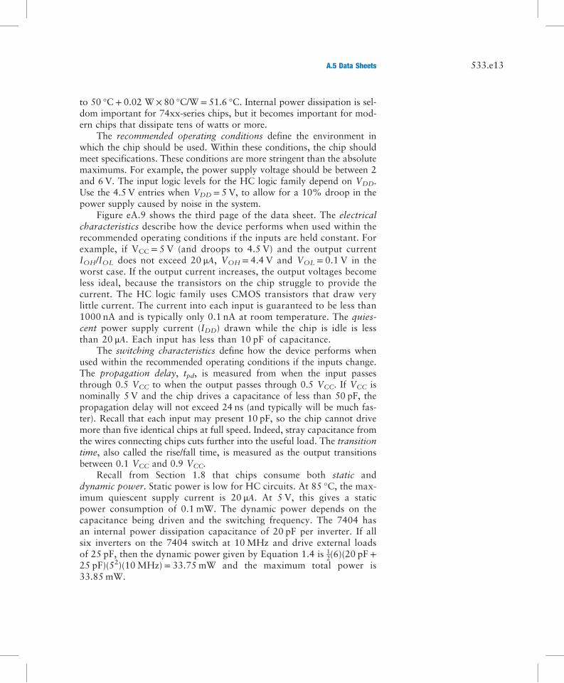
Figure eA.9 shows the third page of the data sheet. The electricalcharacteristics describe how the device performs when used within therecommended operating conditions if the inputs are held constant. Forexample, if VCC = 5 V (and droops to 4.5 V) and the output currentIOH/IOL does not exceed 20 μΑ, VOH = 4.4 V and VOL = 0.1 V in theworst case. If the output current increases, the output voltages becomeless ideal, because the transistors on the chip struggle to provide thecurrent. The HC logic family uses CMOS transistors that draw verylittle current. The current into each input is guaranteed to be less than1000 nA and is typically only 0.1 nA at room temperature. The quies-cent power supply current (IDD) drawn while the chip is idle is lessthan 20 μΑ. Each input has less than 10 pF of capacitance.
The switching characteristics define how the device performs whenused within the recommended operating conditions if the inputs change.The propagation delay, tpd, is measured from when the input passesthrough 0.5 VCC to when the output passes through 0.5 VCC. If VCC isnominally 5 V and the chip drives a capacitance of less than 50 pF, thepropagation delay will not exceed 24 ns (and typically will be much fas-ter). Recall that each input may present 10 pF, so the chip cannot drivemore than five identical chips at full speed. Indeed, stray capacitance fromthe wires connecting chips cuts further into the useful load. The transitiontime, also called the rise/fall time, is measured as the output transitionsbetween 0.1 VCC and 0.9 VCC.
Recall from Section 1.8 that chips consume both static anddynamic power. Static power is low for HC circuits. At 85 °C, the max-imum quiescent supply current is 20 μΑ. At 5 V, this gives a staticpower consumption of 0.1 mW. The dynamic power depends on thecapacitance being driven and the switching frequency. The 7404 hasan internal power dissipation capacitance of 20 pF per inverter. If allsix inverters on the 7404 switch at 10MHz and drive external loadsof 25 pF, then the dynamic power given by Equation 1.4 is 1
2(6)(20 pF +25 pF)(52)(10MHz) = 33.75 mW and the maximum total power is33.85 mW.
A.5 Data Sheets 533.e13
SN54HC04, SN74HC04HEX INVERTERS
SCLS078D – DECEMBER 1982 – REVISED JULY 2003
POST OFFICE BOX 655303 • DALLAS, TEXAS 75265
TEXASINSTRUMENTS
electrical characteristics over recommended operating free-air temperature range (unlessotherwise noted)
PARAMETER TEST CONDITIONS VCC
TA = 25 °C SN54HC04 SN74HC04UNIT
MIN TYP MAX MIN MAX MIN MAXUNIT
2 V 1.9 1.998 1.9 1.9IOH = –20 μA
IOL = 20 μA
4.5V 4.4 4.499 4.4 4.4VOH
VOL
VI = VIH or VIL
VI = VIH or VIL
VI = VCC or 0
VI = VCC or 0,
6 V 5.9 5.999 5.9 5.9 VIOH = –4 mA
IOL = 4 mA
4.5V 3.98 4.3 3.7 3.84IOH = –5.2 mA
IOL = 5.2 mA
6 V 5.48 5.8 5.2 5.34
2 V 0.002 0.1 0.1 0.1
4.5V 0.001 0.1 0.1 0.1
6 V 0.001 0.1 0.1 0.1 V
4.5V 0.17 0.26 0.4 0.33
6 V 0.15 0.26 0.4 0.33II 6 V ±0.1 ±100 ±1000 ±1000 nAICC IO = 0 6 V 2 40 20 μACi 2 V to 6 V 3 10 10 10 pF
switching characteristics over recommended operating free-air temperature range, CL = 50 pF(unless otherwise noted) (see Figure 1)
FROM TO VCCTA = 25 °C SN54HC04 SN74HC04
UNITPARAMETER (INPUT) (OUTPUT) MIN TYP MAX MIN MAX MIN MAXUNIT
2 V 45 95 145 120tpd A Y 4.5V 9 19 29 24 ns
6 V 8 16 25 20
2 V 38 75 110 95tt Y 4.5V 8 15 22 19 ns
6 V 6 13 19 16
operating characteristics, TA = 25 °CPARAMETER TEST CONDITIONS TYP UNIT
Cpd Power dissipation capacitance per inverter No load 20 pF
Figure eA.9 7404 data sheet page 3
533.e14 APPENDIX A Digital System Implementation
A.6 LOGIC FAMILIES
The 74xx-series logic chips have been manufactured using many differenttechnologies, called logic families, that offer different speed, power, andlogic level trade-offs. Other chips are usually designed to be compatible withsome of these logic families. The original chips, such as the 7404, were builtusing bipolar transistors in a technology called Transistor-Transistor Logic(TTL). Newer technologies add one or more letters after the 74 to indicatethe logic family, such as 74LS04, 74HC04, or 74AHCT04. Table eA.2 sum-marizes the most common 5-V logic families.
Advances in bipolar circuits and process technology led to theSchottky (S) and Low-Power Schottky (LS) families. Both are faster thanTTL. Schottky draws more power, whereas Low-Power Schottky drawsless. Advanced Schottky (AS) and Advanced Low-Power Schottky (ALS)have improved speed and power compared to S and LS. Fast (F) logic isfaster and draws less power than AS. All of these families provide morecurrent for LOW outputs than for HIGH outputs and hence have
Table eA.2 Typical specifications for 5-V logic families
Bipolar / TTL CMOSCMOS / TTLCompatible
Characteristic TTL S LS AS ALS F HC AHC HCT AHCT
tpd (ns) 22 9 12 7.5 10 6 21 7.5 30 7.7
VIH (V) 2 2 2 2 2 2 3.15 3.15 2 2
VIL (V) 0.8 0.8 0.8 0.8 0.8 0.8 1.35 1.35 0.8 0.8
VOH (V) 2.4 2.7 2.7 2.5 2.5 2.5 3.84 3.8 3.84 3.8
VOL (V) 0.4 0.5 0.5 0.5 0.5 0.5 0.33 0.44 0.33 0.44
IOH (mA) 0.4 1 0.4 2 0.4 1 4 8 4 8
IOL (mA) 16 20 8 20 8 20 4 8 4 8
IIL (mA) 1.6 2 0.4 0.5 0.1 0.6 0.001 0.001 0.001 0.001
IIH (mA) 0.04 0.05 0.02 0.02 0.02 0.02 0.001 0.001 0.001 0.001
IDD (mA) 33 54 6.6 26 4.2 15 0.02 0.02 0.02 0.02
CPd (pF) n/a 20 12 20 14
cost* (US $) obsolete 0.63 0.25 0.53 0.32 0.22 0.12 0.12 0.12 0.12
* Per unit in quantities of 1000 for the 7408 from Texas Instruments in 2012.
A.6 Logic Families 533.e15
asymmetric logic levels. They conform to the “TTL” logic levels: VIH= 2V,VIL= 0.8 V, VOH> 2.4V, and VOL< 0.5V.
As CMOS circuits matured in the 1980s and 1990s, they becamepopular because they draw very little power supply or input current.The High Speed CMOS (HC) and Advanced High Speed CMOS (AHC)families draw almost no static power. They also deliver the same currentfor HIGH and LOW outputs. They conform to the “CMOS” logic levels:VIH= 3.15 V, VIL= 1.35 V, VOH > 3.8 V, and VOL< 0.44 V. Unfortu-nately, these levels are incompatible with TTL circuits, because a TTLHIGH output of 2.4 V may not be recognized as a legal CMOS HIGHinput. This motivates the use of High Speed TTL-compatible CMOS(HCT) and Advanced High Speed TTL-compatible CMOS (AHCT),which accept TTL input logic levels and generate valid CMOS outputlogic levels. These families are slightly slower than their pure CMOScounterparts. All CMOS chips are sensitive to electrostatic discharge(ESD) caused by static electricity. Ground yourself by touching a largemetal object before handling CMOS chips, lest you zap them.
The 74xx-series logic is inexpensive. The newer logic families areoften cheaper than the obsolete ones. The LS family is widely availableand robust and is a popular choice for laboratory or hobby projects thathave no special performance requirements.
The 5-V standard collapsed in the mid-1990s, when transistorsbecame too small to withstand the voltage. Moreover, lower voltageoffers lower power consumption. Now 3.3, 2.5, 1.8, 1.2, and even lowervoltages are commonly used. The plethora of voltages raises challenges incommunicating between chips with different power supplies. Table eA.3lists some of the low-voltage logic families. Not all 74xx parts are avail-able in all of these logic families.
All of the low-voltage logic families use CMOS transistors, theworkhorse of modern integrated circuits. They operate over a widerange of VDD, but the speed degrades at lower voltage. Low-VoltageCMOS (LVC) logic and Advanced Low-Voltage CMOS (ALVC) logicare commonly used at 3.3, 2.5, or 1.8 V. LVC withstands inputs up to5.5 V, so it can receive inputs from 5-V CMOS or TTL circuits.Advanced Ultra-Low-Voltage CMOS (AUC) is commonly used at2.5, 1.8, or 1.2 V and is exceptionally fast. Both ALVC and AUCwithstand inputs up to 3.6 V, so they can receive inputs from 3.3-Vcircuits.
FPGAs often offer separate voltage supplies for the internal logic,called the core, and for the input/output (I/O) pins. As FPGAs haveadvanced, the core voltage has dropped from 5 to 3.3, 2.5, 1.8, and 1.2 Vto save power and avoid damaging the very small transistors. FPGAs haveconfigurable I/Os that can operate at many different voltages, so as to becompatible with the rest of the system.
533.e16 APPENDIX A Digital System Implementation

A.7 PACKAGING AND ASSEMBLY
Integrated circuits are typically placed in packages made of plastic orceramic. The packages serve a number of functions, including connectingthe tiny metal I/O pads of the chip to larger pins in the package for ease ofconnection, protecting the chip from physical damage, and spreading theheat generated by the chip over a larger area to help with cooling. Thepackages are placed on a breadboard or printed circuit board and wiredtogether to assemble the system.
PackagesFigure eA.10 shows a variety of integrated circuit packages. Packages canbe generally categorized as through-hole or surface mount (SMT).Through-hole packages, as their name implies, have pins that can beinserted through holes in a printed circuit board or into a socket. Dualinline packages (DIPs) have two rows of pins with 0.1-inch spacingbetween pins. Pin grid arrays (PGAs) support more pins in a smallerpackage by placing the pins under the package. SMT packages are sol-dered directly to the surface of a printed circuit board without usingholes. Pins on SMT parts are called leads. The thin small outline package(TSOP) has two rows of closely spaced leads (typically 0.02-inch spac-ing). Plastic leaded chip carriers (PLCCs) have J-shaped leads on all four
Table eA.3 Typical specifications for low-voltage logic families
LVC ALVC AUC
Vdd (V) 3.3 2.5 1.8 3.3 2.5 1.8 2.5 1.8 1.2
tpd (ns) 4.1 6.9 9.8 2.8 3 ?* 1.8 2.3 3.4
VIH (V) 2 1.7 1.17 2 1.7 1.17 1.7 1.17 0.78
VIL (V) 0.8 0.7 0.63 0.8 0.7 0.63 0.7 0.63 0.42
VOH (V) 2.2 1.7 1.2 2 1.7 1.2 1.8 1.2 0.8
VOL (V) 0.55 0.7 0.45 0.55 0.7 0.45 0.6 0.45 0.3
IO (mA) 24 8 4 24 12 12 9 8 3
II (mA) 0.02 0.005 0.005
IDD (mA) 0.01 0.01 0.01
Cpd (pF) 10 9.8 7 27.5 23 ?* 17 14 14
cost (US $) 0.17 0.20 not available
*Delay and capacitance not available at the time of writing.
A.7 Packaging and Assembly 533.e17

sides, with 0.05-inch spacing. They can be soldered directly to a board orplaced in special sockets. Quad flat packs (QFPs) accommodate a largenumber of pins using closely spaced legs on all four sides. Ball grid arrays(BGAs) eliminate the legs altogether. Instead, they have hundreds of tinysolder balls on the underside of the package. They are carefully placedover matching pads on a printed circuit board, then heated so that thesolder melts and joins the package to the underlying board.
BreadboardsDIPs are easy to use for prototyping, because they can be placed in abreadboard. A breadboard is a plastic board containing rows of sockets,as shown in Figure eA.11. All five holes in a row are connected together.Each pin of the package is placed in a hole in a separate row. Wires canbe placed in adjacent holes in the same row to make connections to thepin. Breadboards often provide separate columns of connected holes run-ning the height of the board to distribute power and ground.
Figure eA.11 shows a breadboard containing a majority gate builtwith a 74LS08 AND chip and a 74LS32 OR chip. The schematic of thecircuit is shown in Figure eA.12. Each gate in the schematic is labeledwith the chip (08 or 32) and the pin numbers of the inputs and outputs(see Figure eA.1). Observe that the same connections are made on thebreadboard. The inputs are connected to pins 1, 2, and 5 of the 08 chip,and the output is measured at pin 6 of the 32 chip. Power and ground areconnected to pins 14 and 7, respectively, of each chip, from the verticalpower and ground columns that are attached to the banana plug recepta-cles, Vb and Va. Labeling the schematic in this way and checking off con-nections as they are made is a good way to reduce the number of mistakesmade during breadboarding.
Unfortunately, it is easy to accidentally plug a wire in the wrong holeor have a wire fall out, so breadboarding requires a great deal of care(and usually some debugging in the laboratory). Breadboards are suitedonly to prototyping, not production.
Figure eA.10 Integrated circuitpackages
533.e18 APPENDIX A Digital System Implementation

Printed Circuit BoardsInstead of breadboarding, chip packages may be soldered to a printed cir-cuit board (PCB). The PCB is formed of alternating layers of conductingcopper and insulating epoxy. The copper is etched to form wires calledtraces. Holes called vias are drilled through the board and plated withmetal to connect between layers. PCBs are usually designed with compu-ter-aided design (CAD) tools. You can etch and drill your own simpleboards in the laboratory, or you can send the board design to a specia-lized factory for inexpensive mass production. Factories have turnaroundtimes of days (or weeks, for cheap mass production runs) and typicallycharge a few hundred dollars in setup fees and a few dollars per boardfor moderately complex boards built in large quantities.
GND
Rows of 5 pins areinternally connected
VDD Figure eA.11 Majority circuit onbreadboard
08
08
08
32
32
1BC
Y
23
4
56
89
10
1
2
3
4
56
A
Figure eA.12 Majority gateschematic with chips and pinsidentified
A.7 Packaging and Assembly 533.e19

PCB traces are normally made of copper because of its low resistance.The traces are embedded in an insulating material, usually a green, fire-resistant plastic called FR4. A PCB also typically has copper power andground layers, called planes, between signal layers. Figure eA.13 showsa cross-section of a PCB. The signal layers are on the top and bottom,and the power and ground planes are embedded in the center of theboard. The power and ground planes have low resistance, so they distri-bute stable power to components on the board. They also make the capa-citance and inductance of the traces uniform and predictable.
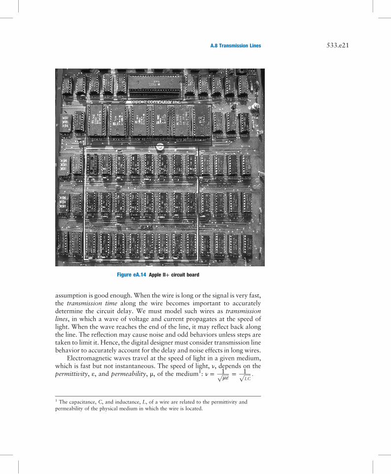
Figure eA.14 shows a PCB for a 1970s vintage Apple II+ computer.At the top is a 6502 microprocessor. Beneath are six 16-Kb ROM chipsforming 12 KB of ROM containing the operating system. Three rows ofeight 16-Kb DRAM chips provide 48 KB of RAM. On the right are sev-eral rows of 74xx-series logic for memory address decoding and otherfunctions. The lines between chips are traces that wire the chips together.The dots at the ends of some of the traces are vias filled with metal.
Putting It All TogetherMost modern chips with large numbers of inputs and outputs use SMTpackages, especially QFPs and BGAs. These packages require a printedcircuit board rather than a breadboard. Working with BGAs is especiallychallenging because they require specialized assembly equipment. More-over, the balls cannot be probed with a voltmeter or oscilloscope duringdebugging in the laboratory, because they are hidden under the package.
In summary, the designer needs to consider packaging early on to deter-mine whether a breadboard can be used during prototyping and whetherBGA parts will be required. Professional engineers rarely use breadboardswhen they are confident of connecting chips together correctly withoutexperimentation.
A.8 TRANSMISSION LINES
We have assumed so far that wires are equipotential connections that havea single voltage along their entire length. Signals actually propagatealong wires at the speed of light in the form of electromagnetic waves. Ifthe wires are short enough or the signals change slowly, the equipotential
Signal Layer
Signal Layer
Power Plane
Ground Plane
Copper Trace Insulator
Figure eA.13 Printed circuitboard cross-section
533.e20 APPENDIX A Digital System Implementation
assumption is good enough. When the wire is long or the signal is very fast,the transmission time along the wire becomes important to accuratelydetermine the circuit delay. We must model such wires as transmissionlines, in which a wave of voltage and current propagates at the speed oflight. When the wave reaches the end of the line, it may reflect back alongthe line. The reflection may cause noise and odd behaviors unless steps aretaken to limit it. Hence, the digital designer must consider transmission linebehavior to accurately account for the delay and noise effects in long wires.
Electromagnetic waves travel at the speed of light in a given medium,which is fast but not instantaneous. The speed of light, ν, depends on thepermittivity, ε, and permeability, μ, of the medium1: ν = 1ffiffiffiffiffi
μεp = 1ffiffiffiffiffi
LCp :
Figure eA.14 Apple II+ circuit board
1 The capacitance, C, and inductance, L, of a wire are related to the permittivity andpermeability of the physical medium in which the wire is located.
A.8 Transmission Lines 533.e21

The speed of light in free space is v= c = 3 × 10⁸m/s. Signals in a PCBtravel at about half this speed, because the FR4 insulator has four timesthe permittivity of air. Thus, PCB signals travel at about 1.5 × 10⁸ m/s,or 15 cm/ns. The time delay for a signal to travel along a transmission lineof length l is
td = lv (A.4)
The characteristic impedance of a transmission line, Z0 (pronounced“Z-naught”), is the ratio of voltage to current in a wave traveling alongthe line: Z0=V/I. It is not the resistance of the wire (a good transmissionline in a digital system typically has negligible resistance). Z0 depends onthe inductance and capacitance of the line (see the derivation in SectionA.8.7) and typically has a value of 50 to 75 Ω.
Z0 =
ffiffiffiffiLC
r(A.5)
Figure eA.15 shows the symbol for a transmission line. The symbolresembles a coaxial cable with an inner signal conductor and an outergrounded conductor like that used in television cable wiring.
The key to understanding the behavior of transmission lines is tovisualize the wave of voltage propagating along the line at the speed oflight. When the wave reaches the end of the line, it may be absorbed orreflected, depending on the termination or load at the end. Reflectionstravel back along the line, adding to the voltage already on the line.Terminations are classified as matched, open, short, or mismatched. Thefollowing sections explore how a wave propagates along the line andwhat happens to the wave when it reaches the termination.
A . 8 . 1 Matched Termination
Figure eA.16 shows a transmission line of length l with a matched termi-nation, which means that the load impedance, ZL, is equal to the charac-teristic impedance, Z0. The transmission line has a characteristicimpedance of 50 Ω. One end of the line is connected to a voltage source
I
V
–
+
Z0 =C
L
Figure eA.15 Transmission linesymbol
533.e22 APPENDIX A Digital System Implementation
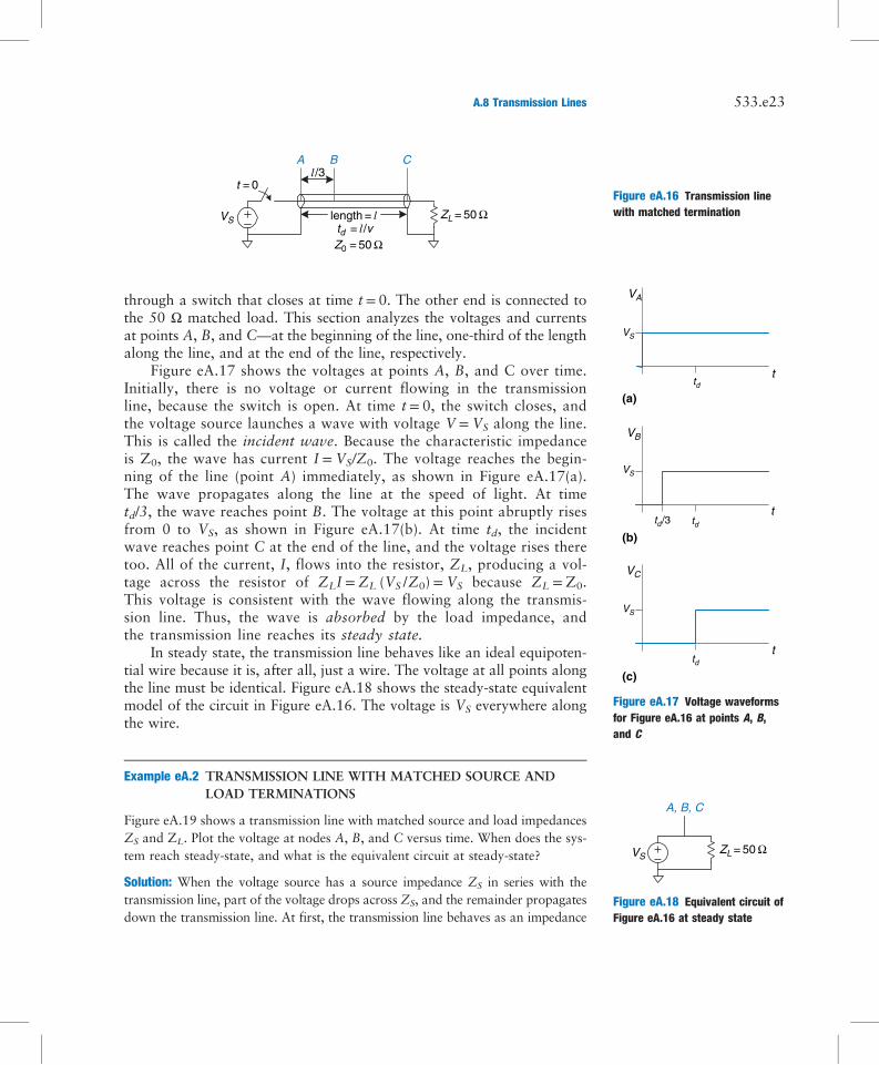
through a switch that closes at time t= 0. The other end is connected tothe 50 Ω matched load. This section analyzes the voltages and currentsat points A, B, and C—at the beginning of the line, one-third of the lengthalong the line, and at the end of the line, respectively.
Figure eA.17 shows the voltages at points A, B, and C over time.Initially, there is no voltage or current flowing in the transmissionline, because the switch is open. At time t = 0, the switch closes, andthe voltage source launches a wave with voltage V = VS along the line.This is called the incident wave. Because the characteristic impedanceis Z0, the wave has current I = VS/Z0. The voltage reaches the begin-ning of the line (point A) immediately, as shown in Figure eA.17(a).The wave propagates along the line at the speed of light. At timetd/3, the wave reaches point B. The voltage at this point abruptly risesfrom 0 to VS, as shown in Figure eA.17(b). At time td, the incidentwave reaches point C at the end of the line, and the voltage rises theretoo. All of the current, I, flows into the resistor, ZL, producing a vol-tage across the resistor of ZLI = ZL (VS /Z0) = VS because ZL = Z0.This voltage is consistent with the wave flowing along the transmis-sion line. Thus, the wave is absorbed by the load impedance, andthe transmission line reaches its steady state.
In steady state, the transmission line behaves like an ideal equipoten-tial wire because it is, after all, just a wire. The voltage at all points alongthe line must be identical. Figure eA.18 shows the steady-state equivalentmodel of the circuit in Figure eA.16. The voltage is VS everywhere alongthe wire.
Example eA.2 TRANSMISSION LINE WITH MATCHED SOURCE ANDLOAD TERMINATIONS
Figure eA.19 shows a transmission line with matched source and load impedancesZS and ZL. Plot the voltage at nodes A, B, and C versus time. When does the sys-tem reach steady-state, and what is the equivalent circuit at steady-state?
Solution: When the voltage source has a source impedance ZS in series with thetransmission line, part of the voltage drops across ZS, and the remainder propagatesdown the transmission line. At first, the transmission line behaves as an impedance
VS
t = 0
Z0 = 50 Ω
length = l td = l /v
A CBl /3
ZL = 50 Ω
Figure eA.16 Transmission linewith matched termination
(a)
ttd
VA
VS
(c)
t
VS
td
VC
(b)
t
VS
td /3 td
VB
Figure eA.17 Voltage waveformsfor Figure eA.16 at points A, B,and C
VSZL = 50 Ω
A, B, C
Figure eA.18 Equivalent circuit ofFigure eA.16 at steady state
A.8 Transmission Lines 533.e23
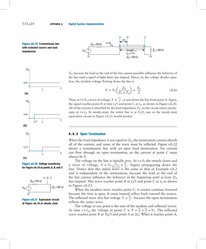
Z0, because the load at the end of the line cannot possibly influence the behavior ofthe line until a speed of light delay has elapsed. Hence, by the voltage divider equa-tion, the incident voltage flowing down the line is
V = VSZ0
Z0 +ZS
� �=
VS
2(A.6)
Thus, at t= 0, a wave of voltage,V =VS2, is sent down the line from pointA. Again,
the signal reaches point B at time td/3 and point C at td, as shown in Figure eA.20.All of the current is absorbed by the load impedanceZL, so the circuit enters steady-state at t= td. In steady-state, the entire line is at VS/2, just as the steady-stateequivalent circuit in Figure eA.21 would predict.
A . 8 . 2 Open Termination
When the load impedance is not equal to Z0, the termination cannot absorball of the current, and some of the wave must be reflected. Figure eA.22shows a transmission line with an open load termination. No currentcan flow through an open termination, so the current at point C mustalways be 0.
The voltage on the line is initially zero. At t= 0, the switch closes anda wave of voltage, V = VS
Z0
Z0 +ZS= VS
2, begins propagating down the
line. Notice that this initial wave is the same as that of Example eA.2and is independent of the termination, because the load at the end ofthe line cannot influence the behavior at the beginning until at least 2tdhas elapsed. This wave reaches point B at td/3 and point C at td as shownin Figure eA.23.
When the incident wave reaches point C, it cannot continue forwardbecause the wire is open. It must instead reflect back toward the source.The reflected wave also has voltage V = VS
2, because the open termination
reflects the entire wave.The voltage at any point is the sum of the incident and reflected waves.
At time t = td, the voltage at point C is V = VS
2+ VS
2=VS: The reflected
wave reaches point B at 5td/3 and point A at 2td. When it reaches point A,
VS
t = 0
Z0 = 50 Ω
ZL = 50 Ω
ZS = 50 Ω
length = l td = l /v
A CBl /3
Figure eA.19 Transmission linewith matched source and loadimpedances
t
VA
(a)
VS/2
td
t
(b)
td / 3
VS/2
VB
t
(c)
td
VC
VS / 2
td
Figure eA.20 Voltage waveformsfor Figure eA.19 at points A, B, and C
ZL = 50 Ω
ZS = 50 ΩA, B, C
VS
Figure eA.21 Equivalent circuitof Figure eA.19 at steady state
533.e24 APPENDIX A Digital System Implementation

the wave is absorbed by the source termination impedance that matches thecharacteristic impedance of the line. Thus, the system reaches steady state attime t= 2td, and the transmission line becomes equivalent to an equipoten-tial wire with voltage VS and current I= 0.
A . 8 . 3 Short Termination
Figure eA.24 shows a transmission line terminated with a short circuit toground. Thus, the voltage at point C must always be 0.
As in the previous examples, the voltages on the line are initially 0.Whenthe switch closes, a wave of voltage, V = VS
2, begins propagating down
the line (Figure eA.25). When it reaches the end of the line, it must reflectwith opposite polarity. The reflected wave, with voltage V = −VS
2, adds
to the incident wave, ensuring that the voltage at point C remains 0. Thereflectedwave reaches the source at time t= 2td and is absorbed by the sourceimpedance. At this point, the system reaches steady state, and the transmis-sion line is equivalent to an equipotential wire with voltage V= 0.
A . 8 . 4 Mismatched Termination
The termination impedance is said to be mismatched when it does notequal the characteristic impedance of the line. In general, when an inci-dent wave reaches a mismatched termination, part of the wave isabsorbed and part is reflected. The reflection coefficient kr indicates thefraction of the incident wave Vi that is reflected: Vr= krVi.
Section A.8.8 derives the reflection coefficient using conservation ofcurrent arguments. It shows that, when an incident wave flowing along
VS
t = 0
Z0 = 50 Ω
length = l td = l /v
A CBl /3
ZS = 50 Ω Figure eA.22 Transmission linewith open load termination
t
VS /2
VS
5td /3td
/3 td
VB
t
VS
td
VC
(c)
(b)
(a)
ttd
VA
VS /2
VS
2td
Figure eA.23 Voltage waveformsfor Figure eA.22 at pointsA, B, and C
VS
t = 0
Z0 = 50 Ω
length = l td = l /v
A CBl /3
ZS = 50 Ω
Figure eA.24 Transmission line with short termination
A.8 Transmission Lines 533.e25
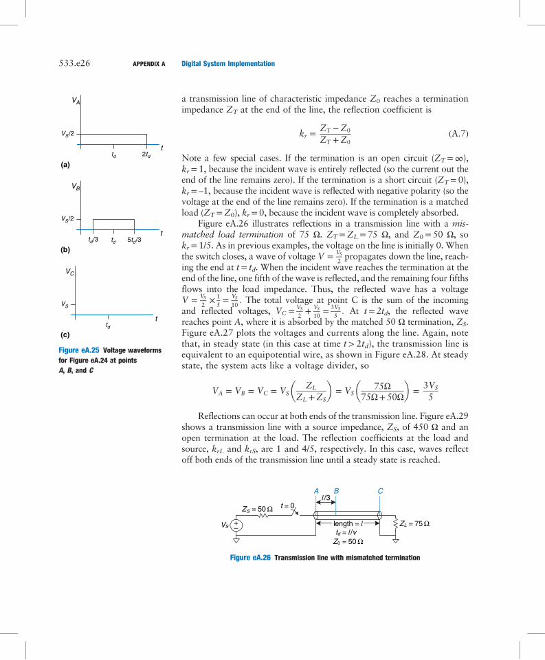
a transmission line of characteristic impedance Z0 reaches a terminationimpedance ZT at the end of the line, the reflection coefficient is
kr =ZT −Z0
ZT +Z0(A.7)
Note a few special cases. If the termination is an open circuit (ZT=∞),kr= 1, because the incident wave is entirely reflected (so the current out theend of the line remains zero). If the termination is a short circuit (ZT= 0),kr= –1, because the incident wave is reflected with negative polarity (so thevoltage at the end of the line remains zero). If the termination is a matchedload (ZT=Z0), kr= 0, because the incident wave is completely absorbed.
Figure eA.26 illustrates reflections in a transmission line with a mis-matched load termination of 75 Ω. ZT=ZL= 75 Ω, and Z0= 50 Ω, sokr= 1/5. As in previous examples, the voltage on the line is initially 0. Whenthe switch closes, a wave of voltage V = VS
2propagates down the line, reach-
ing the end at t= td. When the incident wave reaches the termination at theend of the line, one fifth of the wave is reflected, and the remaining four fifthsflows into the load impedance. Thus, the reflected wave has a voltageV = VS
2× 1
5= VS
10: The total voltage at point C is the sum of the incoming
and reflected voltages, VC = VS
2+ VS
10= 3VS
5: At t= 2td, the reflected wave
reaches point A, where it is absorbed by the matched 50 Ω termination, ZS.Figure eA.27 plots the voltages and currents along the line. Again, notethat, in steady state (in this case at time t > 2td), the transmission line isequivalent to an equipotential wire, as shown in Figure eA.28. At steadystate, the system acts like a voltage divider, so
VA = VB = VC = VSZL
ZL +ZS
� �= VS
75Ω75Ω+ 50Ω
� �=
3VS
5
Reflections can occur at both ends of the transmission line. Figure eA.29shows a transmission line with a source impedance, ZS, of 450 Ω and anopen termination at the load. The reflection coefficients at the load andsource, krL and krS, are 1 and 4/5, respectively. In this case, waves reflectoff both ends of the transmission line until a steady state is reached.
ttd
VA
VS /2
2td(a)
t
VS /2
5td /3td
/3 td
VB
(b)
(c)
t
VS
td
VC
Figure eA.25 Voltage waveformsfor Figure eA.24 at pointsA, B, and C
VS
t = 0
Z0 = 50 Ω
length = ltd = l/v
A CBl /3
ZL = 75 Ω
ZS = 50 Ω
+–
Figure eA.26 Transmission line with mismatched termination
533.e26 APPENDIX A Digital System Implementation
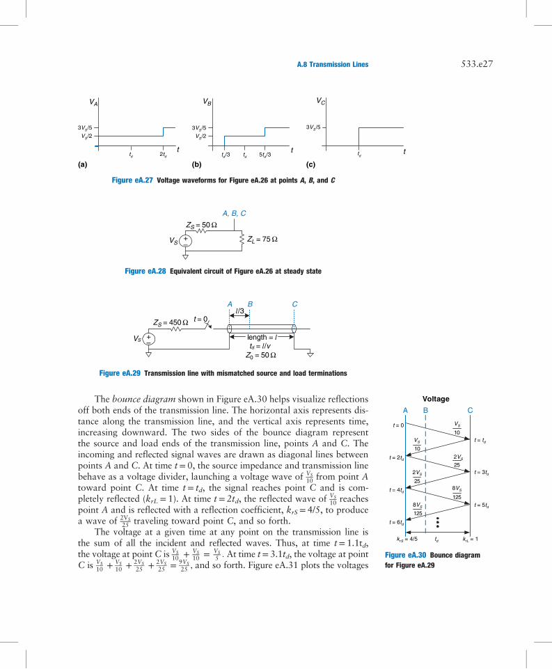
The bounce diagram shown in Figure eA.30 helps visualize reflectionsoff both ends of the transmission line. The horizontal axis represents dis-tance along the transmission line, and the vertical axis represents time,increasing downward. The two sides of the bounce diagram representthe source and load ends of the transmission line, points A and C. Theincoming and reflected signal waves are drawn as diagonal lines betweenpoints A and C. At time t= 0, the source impedance and transmission linebehave as a voltage divider, launching a voltage wave of VS
10 from point Atoward point C. At time t= td, the signal reaches point C and is com-pletely reflected (krL= 1). At time t= 2td, the reflected wave of VS
10 reachespoint A and is reflected with a reflection coefficient, krS= 4/5, to producea wave of 2VS
25 traveling toward point C, and so forth.The voltage at a given time at any point on the transmission line is
the sum of all the incident and reflected waves. Thus, at time t= 1.1td,the voltage at point C is VS
10 + VS10 = VS
5 : At time t= 3.1td, the voltage at pointC is VS
10 + VS10 + 2VS
25 + 2VS25 = 9VS
25 , and so forth. Figure eA.31 plots the voltages
ttd
VA
VS /2
3VS /5
2td
(a)
t
VB
3VS /5
VS /2
td 5td /3td
/3
(b)
ttd
VC
(c)
3VS /5
Figure eA.27 Voltage waveforms for Figure eA.26 at points A, B, and C
A, B, C
VS
ZS = 50 Ω
ZL = 75 Ω+–
Figure eA.28 Equivalent circuit of Figure eA.26 at steady state
VS
t = 0
length = ltd = l/v
A CBl /3
ZS = 450 Ω
+
Z0 = 50 Ω
–
Figure eA.29 Transmission line with mismatched source and load terminations
Voltage
A C
10VS
10
25
25
125
125
t = td
krS = 4/5
B
VS
2VS
2VS
8VS
8VS
t = 3td
t = 5td
t = 6td
t = 4td
t = 2td
t = 0
td krL = 1
Figure eA.30 Bounce diagramfor Figure eA.29
A.8 Transmission Lines 533.e27

against time. As t approaches infinity, the voltages approach steady statewith VA=VB=VC=VS.
A . 8 . 5 When to Use Transmission Line Models
Transmission line models for wires are needed whenever the wire delay,td, is longer than a fraction (e.g., 20%) of the edge rates (rise or fall times)of a signal. If the wire delay is shorter, it has an insignificant effect on thepropagation delay of the signal, and the reflections dissipate while the sig-nal is transitioning. If the wire delay is longer, it must be considered inorder to accurately predict the propagation delay and waveform of thesignal. In particular, reflections may distort the digital characteristic of awaveform, resulting in incorrect logic operations.
Recall that signals travel on a PCB at about 15 cm/ns. For TTL logic,with edge rates of 10 ns, wires must be modeled as transmission lines onlyif they are longer than 30 cm (10 ns × 15 cm/ns × 20%). PCB traces areusually less than 30 cm, so most traces can be modeled as ideal equipoten-tial wires. In contrast, many modern chips have edge rates of 2 ns or less,so traces longer than about 6 cm (about 2.5 inches) must be modeled astransmission lines. Clearly, use of edge rates that are crisper than neces-sary just causes difficulties for the designer.
Breadboards lack a ground plane, so the electromagnetic fields of eachsignal are nonuniform and difficult to model. Moreover, the fields interactwith other signals. This can cause strange reflections and crosstalk betweensignals. Thus, breadboards are unreliable above a few megahertz.
In contrast, PCBs have good transmission lines with consistent char-acteristic impedance and velocity along the entire line. As long as theyare terminated with a source or load impedance that is matched to theimpedance of the line, PCB traces do not suffer from reflections.
A . 8 . 6 Proper Transmission Line Terminations
There are two common ways to properly terminate a transmission line,shown in Figure eA.32. In parallel termination, the driver has a low impe-dance (ZS ≈ 0). A load resistor ZL with impedance Z0 is placed in parallel
t
VS
10
2525
VA
2td
7VS
16VS
4td 6td
(a)
t
3 3 3 3 3 3
10
2525
5
25
VB
VS
VS7VS
9VS16VS
td 5td 7td 11td 13td 17td
(b)
t
5
25125
VC
(c)
td 3td 5td
9VS
61VS
VS
Figure eA.31 Voltage and current waveforms for Figure eA.29
533.e28 APPENDIX A Digital System Implementation

with the load (between the input of the receiver gate and ground). Whenthe driver switches from 0 to VDD, it sends a wave with voltage VDD
down the line. The wave is absorbed by the matched load termination,and no reflections take place. In series termination, a source resistor ZS
is placed in series with the driver to raise the source impedance to Z0.The load has a high impedance (ZL ≈ ∞). When the driver switches, itsends a wave with voltage VDD/2 down the line. The wave reflects atthe open circuit load and returns, bringing the voltage on the line up toVDD. The wave is absorbed at the source termination. Both schemes aresimilar in that the voltage at the receiver transitions from 0 to VDD att= td, just as one would desire. They differ in power consumption andin the waveforms that appear elsewhere along the line. Parallel termina-tion dissipates power continuously through the load resistor when the lineis at a high voltage. Series termination dissipates no DC power, becausethe load is an open circuit. However, in series terminated lines, pointsnear the middle of the transmission line initially see a voltage of VDD/2,
A CBdrivergate
(b)
receivergate
series termination
resistor
ZL ≈ ∞
t
t
td
t
VDD
VA
VB
VC
t
t
t
V DD
VDD
VB
VC
A CB
(a)
drivergate
receivergate
paralleltermination
resistor
ZS ≈ 0
Z0
ZL = Z0
ZS = Z0
Z0
VA
VDD /2
VDD
td /3 td
VDD
td
td 2td
5td /3td /3 td
td
VDD
VDD /2
Figure eA.32 Termination schemes: (a) parallel, (b) series
A.8 Transmission Lines 533.e29

until the reflection returns. If other gates are attached to the middle of theline, they will momentarily see an illegal logic level. Therefore, seriestermination works best for point-to-point communication with a singledriver and a single receiver. Parallel termination is better for a bus withmultiple receivers, because receivers at the middle of the line never seean illegal logic level.
A . 8 . 7 Derivation of Z0*
Z0 is the ratio of voltage to current in a wave propagating along a trans-mission line. This section derives Z0; it assumes some previous knowledgeof resistor-inductor-capacitor (RLC) circuit analysis.
Imagine applying a step voltage to the input of a semi-infinite trans-mission line (so that there are no reflections). Figure eA.33 shows thesemi-infinite line and a model of a segment of the line of length dx. R,L, and C, are the values of resistance, inductance, and capacitance perunit length. Figure eA.33(b) shows the transmission line model with aresistive component, R. This is called a lossy transmission line model,because energy is dissipated, or lost, in the resistance of the wire. How-ever, this loss is often negligible, and we can simplify analysis by ignoringthe resistive component and treating the transmission line as an idealtransmission line, as shown in Figure eA.33(c).
Voltage and current are functions of time and space throughout thetransmission line, as given by Equations eA.8 and eA.9.
∂∂x
Vðx, tÞ = L ∂∂tIðx, tÞ (A.8)
∂∂x
Iðx, tÞ = C ∂∂tVðx, tÞ (A.9)
Taking the space derivative of Equation eA.8 and the time derivative ofEquation eA.9 and substituting gives Equation eA.10, the wave equation.
∂2
∂x2Vðx, tÞ = LC ∂2
∂t2Vðx, tÞ (A.10)
Z0 is the ratio of voltage to current in the transmission line, as illustratedin Figure eA.34(a). Z0 must be independent of the length of the line, becausethe behavior of the wave cannot depend on things at a distance. Because it isindependent of length, the impedancemust still equalZ0 after the addition ofa small amount of transmission line, dx, as shown in Figure eA.34(b).
xdx
(a)
Cdx
Rdx
dx
Ldx
(b)
Ldx
Cdx
dx(c)
Figure eA.33 Transmission linemodels: (a) semi-infinite cable,(b) lossy, (c) ideal
533.e30 APPENDIX A Digital System Implementation
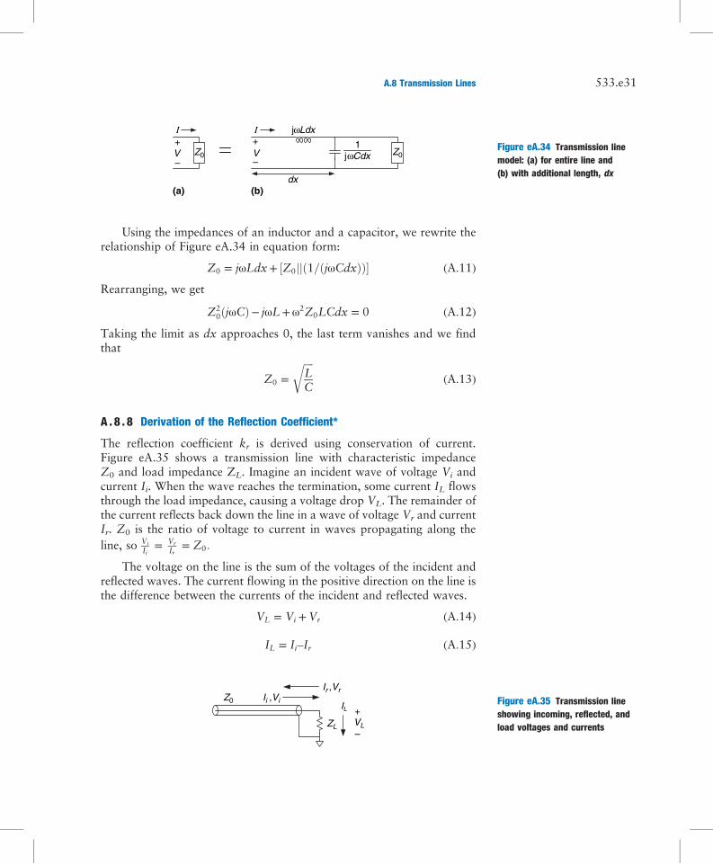
Using the impedances of an inductor and a capacitor, we rewrite therelationship of Figure eA.34 in equation form:
Z0 = jωLdx+ ½Z0jjð1=ðjωCdxÞÞ� (A.11)
Rearranging, we get
Z20ðjωCÞ− jωL+ω2Z0LCdx = 0 (A.12)
Taking the limit as dx approaches 0, the last term vanishes and we findthat
Z0 =
ffiffiffiffiLC
r(A.13)
A . 8 . 8 Derivation of the Reflection Coefficient*
The reflection coefficient kr is derived using conservation of current.Figure eA.35 shows a transmission line with characteristic impedanceZ0 and load impedance ZL. Imagine an incident wave of voltage Vi andcurrent Ii. When the wave reaches the termination, some current IL flowsthrough the load impedance, causing a voltage drop VL. The remainder ofthe current reflects back down the line in a wave of voltage Vr and currentIr. Z0 is the ratio of voltage to current in waves propagating along theline, so Vi
Ii= Vr
Ir= Z0:
The voltage on the line is the sum of the voltages of the incident andreflected waves. The current flowing in the positive direction on the line isthe difference between the currents of the incident and reflected waves.
VL = Vi +Vr (A.14)
IL = Ii–Ir (A.15)
jωLdx
dx
jωCdx1
Z0V–
+I
V–
+I
(a)
Z0
(b)
Figure eA.34 Transmission linemodel: (a) for entire line and(b) with additional length, dx
Z0
ZL
Ii ,Vi
+
–
IL
Ir ,Vr
VL
Figure eA.35 Transmission lineshowing incoming, reflected, andload voltages and currents
A.8 Transmission Lines 533.e31

Using Ohm’s law and substituting for IL, Ii , and Ir in Equation eA.15,we get
Vi +Vr
ZL=
Vi
Z0− Vr
Z0(A.16)
Rearranging, we solve for the reflection coefficient, kr:
Vr
Vi=
ZL −Z0
ZL +Z0= kr (A.17)
A . 8 . 9 Putting It All Together
Transmission lines model the fact that signals take time to propagatedown long wires because the speed of light is finite. An ideal transmissionline has uniform inductance L and capacitance C per unit length and zeroresistance. The transmission line is characterized by its characteristicimpedance Z0 and delay td which can be derived from the inductance,capacitance, and wire length. The transmission line has significant delayand noise effects on signals whose rise/fall times are less than about 5td.This means that, for systems with 2 ns rise/fall times, PCB traces longerthan about 6 cm must be analyzed as transmission lines to accuratelyunderstand their behavior.
A digital system consisting of a gate driving a long wire attached tothe input of a second gate can be modeled with a transmission line asshown in Figure eA.36. The voltage source, source impedance ΖS, andswitch model the first gate switching from 0 to 1 at time 0. The drivergate cannot supply infinite current; this is modeled by ZS. ZS is usuallysmall for a logic gate, but a designer may choose to add a resistor in serieswith the gate to raise ZS and match the impedance of the line. The inputto the second gate is modeled as ZL. CMOS circuits usually have littleinput current, so ZL may be close to infinity. The designer may alsochoose to add a resistor in parallel with the second gate, between the gateinput and ground, so that ZL matches the impedance of the line.
(a)
long wire
drivergate
receivergate
VS td , Z0
Z
–
S
(b)
receiver gatelong wiredriver gate
ZL
t = 0
+
Figure eA.36 Digital systemmodeled with transmission line
533.e32 APPENDIX A Digital System Implementation
When the first gate switches, a wave of voltage is driven onto thetransmission line. The source impedance and transmission line form a vol-tage divider, so the voltage of the incident wave is
Vi = VSZ0
Z0 +ZS(A.18)
At time td, the wave reaches the end of the line. Part is absorbed bythe load impedance, and part is reflected. The reflection coefficient krindicates the portion that is reflected: kr=Vr/Vi, where Vr is the voltageof the reflected wave and Vi is the voltage of the incident wave.
kr =ZL −Z0
ZL +Z0(A.19)
The reflected wave adds to the voltage already on the line. It reachesthe source at time 2td, where part is absorbed and part is again reflected.The reflections continue back and forth, and the voltage on the line even-tually approaches the value that would be expected if the line were a sim-ple equipotential wire.
A.9 ECONOMICS
Although digital design is so much fun that some of us would do it forfree, most designers and companies intend to make money. Therefore,economic considerations are a major factor in design decisions.
The cost of a digital system can be divided into nonrecurring engi-neering costs (NRE), and recurring costs. NRE accounts for the cost ofdesigning the system. It includes the salaries of the design team, computerand software costs, and the costs of producing the first working unit. Thefully loaded cost of a designer in the United States in 2015 (including sal-ary, health insurance, retirement plan, and a computer with design tools)was roughly $200,000 per year, so design costs can be significant. Recur-ring costs are the cost of each additional unit; this includes components,manufacturing, marketing, technical support, and shipping.
The sales price must cover not only the cost of the system but alsoother costs such as office rental, taxes, and salaries of staff who do notdirectly contribute to the design (such as the janitor and the CEO). Afterall of these expenses, the company should still make a profit.
Example eA.3 BEN TRIES TO MAKE SOME MONEY
Ben Bitdiddle has designed a crafty circuit for counting raindrops. He decides tosell the device and try to make some money, but he needs help deciding whatimplementation to use. He decides to use either an FPGA or an ASIC. The
A.9 Economics 533.e33
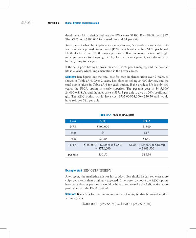
development kit to design and test the FPGA costs $1500. Each FPGA costs $17.The ASIC costs $600,000 for a mask set and $4 per chip.
Regardless of what chip implementation he chooses, Ben needs to mount the pack-aged chip on a printed circuit board (PCB), which will cost him $1.50 per board.He thinks he can sell 1000 devices per month. Ben has coerced a team of brightundergraduates into designing the chip for their senior project, so it doesn’t costhim anything to design.
If the sales price has to be twice the cost (100% profit margin), and the productlife is 2 years, which implementation is the better choice?
Solution: Ben figures out the total cost for each implementation over 2 years, asshown in Table eA.4. Over 2 years, Ben plans on selling 24,000 devices, and thetotal cost is given in Table eA.4 for each option. If the product life is only twoyears, the FPGA option is clearly superior. The per-unit cost is $445,500/24,000= $18.56, and the sales price is $37.13 per unit to give a 100% profit mar-gin. The ASIC option would have cost $732,000/24,000= $30.50 and wouldhave sold for $61 per unit.
Example eA.4 BEN GETS GREEDY
After seeing the marketing ads for his product, Ben thinks he can sell even morechips per month than originally expected. If he were to choose the ASIC option,how many devices per month would he have to sell to make the ASIC option moreprofitable than the FPGA option?
Solution: Ben solves for the minimum number of units, N, that he would need tosell in 2 years:
$600, 000+ ðN × $5:50Þ = $1500+ ðN × $18:50Þ
Table eA.4 ASIC vs FPGA costs
Cost ASIC FPGA
NRE $600,000 $1500
chip $4 $17
PCB $1.50 $1.50
TOTAL $600,000 + (24,000 × $5.50)= $732,000
$1500 + (24,000 × $18.50)= $445,500
per unit $30.50 $18.56
533.e34 APPENDIX A Digital System Implementation

Solving the equation gives N= 46,039 units, or 1919 units per month. He wouldneed to almost double his monthly sales to benefit from the ASIC solution.
Example eA.5 BEN GETS LESS GREEDY
Ben realizes that his eyes have gotten too big for his stomach, and he doesn’t thinkhe can sell more than 1000 devices per month. But he does think the product lifecan be longer than 2 years. At a sales volume of 1000 devices per month, howlong would the product life have to be to make the ASIC option worthwhile?
Solution: If Ben sells more than 46,039 units in total, the ASIC option is the bestchoice. So, Ben would need to sell at a volume of 1000 per month for at least47 months (rounding up), which is almost 4 years. By then, his product is likelyto be obsolete.
Chips are usually purchased from a distributor rather than directlyfrom the manufacturer (unless you are ordering tens of thousands ofunits). Digikey (www.digikey.com) is a leading distributor that sells awide variety of electronics. Jameco (www.jameco.com) and All Electronics(www.allelectronics.com) have eclectic catalogs that are competitivelypriced and well suited to hobbyists.
A.9 Economics 533.e35
