digital logic - gates, boolean algebra
TRANSCRIPT
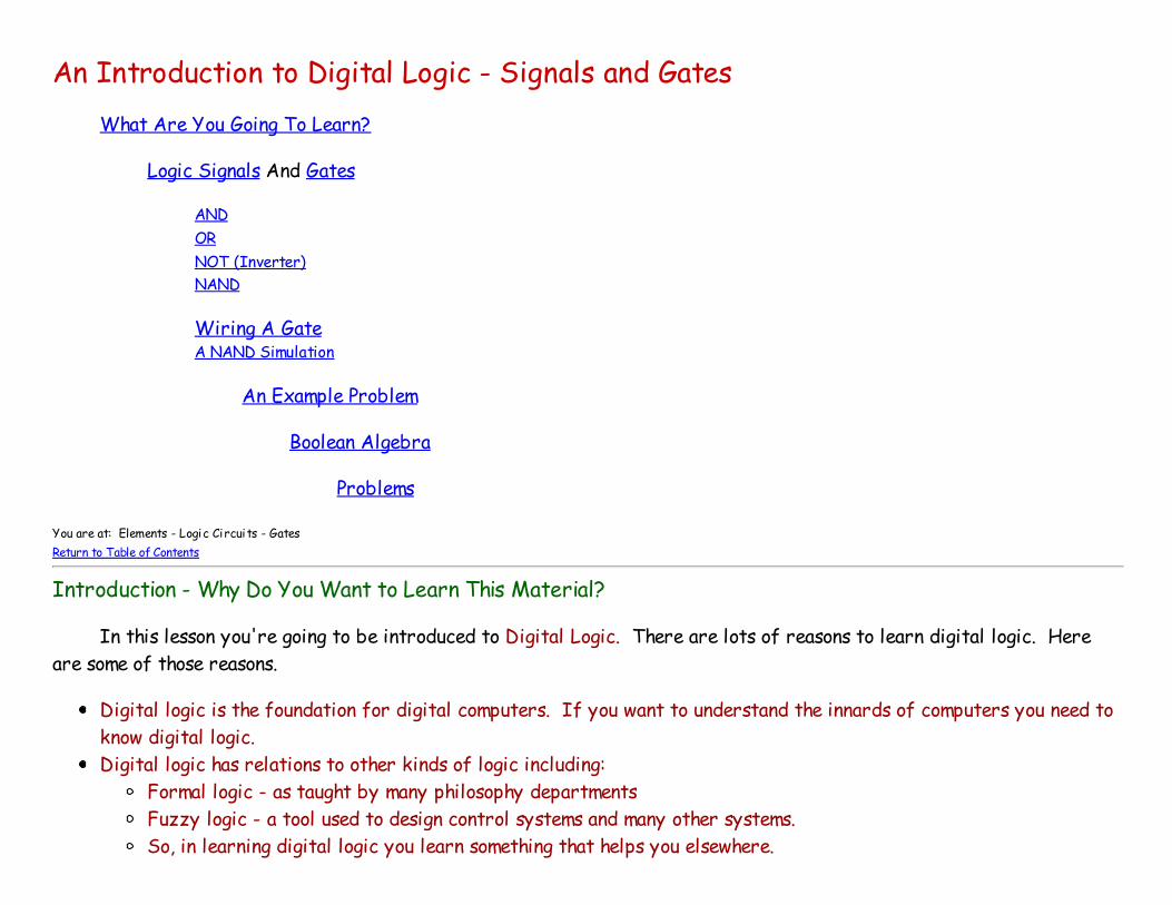
An Introduction to Digital Logic - Signals and Gates
What Are You Going To Learn?
Logic Signals And Gates
AND OR
NOT (Inverter) NAND
Wiring A Gate A NAND Simulation
An Example Problem
Boolean Algebra
Problems
You are at: Elements - Logic Circuits - Gates Return to Table of Contents
Introduction - Why Do You Want to Learn This Material?
In this lesson you're going to be introduced to Digital Logic. There are lots of reasons to learn digital logic. Here
are some of those reasons.
Digital logic is the foundation for digital computers. If you want to understand the innards of computers you need to
know digital logic.
Digital logic has relations to other kinds of logic including:
Formal logic - as taught by many philosophy departments
Fuzzy logic - a tool used to design control systems and many other systems.
So, in learning digital logic you learn something that helps you elsewhere.

For many students, learning digital logic is fun.
What Are You Going to Learn?
There are at least two general areas you need to become familiar with.
First, there's background you need to know - the basics of digital logic - things like zeros and ones (0s and 1s) and
how you can represent signals as sequences of zeroes and ones. Eventually you will want to know how large arrays of
zeroes and ones can be used in computer files to store information in pictures, documents, sounds and even movies and
you'll want to learn about how information can be transmitted, between computers and digital signal sources.
You will also need to know things about digital circuits - gates, flip-flops and memory elements and others - so that
you can eventually design circuits to manipulate digital signals.
Here is a short list of the topics you will learn.
Learn what logic signals look like
Model logic signals
Learn Boolean algebra for logic analysis
Learn about gates that process logic signals
Learn how to design some smaller logic circuits
Learn about flip-flops and memory elements that store logic signals
Objectives For This Lesson
Here's what we are after in this lesson - what you should be able to do.
Given a system that uses logic signals
Be able to specify what the output will be when the input is zero (0) and what the output will be
when the input is one (1).
Given an AND, OR, NAND or NOT gate,
Be able to determine the output of the gate given the input logic signals.
Given a system that requires gates,
Be able to wire a chip correctly, and to check that the chip is functioning properly.
Logic Signals
There are a number of different systems for representing binary information in physical systems. Here are a few.
A voltage signal with zero (0) corresponding to 0 volts and one (1) corresponding to five or three volts.
A sinusoidal signal with zero corresponding to some frequency, and one corresponding to some other frequency.
A current signal with zero corresponding to 4 milliamps and one corresponding to 20 milliamps.
And one last way is to use switches, OPEN for "0" and CLOSED for "1".
(And there are more ways!)
Characteristics of Logic Signals
We should note that all of these signals can and usually will change in time, so that we really are looking at dynamic
situations. However, we will start by looking at these signals as though they were not changing in time.
We will pick a voltage signal as a working example. It can take on two values corresponding to 0 and 1.
We can associate a variable with that logic signal, and we can assign a symbol to represent that variable - like the
symbol A.
Think Binary!
Let's examine a typical situation. You have some sort of device that generates a logic signal.
It could be a telephone that converts your voice signal into a sequence of zeros and ones.
It could be the thermostat on the wall that generates a 1 when the temperature is too low, and a 0 when the
temperature is above the set point temperature.
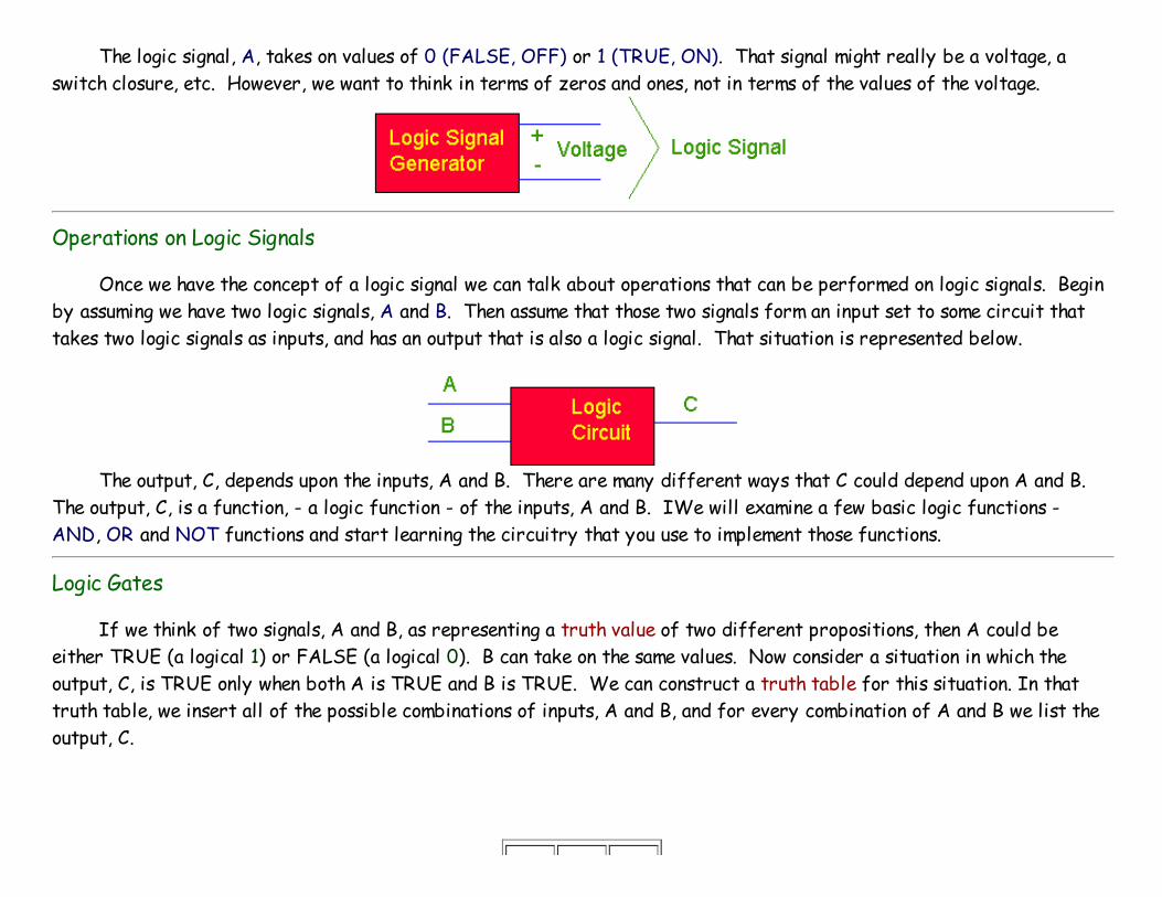
The logic signal, A, takes on values of 0 (FALSE, OFF) or 1 (TRUE, ON). That signal might really be a voltage, a
switch closure, etc. However, we want to think in terms of zeros and ones, not in terms of the values of the voltage.
Operations on Logic Signals
Once we have the concept of a logic signal we can talk about operations that can be performed on logic signals. Begin
by assuming we have two logic signals, A and B. Then assume that those two signals form an input set to some circuit that
takes two logic signals as inputs, and has an output that is also a logic signal. That situation is represented below.
The output, C, depends upon the inputs, A and B. There are many different ways that C could depend upon A and B.
The output, C, is a function, - a logic function - of the inputs, A and B. IWe will examine a few basic logic functions -
AND, OR and NOT functions and start learning the circuitry that you use to implement those functions.
Logic Gates
If we think of two signals, A and B, as representing a truth value of two different propositions, then A could be
either TRUE (a logical 1) or FALSE (a logical 0). B can take on the same values. Now consider a situation in which the
output, C, is TRUE only when both A is TRUE and B is TRUE. We can construct a truth table for this situation. In that
truth table, we insert all of the possible combinations of inputs, A and B, and for every combination of A and B we list the
output, C.
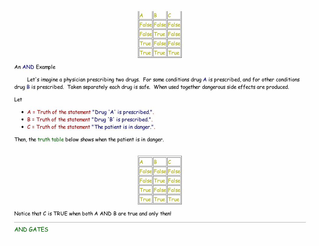
A B C
False False False
False True False
True False False
True True True
An AND Example
Let's imagine a physician prescribing two drugs. For some conditions drug A is prescribed, and for other conditions
drug B is prescribed. Taken separately each drug is safe. When used together dangerous side effects are produced.
Let
A = Truth of the statement "Drug 'A' is prescribed.".
B = Truth of the statement "Drug 'B' is prescribed.".
C = Truth of the statement "The patient is in danger.".
Then, the truth table below shows when the patient is in danger.
A B C
False False False
False True False
True False False
True True True
Notice that C is TRUE when both A AND B are true and only then!
AND GATES
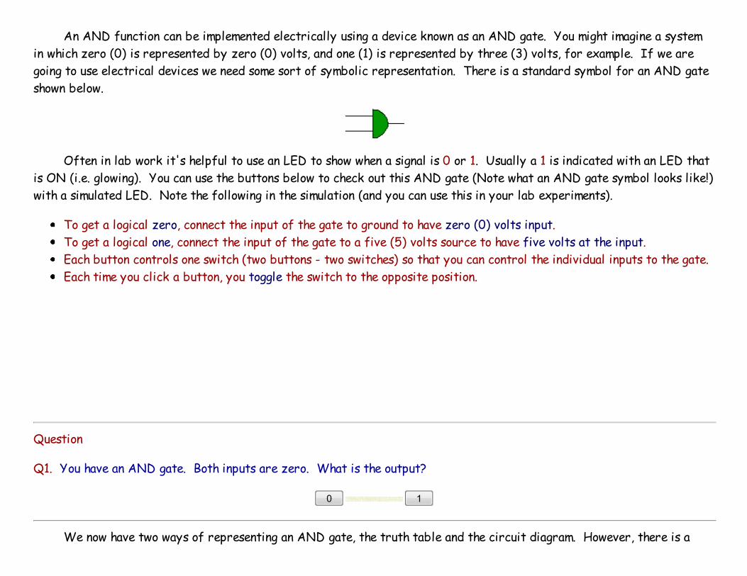
An AND function can be implemented electrically using a device known as an AND gate. You might imagine a system
in which zero (0) is represented by zero (0) volts, and one (1) is represented by three (3) volts, for example. If we are
going to use electrical devices we need some sort of symbolic representation. There is a standard symbol for an AND gate
shown below.
Often in lab work it's helpful to use an LED to show when a signal is 0 or 1. Usually a 1 is indicated with an LED that
is ON (i.e. glowing). You can use the buttons below to check out this AND gate (Note what an AND gate symbol looks like!)
with a simulated LED. Note the following in the simulation (and you can use this in your lab experiments).
To get a logical zero, connect the input of the gate to ground to have zero (0) volts input.
To get a logical one, connect the input of the gate to a five (5) volts source to have five volts at the input.
Each button controls one switch (two buttons - two switches) so that you can control the individual inputs to the gate.
Each time you click a button, you toggle the switch to the opposite position.
Question
Q1. You have an AND gate. Both inputs are zero. What is the output?
0 1
We now have two ways of representing an AND gate, the truth table and the circuit diagram. However, there is a
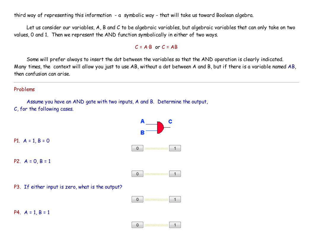
third way of representing this information - a symbolic way - that will take us toward Boolean algebra.
Let us consider our variables, A, B and C to be algebraic variables, but algebraic variables that can only take on two
values, 0 and 1. Then we represent the AND function symbolically in either of two ways.
C = A·B or C = AB
Some will prefer always to insert the dot between the variables so that the AND operation is clearly indicated.
Many times, the context will allow you just to use AB, without a dot between A and B, but if there is a variable named AB,
then confusion can arise.
Problems
Assume you have an AND gate with two inputs, A and B. Determine the output,
C, for the following cases.
P1. A = 1, B = 0
0 1
P2. A = 0, B = 1
0 1
P3. If either input is zero, what is the output?
0 1
P4. A = 1, B = 1
0 1

Once we introduce Boolean variables, we can rethink the concept of a truth table. In the truth table below, if A, B
and C are truth tables and we have an AND gate with A and B as inputs and C as the output, the truth table would look like
this.
A B C
0 0 0
0 1 0
1 0 0
1 1 1
OR Gates
Consider a case where a pressure can be high and a temperature can be high Let's assume we have two sensors that
measure temperature and pressure.. The first sensor has an output, T, that is 1 when a temperature in a boiler is too high,
and 0 otherwise. The second sensor produces an output, P, that is 1 when the pressure is too high, and 0 otherwise. Now,
for the boiler, we have a dangerous situation when either the temperature or the pressure is too high. It only takes one.
Let's construct a truth table for this situation. The output, D, is 1 when danger exists.
T P D
False False False
False True True
True False True
True True True
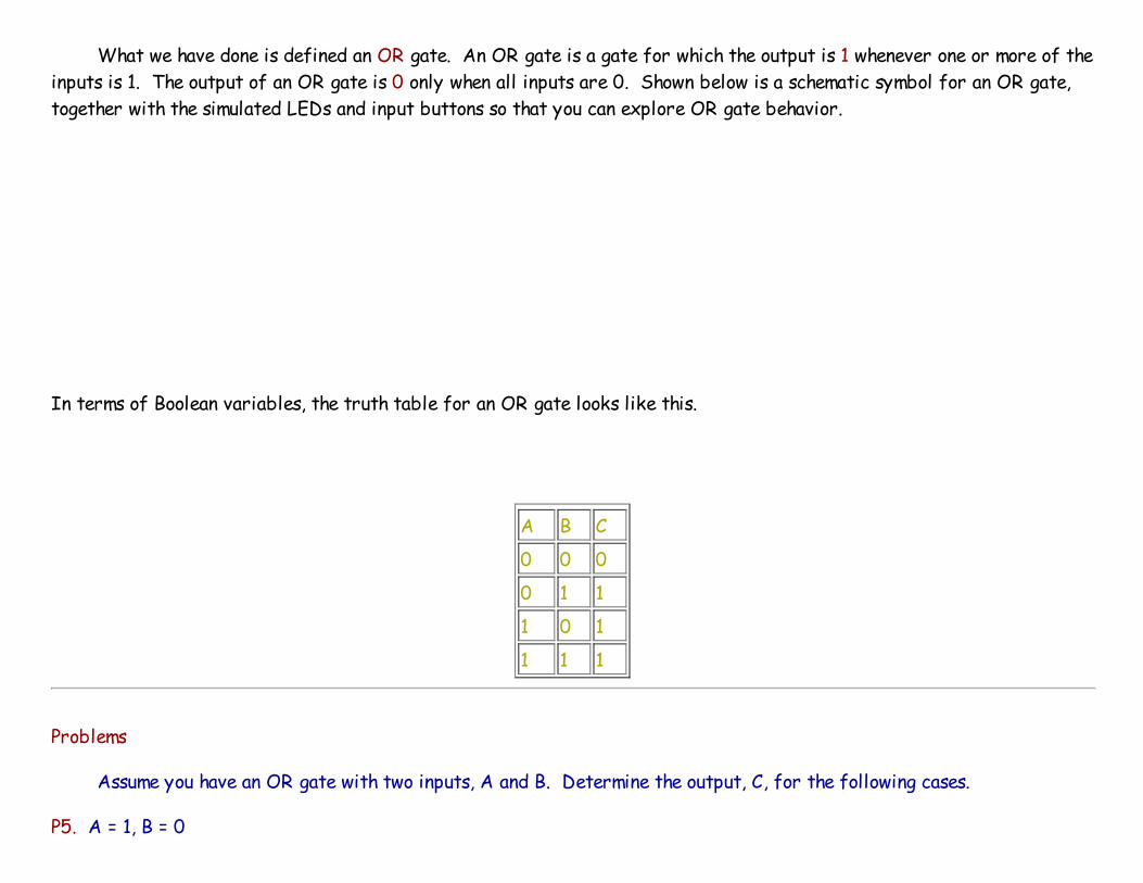
What we have done is defined an OR gate. An OR gate is a gate for which the output is 1 whenever one or more of the
inputs is 1. The output of an OR gate is 0 only when all inputs are 0. Shown below is a schematic symbol for an OR gate,
together with the simulated LEDs and input buttons so that you can explore OR gate behavior.
In terms of Boolean variables, the truth table for an OR gate looks like this.
A B C
0 0 0
0 1 1
1 0 1
1 1 1
Problems
Assume you have an OR gate with two inputs, A and B. Determine the output, C, for the following cases.
P5. A = 1, B = 0

0 1
P6. A = 0, B = 1
0 1
P7. If either input is one, what is the output?
0 1
NOT Gates (Inverters)
A third important logical element is the inverter. An inverter does pretty much what it says. If the input is 0, the
output is 1. Conversely, if the input is 1, the output is 0. The symbol for an inverter is shown below. Again, you can putter
with this inverter with the simulated LEDs. X is the input to the inverter. The output is NOT-X represented as ~1 or:
The truth table for an inverter is pretty simple since there is only one input. Call the input A, and the output C, and
the truth table is:
A C
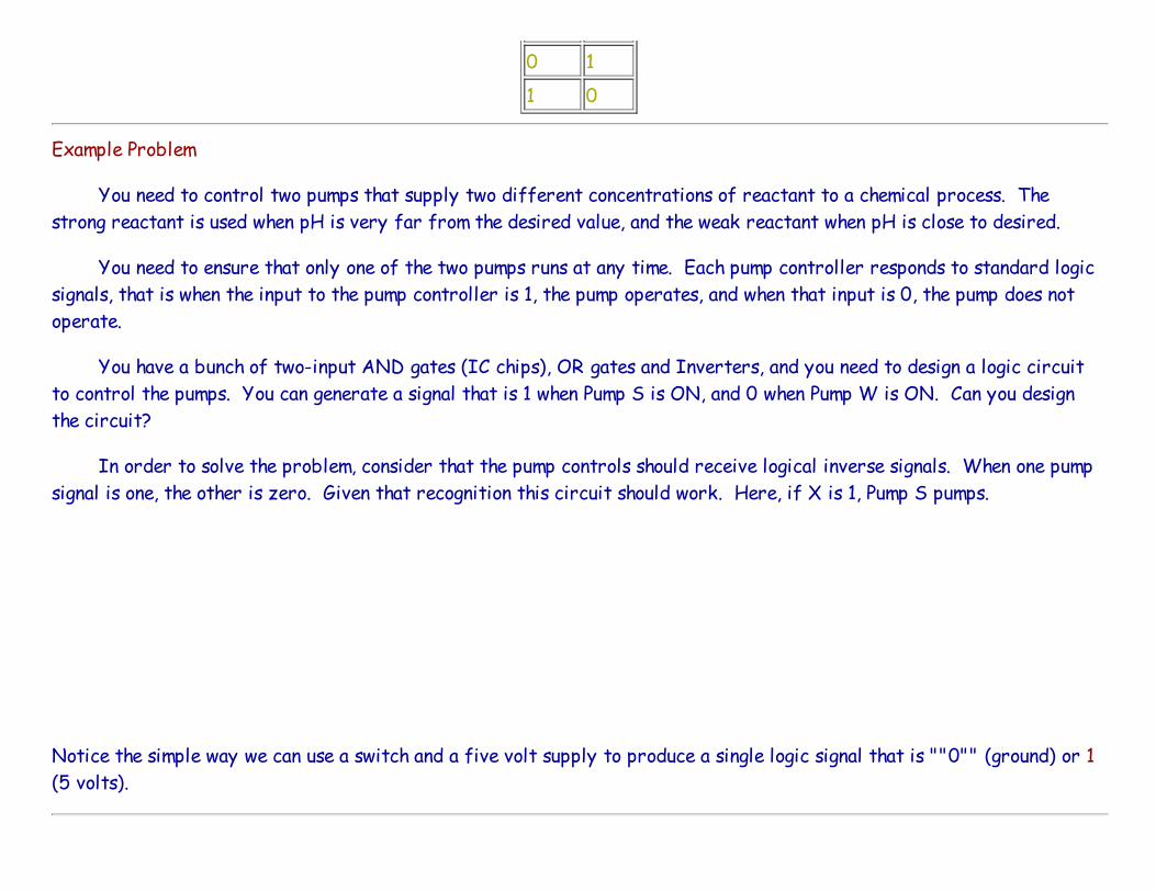
0 1
1 0
Example Problem
You need to control two pumps that supply two different concentrations of reactant to a chemical process. The
strong reactant is used when pH is very far from the desired value, and the weak reactant when pH is close to desired.
You need to ensure that only one of the two pumps runs at any time. Each pump controller responds to standard logic
signals, that is when the input to the pump controller is 1, the pump operates, and when that input is 0, the pump does not
operate.
You have a bunch of two-input AND gates (IC chips), OR gates and Inverters, and you need to design a logic circuit
to control the pumps. You can generate a signal that is 1 when Pump S is ON, and 0 when Pump W is ON. Can you design
the circuit?
In order to solve the problem, consider that the pump controls should receive logical inverse signals. When one pump
signal is one, the other is zero. Given that recognition this circuit should work. Here, if X is 1, Pump S pumps.
Notice the simple way we can use a switch and a five volt supply to produce a single logic signal that is ""0"" (ground) or 1
(5 volts).
NAND Gates
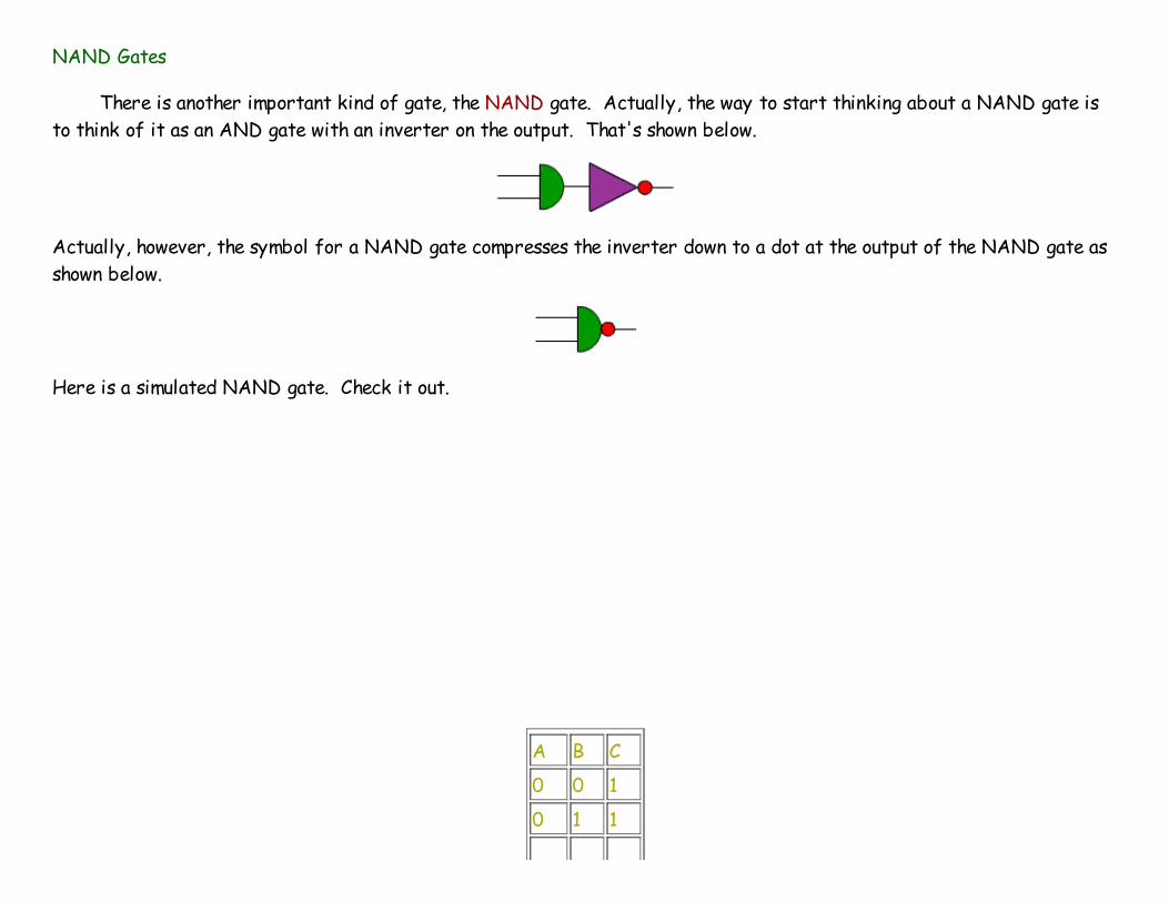
There is another important kind of gate, the NAND gate. Actually, the way to start thinking about a NAND gate is
to think of it as an AND gate with an inverter on the output. That's shown below.
Actually, however, the symbol for a NAND gate compresses the inverter down to a dot at the output of the NAND gate as
shown below.
Here is a simulated NAND gate. Check it out.
A B C
0 0 1
0 1 1

1 0 1
1 1 0
Wiring a Quad-NAND Chip
If you want to use gates, you will need to learn something about their physical characteristics. In this section we'll
walk you through wiring a simple gate circuit using one specific integrated circuit (IC) the 7400 chip. It's a good
introduction to some of the more complex logic chips that you'll probably be using later.
Here's a picture of the 7400 chip in a circuit board. This chip is actually an N74LS00P. The LS tells you that it is
a low power Schottky chip. Every manufacturer will embed the 7400 or 74LS00 in other part numbers.
Notice that this chip has fourteen pins.
If you want to use an IC chip, then you will always need to know the pinout. That's electrical engineering lingo for
describing the way the pins are connected to the internal circuitry of the chip. You need to know where the power supply
is connected and where the gate inputs and outputs are connected. Here's the pinout for a 7400 chip.
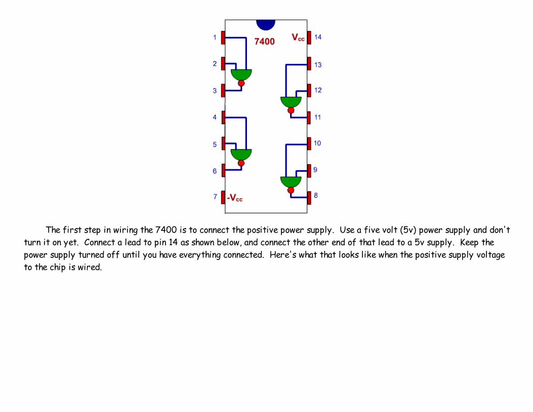
The first step in wiring the 7400 is to connect the positive power supply. Use a five volt (5v) power supply and don't
turn it on yet. Connect a lead to pin 14 as shown below, and connect the other end of that lead to a 5v supply. Keep the
power supply turned off until you have everything connected. Here's what that looks like when the positive supply voltage
to the chip is wired.

The next step in wiring the 7400 is to connect the ground connection. Connect a lead to pin 7 as shown below, and
connect the other end of that lead to ground.
Notice the pattern to this connection. The power to this digital logic chip goes to the corners. Remember, power to
the corners for logic chips.
Now you can connect the two inputs to one of the gates on the chip. You're going to put 5v on either of these inputs
for a 1 and ground the input for a 0. There are two wires in the picture below that connect to pins 1 and 2 on the chip.
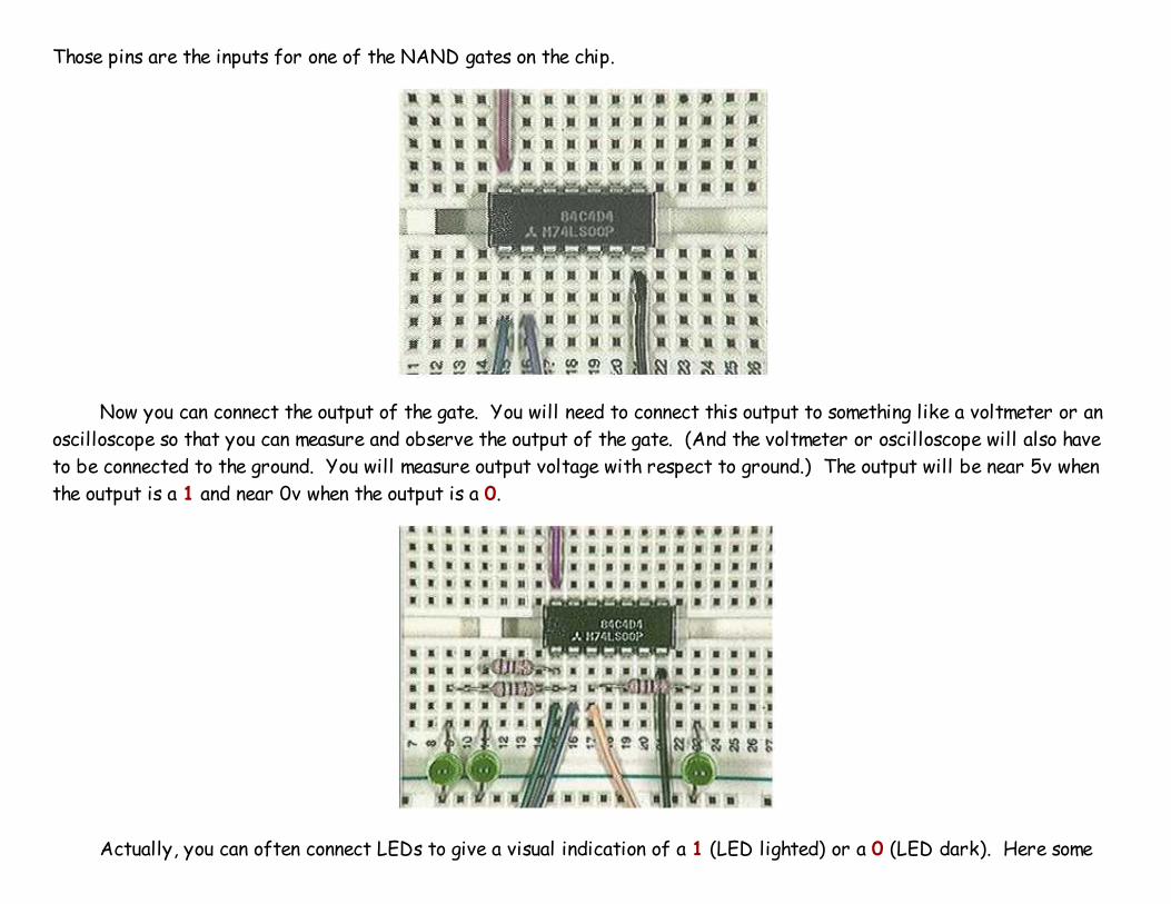
Those pins are the inputs for one of the NAND gates on the chip.
Now you can connect the output of the gate. You will need to connect this output to something like a voltmeter or an
oscilloscope so that you can measure and observe the output of the gate. (And the voltmeter or oscilloscope will also have
to be connected to the ground. You will measure output voltage with respect to ground.) The output will be near 5v when
the output is a 1 and near 0v when the output is a 0.
Actually, you can often connect LEDs to give a visual indication of a 1 (LED lighted) or a 0 (LED dark). Here some
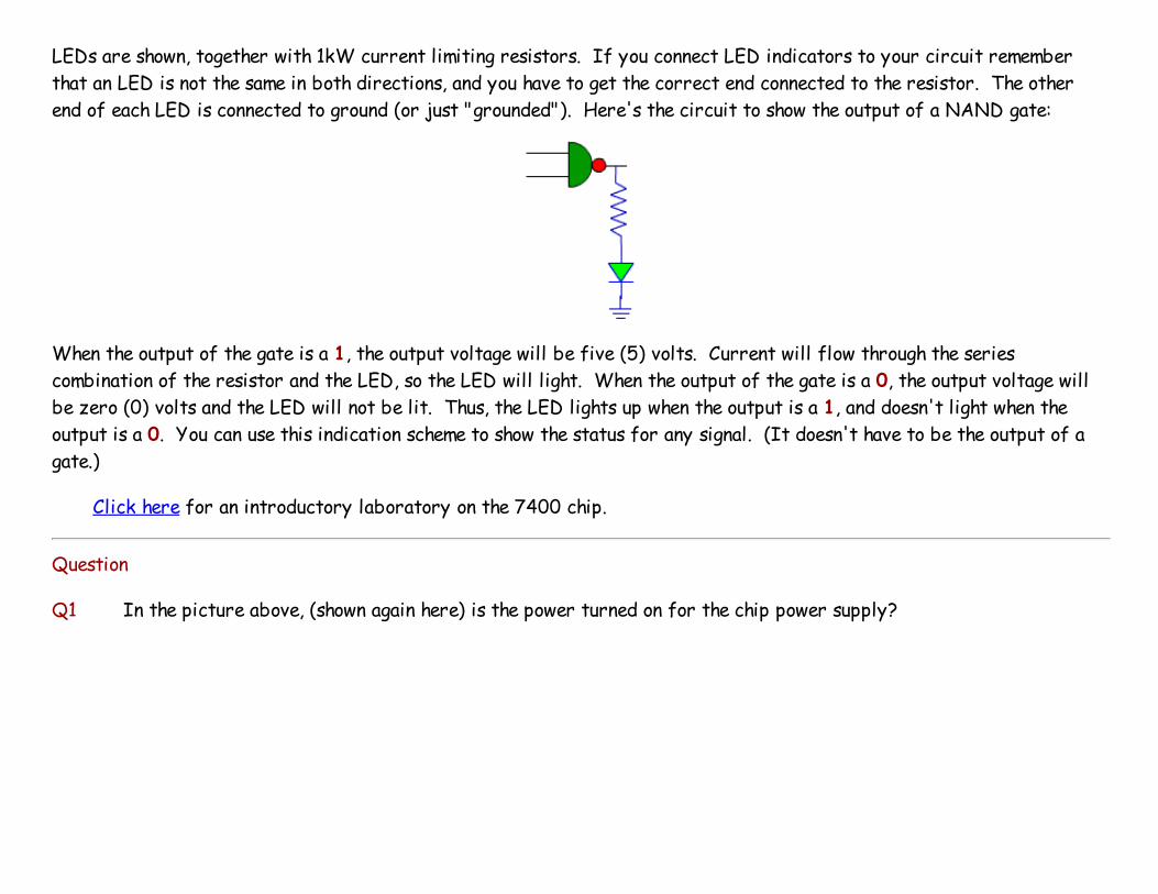
LEDs are shown, together with 1kW current limiting resistors. If you connect LED indicators to your circuit remember
that an LED is not the same in both directions, and you have to get the correct end connected to the resistor. The other
end of each LED is connected to ground (or just "grounded"). Here's the circuit to show the output of a NAND gate:
When the output of the gate is a 1, the output voltage will be five (5) volts. Current will flow through the series
combination of the resistor and the LED, so the LED will light. When the output of the gate is a 0, the output voltage will
be zero (0) volts and the LED will not be lit. Thus, the LED lights up when the output is a 1, and doesn't light when the
output is a 0. You can use this indication scheme to show the status for any signal. (It doesn't have to be the output of a
gate.)
Click here for an introductory laboratory on the 7400 chip.
Question
Q1 In the picture above, (shown again here) is the power turned on for the chip power supply?
Yes No
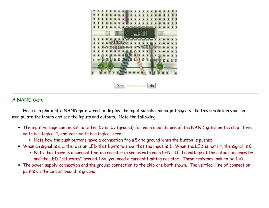
A NAND Gate
Here is a photo of a NAND gate wired to display the input signals and output signals. In this simulation you can
manipulate the inputs and see the inputs and outputs. Note the following.
The input voltage can be set to either 5v or 0v (ground) for each input to one of the NAND gates on the chip. Five
volts is a logical 1, and zero volts is a logical zero.
Note how the push buttons move a connection from 5v to ground when the button is pushed.
When an signal is a 1, there is an LED that lights to show that the input is 1. When the LED is not lit, the signal is 0.
Note that there is a current limiting resistor in series with each LED. If the voltage at the output becomes 5v
and the LED "saturates" around 1.8v, you need a current limiting resistor. These resistors look to be 1kW .
The power supply connection and the ground connection to the chip are both shown. The vertical line of connection
points on the circuit board is ground.
Check out how the circuit works and note all of the connections that you need to make to ensure that the chip works as it is
supposed to work.
Example Problem
Let's reconsider the pump problem. What happens if there are times when you don't want either pump to pump?
Assume you have a digital signal that is 1 when one of the two pumps is to pump, and 0 when neither pump is to pump. For
example, if the pH was very close to desired you wouldn't want to do anything at all so you wouldn't want either pump to
turn on..
You still have the other signal that determines which pump is to pump whenever one of the pumps should pump.
Devise a circuit that will ensure that both pumps are OFF when the Pumpsignal is 0 and that the correct pump pumps
when the Pump signal is 1.
The circuit you devise in this section will be simple enough that you can probably implement it with a few chips
although you will need to look for chips with AND gates and inverters. You should be able to handle that now. Work
through the solution in this lesson and try it out in lab if you can.
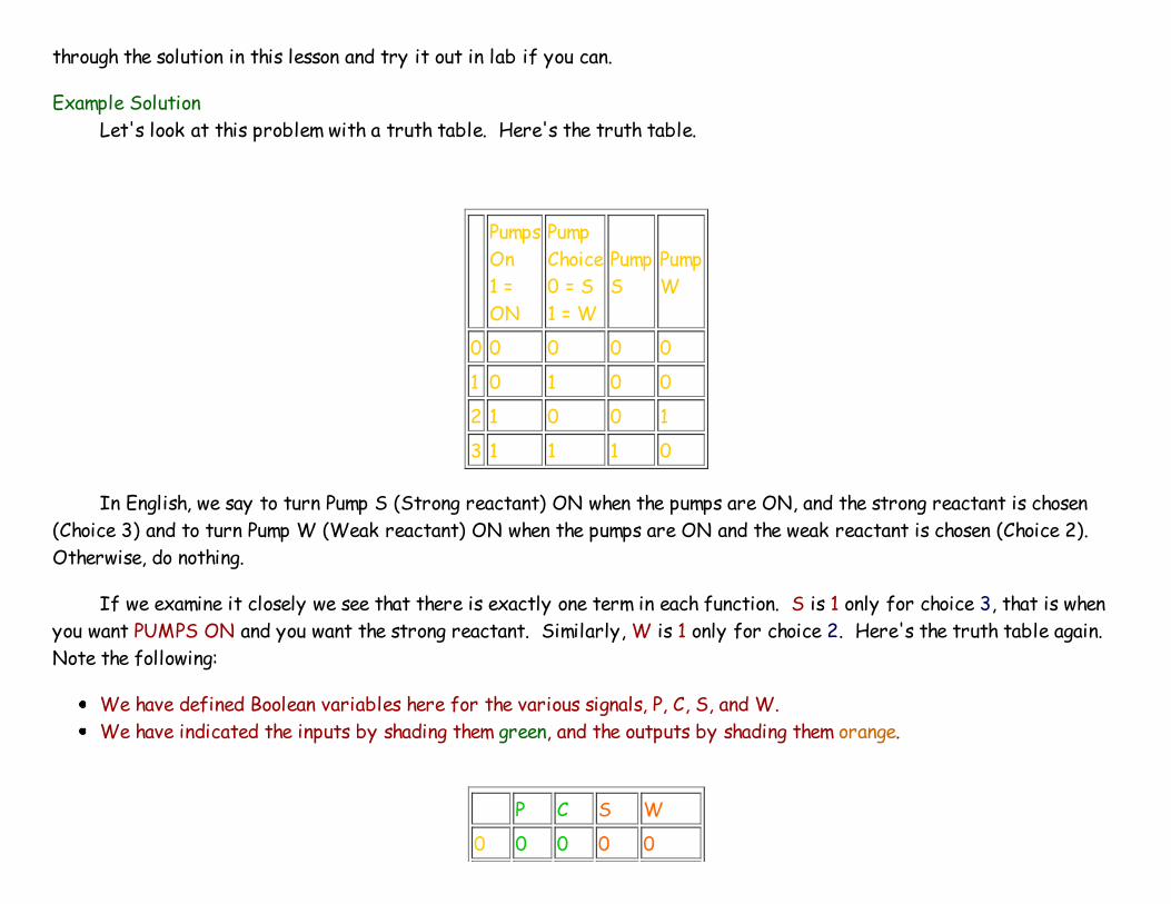
Example Solution
Let's look at this problem with a truth table. Here's the truth table.
Pumps
On
1 =
ON
Pump
Choice
0 = S
1 = W
Pump
S
Pump
W
0 0 0 0 0
1 0 1 0 0
2 1 0 0 1
3 1 1 1 0
In English, we say to turn Pump S (Strong reactant) ON when the pumps are ON, and the strong reactant is chosen
(Choice 3) and to turn Pump W (Weak reactant) ON when the pumps are ON and the weak reactant is chosen (Choice 2).
Otherwise, do nothing.
If we examine it closely we see that there is exactly one term in each function. S is 1 only for choice 3, that is when
you want PUMPS ON and you want the strong reactant. Similarly, W is 1 only for choice 2. Here's the truth table again.
Note the following:
We have defined Boolean variables here for the various signals, P, C, S, and W.
We have indicated the inputs by shading them green, and the outputs by shading them orange.
P C S W
0 0 0 0 0
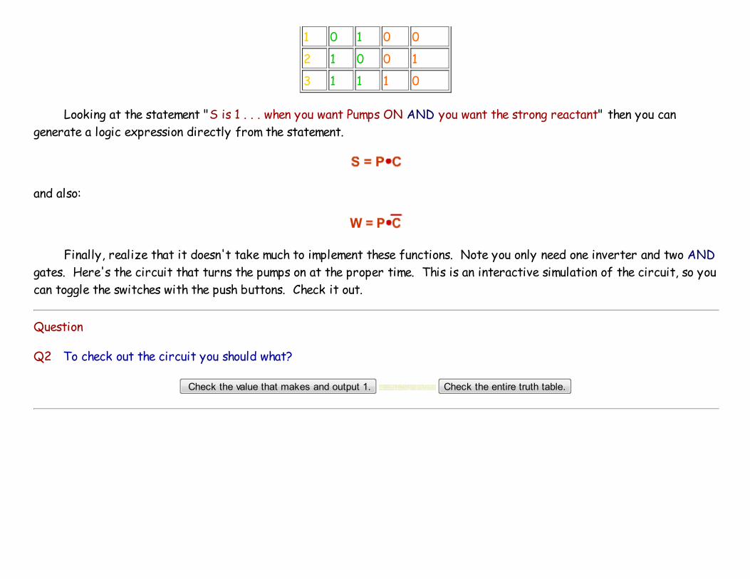
1 0 1 0 0
2 1 0 0 1
3 1 1 1 0
Looking at the statement "S is 1 . . . when you want Pumps ON AND you want the strong reactant" then you can
generate a logic expression directly from the statement.
and also:
Finally, realize that it doesn't take much to implement these functions. Note you only need one inverter and two AND
gates. Here's the circuit that turns the pumps on at the proper time. This is an interactive simulation of the circuit, so you
can toggle the switches with the push buttons. Check it out.
Question
Q2 To check out the circuit you should what?
Check the value that makes and output 1. Check the entire truth table.

A QUICK QUESTION
Within the simulated circuit, determine the part of the circuit that genrates a 1 when the pumps are ON, and a 0 when
they both are OFF.
What If The Problem Isn't So Simple?
Not all functions are as simple as this one, and certainly not all can be implemented with just a few gates. However,
implementing this simple function gives us a clue how to implement more complex functions.
In the next lesson we'll look at a more general method for implementing functions - a method that uses only AND and
OR gates and inverters - but a method which can also be implemented with only NAND gates. We hope that sounds
intriguiging to you and that you are looking forward to the next lesson. Click here to go to the lesson on logic functions.
Boolean Algebra
Clearly at this point we are entering a realm of a different kind of algebra. We have encountered some example
terms in this algebra.

and:
The algebra is unusual because the variables in the algebra (S, P, C and W in the example) can take only two values, 0
and 1. In this section we will examine some of the properties of this algebra, and the implications of what we have already
learned.
There are some simple things we need to establish before we can proceed.
An AND gate has this truth table when the inputs are A and B, and the output is C:
A B C
0 0 0
0 1 0
1 0 0
1 1 1
So, clearly we have:
0·0 = 0, and
1·1 = 1, and
0·1 = 0
Which may be exactly what you expected.
We also need to consider an OR gate.
An OR gate has this truth table when the inputs are A and B, and the output is C:
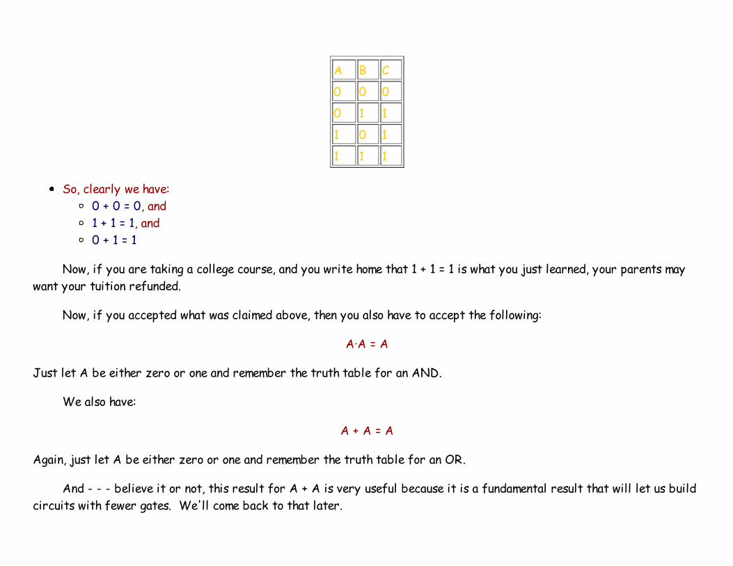
A B C
0 0 0
0 1 1
1 0 1
1 1 1
So, clearly we have:
0 + 0 = 0, and
1 + 1 = 1, and
0 + 1 = 1
Now, if you are taking a college course, and you write home that 1 + 1 = 1 is what you just learned, your parents may
want your tuition refunded.
Now, if you accepted what was claimed above, then you also have to accept the following:
A·A = A
Just let A be either zero or one and remember the truth table for an AND.
We also have:
A + A = A
Again, just let A be either zero or one and remember the truth table for an OR.
And - - - believe it or not, this result for A + A is very useful because it is a fundamental result that will let us build
circuits with fewer gates. We'll come back to that later.
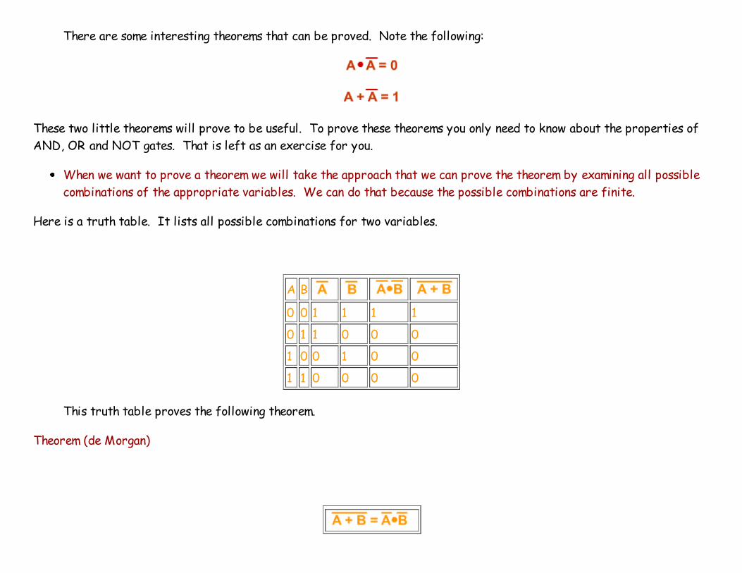
There are some interesting theorems that can be proved. Note the following:
These two little theorems will prove to be useful. To prove these theorems you only need to know about the properties of
AND, OR and NOT gates. That is left as an exercise for you.
When we want to prove a theorem we will take the approach that we can prove the theorem by examining all possible
combinations of the appropriate variables. We can do that because the possible combinations are finite.
Here is a truth table. It lists all possible combinations for two variables.
A B
0 0 1 1 1 1
0 1 1 0 0 0
1 0 0 1 0 0
1 1 0 0 0 0
This truth table proves the following theorem.
Theorem (de Morgan)
Proof
The proof of this theorem is contained in the truth table above which lists every possible combination of A and B, and
shows that this result is true.
One final note. There are some further simple facts that come in useful. Note the following:
and:
Boolean Algebra can be a confusing and misleading business. De Morgan's theorem above seems almost trivial.
However, there is a very interesting consequence of this theorem. Here it is:
If you have a Boolean function that is a sum-of-products form it can be implemented using a two layer circuit with the
first layer composed of AND gates, and the second layer composed of OR gates.
Applying deMorgan's theorem to the function the circuit can be built using the same structure, but replacing every
AND and OR gate with a NAND gate.
First, you need to understand how to expand a function in terms of minterms. Click here to go to that lesson.
Problems
Problem Logic1P01 - Building a Three-Input AND.
Links to Other Lessons on Digital Logic
Gates
Minterms

Karnaugh Maps
Flip-Flops
Counters
Memory Elements
Digital Logic Laboratories
Send your comments on these lessons.