digital logic circuits
DESCRIPTION
Digital logic circuits two marks with answersTRANSCRIPT
UNIT I
1) Given the two binary numbers X = 1010100 and Y = 1000011, perform the
subtraction (a) X
-Y and (b) Y - X using 2’s complements.
a) X = 1010100
2’s complement of Y = + 0111101
--------------
Sum = 10010001
Discard end carry
Answer: X - Y = 0010001
b) Y = 1000011
2’s complement of X = + 0101100
---------------
Sum = 1101111
There is no end carry,
Therefore the answer is Y-X = -(2’s complement of 1101111) = -0010001
2). Given the two binary numbers X = 1010100 and Y = 1000011, perform the
subtraction (a)
X -Y and (b) Y - X using 1’s complements.
a). X - Y = 1010100 - 1000011
X = 1010100
1’s complement of Y = + 0111100
--------------
Sum = 10010000
End -around carry = + 1
--------------
Answer: X - Y = 0010001
b). Y - X = 1000011 - 1010100
Y = 1000011
1’s complement of X = + 0101011
-----------
Sum = + 1101110
There is no end carry.
Therefore the answer is Y - X = -(1’s complement of 1101110) = -0010001
3). What is meant by parity bit?
A parity bit is an extra bit included with a message to make the total number of
1’s either even or odd. Consider the following two characters and their even and odd parity:
With even parity With odd parity
ASCII A = 1000001 01000001 11000001
ASCII T = 1010100 11010100 01010100
In each case we add an extra bit in the left most position of the code to produce
an even number of 1’s in the character for even parity or an odd number of 1’s in the character for odd parity. The parity bit is helpful in detecting errors during the transmission of information from one location to another.
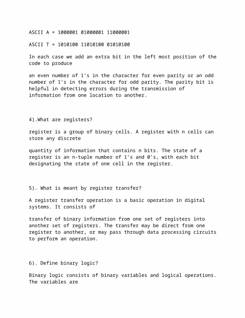
4).What are registers?
register is a group of binary cells. A register with n cells can store any discrete
quantity of information that contains n bits. The state of a register is an n-tuple number of 1’s and 0’s, with each bit designating the state of one cell in the register.
5). What is meant by register transfer?
A register transfer operation is a basic operation in digital systems. It consists of
transfer of binary information from one set of registers into another set of registers. The transfer may be direct from one register to another, or may pass through data processing circuits to perform an operation.
6). Define binary logic?
Binary logic consists of binary variables and logical operations. The variables are
designated by the alphabets such as A, B, C, x, y, z, etc., with each variable
having only two distinct values: 1 and 0. There are three basic logic operations: AND, OR, and NOT.
7). Define logic gates?
Logic gates are electronic circuits that operate on one or more input signals to
produce an output signal. Electrical signals such as voltages or currents exist throughout a digital system in either of two recognizable values. Voltage- operated circuits respond to two separate voltage levels that represent a binary variable equal to logic 1 or logic 0.
8).Define duality property.
Duality property states that every algebraic expression deducible from the
postulates of Boolean algebra remains valid if the operators and identity elements are interchanged. If the dual of an algebraic expression is desired, we simply interchange OR and AND operators and replace 1’s by 0’s and 0’s by 1’s.
9).Find the complement of the functions F1 = x’yz’ + x’y’z and F2 = x(y’z’ +
yz). By applying De Morgan’s theorem as many times as necessary.
F1’ = (x’yz’ + x’y’z)’ = (x’yz’)’(x’y’z)’ = (x + y’ + z)(x + y +z’)
F2’ = [x(y’z’ + yz)]’ = x’ + (y’z’ + yz)’
= x’ + (y’z’)’(yz)’
= x’ + (y + z)(y’ + z’)
10).Find the complements of the functions F1 = x’yz’ + x’y’z and F2 = x(y’z’
+ yz). by taking their duals and complementing each literal.
F1 = x’yz’ + x’y’z
The dual of F1 is (x’ + y + z’)(x’ + y’ + z)
Complementing each literal: (x + y’ + z)(x + y + z’)
F2 = x(y’z’ + yz).
The dual of F2 is x + (y’ + z’)(y + z).
Complement of each literal: x’ + (y + z)(y’ + z’)
11).State De Morgan’s theorem.
De Morgan suggested two theorems that form important part of Boolean algebra.
They are,
1) The complement of a product is equal to the sum of the complements.
(AB)’ = A’ + B’
2) The complement of a sum term is equal to the product of the complements.
(A + B)’ = A’B’
12).Reduce A.A’C
A.A’C = 0.c [A.A’ = 1] = 0
13). Reduce A(A + B)
A(A + B) = AA + AB
= A(1 + B) [1 + B = 1]
= A.
14. Reduce A’B’C’ + A’BC’ + A’BC
A’B’C’ + A’BC’ + A’BC = A’C’(B’ + B) + A’B’C
= A’C’ + A’BC [A + A’ = 1]
= A’(C’ + BC) = A’(C’ + B) [A + A’B = A + B]
15.) Reduce AB + (AC)’ + AB’C(AB + C)
AB + (AC)’ + AB’C(AB + C) = AB + (AC)’ + AAB’BC + AB’CC
= AB + (AC)’ + AB’CC [A.A’ = 0]
= AB + (AC)’ + AB’C [A.A = 1]
= AB + A’ + C’ =AB’C [(AB)’ = A’ + B’]
= A’ + B + C’ + AB’C [A + AB’ = A + B]
= A’ + B’C + B + C’ [A + A’B = A + B]
= A’ + B + C’ + B’C
=A’ + B + C’ + B’
=A’ + C’ + 1
= 1 [A + 1 =1]
16. Simplify the following expression Y = (A + B)(A + C’ )(B’ + C’ )
Y = (A + B)(A + C’ )(B’ + C’ )
= (AA’ + AC +A’B +BC )(B’ + C’) [A.A’ = 0]
= (AC + A’B + BC)(B’ + C’ )
= AB’C + ACC’ + A’BB’ + A’BC’ + BB’C + BCC’
= AB’C + A’BC’
17).Simplify the following using De Morgan’s theorem [((AB)’C)’’ D]’
[((AB)’C)’’ D]’ = ((AB)’C)’’ + D’ [(AB)’ = A’ + B’]
= (AB)’ C + D’
= (A’ + B’ )C + D’
18.Show that (X + Y’ + XY)( X + Y’)(X’Y) = 0
(X + Y’ + XY)( X + Y’)(X’Y) = (X + Y’ + X)(X + Y’ )(X’ + Y) [A + A’B = A + B]
= (X + Y’ )(X + Y’ )(X’Y) [A + A = 1]
= (X + Y’ )(X’Y) [A.A = 1]
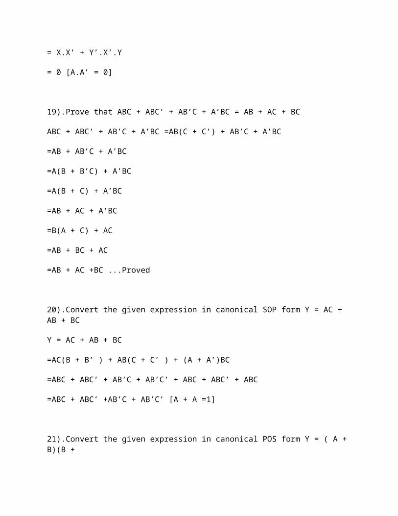
= X.X’ + Y’.X’.Y
= 0 [A.A’ = 0]
19).Prove that ABC + ABC’ + AB’C + A’BC = AB + AC + BC
ABC + ABC’ + AB’C + A’BC =AB(C + C’) + AB’C + A’BC
=AB + AB’C + A’BC
=A(B + B’C) + A’BC
=A(B + C) + A’BC
=AB + AC + A’BC
=B(A + C) + AC
=AB + BC + AC
=AB + AC +BC ...Proved
20).Convert the given expression in canonical SOP form Y = AC + AB + BC
Y = AC + AB + BC
=AC(B + B’ ) + AB(C + C’ ) + (A + A’)BC
=ABC + ABC’ + AB’C + AB’C’ + ABC + ABC’ + ABC
=ABC + ABC’ +AB’C + AB’C’ [A + A =1]
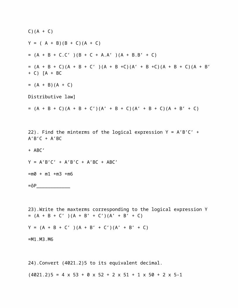
21).Convert the given expression in canonical POS form Y = ( A + B)(B +
C)(A + C)
Y = ( A + B)(B + C)(A + C)
= (A + B + C.C’ )(B + C + A.A’ )(A + B.B’ + C)
= (A + B + C)(A + B + C’ )(A + B +C)(A’ + B +C)(A + B + C)(A + B’ + C) [A + BC
= (A + B)(A + C)
Distributive law]
= (A + B + C)(A + B + C’)(A’ + B + C)(A’ + B + C)(A + B’ + C)
22). Find the minterms of the logical expression Y = A’B’C’ + A’B’C + A’BC
+ ABC’
Y = A’B’C’ + A’B’C + A’BC + ABC’
=m0 + m1 +m3 +m6
=ôP____________
23).Write the maxterms corresponding to the logical expression Y = (A + B + C’ )(A + B’ + C’)(A’ + B’ + C)
Y = (A + B + C’ )(A + B’ + C’)(A’ + B’ + C)
=M1.M3.M6
24).Convert (4021.2)5 to its equivalent decimal.
(4021.2)5 = 4 x 53 + 0 x 52 + 2 x 51 + 1 x 50 + 2 x 5-1
= (511.4)10
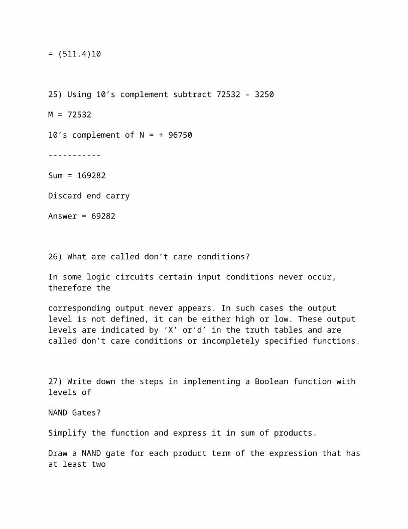
25) Using 10’s complement subtract 72532 - 3250
M = 72532
10’s complement of N = + 96750
-----------
Sum = 169282
Discard end carry
Answer = 69282
26) What are called don’t care conditions?
In some logic circuits certain input conditions never occur, therefore the
corresponding output never appears. In such cases the output level is not defined, it can be either high or low. These output levels are indicated by ‘X’ or‘d’ in the truth tables and are called don’t care conditions or incompletely specified functions.
27) Write down the steps in implementing a Boolean function with levels of
NAND Gates?
Simplify the function and express it in sum of products.
Draw a NAND gate for each product term of the expression that has at least two
literals. The inputs to each NAND gate are the literals of the term. This constitutes a
group of first level gates. Draw a single gate using the AND-invert or the invert-OR graphic symbol in the second level, with inputs coming from outputs of first level gates. A term with a single literal requires an inverter in the first level. How ever if the single literal is complemented, it can be connected directly to an input of the second level NAND gate.
28) Give the general procedure for converting a Boolean expression in to
multilevel NAND diagram?
Draw the AND-OR diagram of the Boolean expression.
Convert all AND gates to NAND gates with AND-invert graphic symbols.
Convert all OR gates to NAND gates with invert-OR graphic symbols.
Check all the bubbles in the same diagram. For every bubble that is not compensated by another circle along the same line, insert an inverter or complement the input literal.
29) What are combinational circuits?
A combinational circuit consists of logic gates whose outputs at any time are
Determined from the present combination of inputs. A combinational circuit performs an operation that can be specified logically by a set of Boolean functions. It consists of input variables, logic gates, and output variables.
30) Give the design procedures for the designing of a combinational circuit.
The procedure involves the following steps,
From the specification of the circuit, determine the required number of inputs and outputs and assign a symbol to each.
Derive the truth table that defines the required relationships between inputs and outputs.
Obtain the simplified Boolean functions for each output as a function of the input variables.
Draw the logic diagram and verify the correctness of the design.
31) Define half adder.
A combinational circuit that performs the addition of two bits is called a half
adder. A half adder needs two binary inputs and two binary outputs. The input variables designate the augend and addend bits; the output variables produce the sum and carry
32) Define full adder?
A combinational circuit that performs the adtion of three bits is a full adder.It consists of three inputs and two outputs.
33) Define binary adder.
A binary adder is a digital circuit that produces the arithmetic sum of two binary
numbers. It can be constructed with full adders constructed in cascade, with the output carry from each full adder connected to the input carry of the next full adder in the chain.
34) What is overflow?
Over flow is a problem in digital computers because the number of bits that hold
The number is finite and a result that contains n + 1 bits cannot be accommodated.
For this reason many computers detect the occurrence of an overflow, and when it occurs a corresponding flip flop is set that can be checked by the user. An overflow condition can be detected by observing the carry into sign bit position and the carry out of the sign bit position. If these two carries are not equal, an overflow has occurred.
35) Define magnitude comparator?
A magnitude comparator is a combinational circuit that compares two numbers, A
and B, and determines their relative magnitudes. The outcome of the comparison is
specified by three binary variables that indicate whether a>b, A = b, or A < B.
36) What are decoders?
A decoder is a combinational circuit that converts binary information from n input
lines to a maximum of 2n unique output lines. If the n bit coded information has unused combinations, The decoder may have fewer than 2n outputs.
37) What are encoders?
An encoder is a digital circuit that performs the inverse operation of a decoder.
An encoder has 2n and n output lines. The output lines generate the binary code
corresponding to the input value.
38) Define priority encoder?
A priority encoder is an encoder circuit that includes the priority function. The
operation of priority encoder is such that if two or more inputs are equal to 1 at the same time, the input having the highest priority will take precedence.
39) Define multiplexer?
A multiplexer is combinational circuit that selects binary information from one of
many input lines and directs it to a single output line. The selection of a particular input line is controlled by a set of selection lines. Normally there are 2n input lines and n selection lines whose bit combinations determine which input is selected.
40) Define binary decoder?
A decoder which has an n- bit binary input code and a one activated output out-of
-2N output code is called binary decoder. A binary decoder is used when it is necessary to activate exactly one of 2N outputs based on an n-bit input value.
16 Marks
1. Obtain the minimum sop using QUINE- McCLUSKY method and verify using K-map F=m0+m2+m4+m8+m9+m10+m11+m12+m13. (16)
2. Reduce the following using tabulation method.
F=m2+m3+m4+m6+m7+m9+m11+m13. (16)
3. Reduce the Boolean function using k-map technique and implement using gates f (w, x, y, z)= _m (0,1,4,8,9,10) which has the don’t cares condition d (w, x, y, z)= _m (2,11). (16)
4. Find the minimum SOP expression using K-map for the function f= _m (7, 9, 10, 11, 12, 13, 14, 15) and realize the minimized function using only NAND gates.(16)
5. a) Expand the following Boolean expression to minterms and maxterms (8)
F= A+BC’+ABD’+ABCD
b).Prove the following (A+B) ((AC)’+C) (B’+AC)’=A’B. (8)
6. a) Design a 2-bit magnitude comparator? (8)
b). Using 8 to 1mux, realize the Boolean function (8)
T=F (w, x, y, z)= _m (0,1,2,4,5,7,8,9,12,13)
7. a) Design an 8421 to gray code converter. (8)
b).Implement the Boolean function using 8:1 mux. (8)
F (A, B, C, D) =A’BD’+ACD+B’CD+A’C’D.
8. a) Explain the operation of 4 to 10 decoder. (8)
b). Implement the following multiple output combinational logic circuit using a
3-to8 decoder.
F1= _m (1, 2, 3, 5, 7)
F2= _m (0, 3, 6)
F3= _m (0, 2, 4, 6) (8)
4. Design a 4-bit adder /subtractor-using logic gates and explains its operation. (16)
5. Construct a combinational circuit to convert BCD to EX-3 code. (16)
6. Design A Full Adder And A Full Subtractor. (16)
UNIT II
1. What are the classification of sequential circuits?
The sequential circuits are classified on the basis of timing of their signals into two
types. They are,
1)Synchronous sequential circuit.
2)Asynchronous sequential circuit.
2. Define Flip flop.
The basic unit for storage is flip flop. A flip-flop maintains its output state either at 1
or 0 until directed by an input signal to change its state.
3.What are the different types of flip-flop?
There are various types of flip flops. Some of them are mentioned below they are,
1. RS flip-flop
2. SR flip-flop
3. D flip-flop
4. JK flip-flop
5. T flip-flop
4.What is the operation of D flip-flop?
In D flip-flop during the occurrence of clock pulse if D=1, the output Q is set and if
D=0, the output is reset.
5. What is the operation of JK flip-flop?
1. When K input is low and J input is high the Q output of flip-flop is set.
2. When K input is high and J input is low the Q output of flip-flop is reset.
3. When both the inputs K and J are low the output does not change
4. When both the inputs K and J are high it is possible to set or reset the flip-flop (ie) the output toggle on the next positive clock edge.
6. What is the operation of T flip-flop?
T flip-flop is also known as Toggle flip-flop.
1. When T=0 there is no change in the output.
2. When T=1 the output switch to the complement state (ie) the output toggles.
7. Define race around condition.
In JK flip-flop output is fed back to the input. Therefore change in the output results change in the input. Due to this in the positive half of the clock pulse if both J and K are high then output toggles continuously. This condition is called ‘race around condition’.
8. What is edge-triggered flip-flop?
The problem of race around condition can solved by edge triggering flip flop. The term edge triggering means that the flip-flop changes state either at the positive edge or negative edge of the clock pulse and it is sensitive to its inputs only at this transition of the clock.
9. What is a master-slave flip-flop?
A master-slave flip-flop consists of two flip-flops where one circuit serves as a master and the other as a slave.
10.Define rise time.
The time required to change the voltage level from 10% to 90% is known as rise time(tr).
11.Define fall time.
The time required to change the voltage level from 90% to 10% is known as fall
time(tf).
12.Define skew and clock skew.
The phase shift between the rectangular clock waveforms is referred to as skew and the time delay between the two clock pulses is called clock skew.
13.Define setup time.
The setup time is the minimum time required to maintain a constant voltage levels at the excitation inputs of the flip-flop device prior to the triggering edge of the clock pulse in order for the levels to be reliably clocked into the flip flop. It is denoted as tsetup.
14. Define hold time.
The hold time is the minimum time for which the voltage levels at the excitation inputs must remain constant after the triggering edge of the clock pulse in order for the levels to be reliably clocked into the flip flop. It is denoted as thold .
15. Define propagation delay.
A propagation delay is the time required to change the output after the application of the input.
16.Define registers.
A register is a group of flip-flops flip-flop can store one bit information. So an n-bit register has a group of n flip-flops and is capable of storing any binary information/number containing n-bits.
17.Define shift registers.
The binary information in a register can be moved from stage to stage within the register or into or out of the register upon application of clock pulses. This type of bit movement or shifting is essential for certain arithmetic and logic operations used in microprocessors. This gives rise to group of registers called shift registers.
18.What are the different types of shift type?
There are five types. They are,
_Serial In Serial Out Shift Register
_Serial In Parallel Out Shift Register
_Parallel In Serial Out Shift Register
_Parallel In Parallel Out Shift Register
_Bi-directional Shift Register
19.Explain the flip-flop excitation tables for RS FF.
In RS flip-flop there are four possible transitions from the present state to the
next state. They are,
0 0 transition: This can happen either when R=S=0 or when R=1 and S=0.
0 1 transition: This can happen only when S=1 and R=0.
1 0 transition: This can happen only when S=0 and R=1.
1 1 transition: This can happen either when S=1 and R=0 or S=0 and R=0.
20. Define sequential circuit?
In sequential circuits the output variables dependent not only on the present input variables but they also depend up on the past history of these input variables.
21.Give the comparison between combinational circuits and sequential circuits.
Combinational circuits Sequential circuits
Memory unit is not required Memory unity is required
Parallel adder is a combinational circuit Serial adder is a sequential circuit
22. What do you mean by present state?
The information stored in the memory elements at any given time defines the present state of the sequential circuit.
23. What do you mean by next state?
The present state and the external inputs determine the outputs and the next state of the sequential circuit.
24.State the types of sequential circuits?
1. Synchronous sequential circuits
2. Asynchronous sequential circuits
25. Define synchronous sequential circuit
In synchronous sequential circuits, signals can affect the memory elements only at discrete instant of time.
Enter or copy paste question here
1. Obtain the minimum sop using QUINE- McCLUSKY method and verify using K-map F=m0+m2+m4+m8+m9+m10+m11+m12+m13. (16)
2. Reduce the following using tabulation method.
F=m2+m3+m4+m6+m7+m9+m11+m13. (16)
3. Reduce the Boolean function using k-map technique and implement using gates f (w, x, y, z)= _m (0,1,4,8,9,10) which has the don’t cares condition d (w, x, y, z)= _m (2,11). (16)
4. Find the minimum SOP expression using K-map for the function f= _m (7, 9, 10, 11, 12, 13, 14, 15) and realize the minimized function using only NAND gates.(16)
5. a) Expand the following Boolean expression to minterms and maxterms (8)
F= A+BC’+ABD’+ABCD
b).Prove the following (A+B) ((AC)’+C) (B’+AC)’=A’B. (8)
6. a) Design a 2-bit magnitude comparator? (8)
b). Using 8 to 1mux, realize the Boolean function (8)
T=F (w, x, y, z)= _m (0,1,2,4,5,7,8,9,12,13)
7. a) Design an 8421 to gray code converter. (8)
b).Implement the Boolean function using 8:1 mux. (8)
F (A, B, C, D) =A’BD’+ACD+B’CD+A’C’D.
8. a) Explain the operation of 4 to 10 decoder. (8)
b). Implement the following multiple output combinational logic circuit using a
3-to8 decoder.
F1= _m (1, 2, 3, 5, 7)
F2= _m (0, 3, 6)
F3= _m (0, 2, 4, 6) (8)
4. Design a 4-bit adder /subtractor-using logic gates and explains its operation. (16)
5. Construct a combinational circuit to convert BCD to EX-3 code. (16)
6. Design A Full Adder And A Full Subtractor. (16)
UNIT III
1. What are the classification of sequential circuits?
The sequential circuits are classified on the basis of timing of their signals into two
types. They are,
1)Synchronous sequential circuit.
2)Asynchronous sequential circuit.
2. Define Flip flop.
The basic unit for storage is flip flop. A flip-flop maintains its output state either at 1
or 0 until directed by an input signal to change its state.
3.What are the different types of flip-flop?
There are various types of flip flops. Some of them are mentioned below they are,
1. RS flip-flop2. SR flip-flop3. D flip-flop4. JK flip-flop5. T flip-flop
4.What is the operation of D flip-flop?
In D flip-flop during the occurrence of clock pulse if D=1, the output Q is set and if
D=0, the output is reset.
5. What is the operation of JK flip-flop?
1. When K input is low and J input is high the Q output of flip-flop is set.2. When K input is high and J input is low the Q output of flip-flop is reset.3. When both the inputs K and J are low the output does not change4. When both the inputs K and J are high it is possible to set or reset the flip-flop (ie) the
output toggle on the next positive clock edge.
6. What is the operation of T flip-flop?
T flip-flop is also known as Toggle flip-flop.
1. When T=0 there is no change in the output.2. When T=1 the output switch to the complement state (ie) the output toggles.
7. Define race around condition.
In JK flip-flop output is fed back to the input. Therefore change in the output results change in the input. Due to this in the positive half of the clock pulse if both J and K are high then output toggles continuously. This condition is called ‘race around condition’.
8. What is edge-triggered flip-flop?
The problem of race around condition can solved by edge triggering flip flop. The term edge triggering means that the flip-flop changes state either at the positive edge or negative edge of the clock pulse and it is sensitive to its inputs only at this transition of the clock.
9. What is a master-slave flip-flop?
A master-slave flip-flop consists of two flip-flops where one circuit serves as a master and the other as a slave.
10.Define rise time.
The time required to change the voltage level from 10% to 90% is known as rise time(tr).
11.Define fall time.
The time required to change the voltage level from 90% to 10% is known as fall
time(tf).
12.Define skew and clock skew.
The phase shift between the rectangular clock waveforms is referred to as skew and the time delay between the two clock pulses is called clock skew.
13.Define setup time.
The setup time is the minimum time required to maintain a constant voltage levels at the excitation inputs of the flip-flop device prior to the triggering edge of the clock pulse in order for the levels to be reliably clocked into the flip flop. It is denoted as tsetup.
14. Define hold time.
The hold time is the minimum time for which the voltage levels at the excitation inputs must remain constant after the triggering edge of the clock pulse in order for the levels to be reliably clocked into the flip flop. It is denoted as thold .
15. Define propagation delay.
A propagation delay is the time required to change the output after the application of the input.
16.Define registers.
A register is a group of flip-flops flip-flop can store one bit information. So an n-bit register has a group of n flip-flops and is capable of storing any binary information/number containing n-bits.
17.Define shift registers.
The binary information in a register can be moved from stage to stage within the register or into or out of the register upon application of clock pulses. This type of bit movement or shifting is essential for certain arithmetic and logic operations used in microprocessors. This gives rise to group of registers called shift registers.
18.What are the different types of shift type?
There are five types. They are,
_Serial In Serial Out Shift Register
_Serial In Parallel Out Shift Register
_Parallel In Serial Out Shift Register
_Parallel In Parallel Out Shift Register
_Bi-directional Shift Register
19.Explain the flip-flop excitation tables for RS FF.
In RS flip-flop there are four possible transitions from the present state to the
next state. They are,
0 0 transition: This can happen either when R=S=0 or when R=1 and S=0.
0 1 transition: This can happen only when S=1 and R=0.
1 0 transition: This can happen only when S=0 and R=1.
1 1 transition: This can happen either when S=1 and R=0 or S=0 and R=0.
20. Define sequential circuit?
In sequential circuits the output variables dependent not only on the present input variables but they also depend up on the past history of these input variables.
21.Give the comparison between combinational circuits and sequential circuits.
Combinational circuits Sequential circuits
Memory unit is not required Memory unity is required
Parallel adder is a combinational circuit Serial adder is a sequential circuit
22. What do you mean by present state?
The information stored in the memory elements at any given time defines the present state of the sequential circuit.
23. What do you mean by next state?
The present state and the external inputs determine the outputs and the next state of the sequential circuit.
24.State the types of sequential circuits?
1. Synchronous sequential circuits
2. Asynchronous sequential circuits
25. Define synchronous sequential circuit
In synchronous sequential circuits, signals can affect the memory elements only at discrete instant of time.
16 Marks
1. Design an asynchronous sequential circuit that has 2 inputs x2 and x1, and one output z. the output is to remain a 0 as long as a 0.the first change in x2 that occurs while x1 is a1 will cause z to be a1. z is to remain a1 until x1 returns to 0. Construct a state diagram and flow table. Determine the output equations. (16)
2. Draw the fundamental mode and pulse mode asynchronous sequential circuits
and explain in detail. (16)
3. Minimize the following state table. (16)
NS,X
X
P.S 0 1
A A, 0 D, 0
B C, 1 D, 0
C B, 0 A, 1
D D,1 A,1
E D,1 A,1
F D,0 A,0
G D,1 A,1
H D,1 C,1
4. Obtain the primitive flow table for an asynchronous circuit that has 2 input’s x, y and output z. an output z=1, is to occur only during the input state xy=01 and then if and only if the input state xy=01 is preceded by the input sequence xy=01, 00, 10,00,10,00 (16)
5. Design a circuit with input a and b to give an output z=1 when AB =11 but only if A becomes 1 before B, by drawing total state diagram, primitive flow table and output map in which transient state is included. (16)
UNIT IV
1.Give the classification of logic families
Bipolar Unipolar
Saturated Non Saturated PMOS
NMOS
CMOS
RTL Schottky TTL
ECL DTL
I I L
TTL
2. Which gates are called as the universal gates? What are its advantages?
The NAND and NOR gates are called as the universal gates. These gates are used to perform any type of logic application.
3.Classify the logic family by operation?
The Bipolar logic family is classified into
Saturated logic
Unsaturated logic.
The RTL, DTL, TTL, I2L, HTL logic comes under the saturated logic family.
The Schottky TTL, and ECL logic comes under the unsaturated logic family.
4.State the classifications of FET devices.
FET is classified as
1. Junction Field Effect Transistor (JFET)
2. Metal oxide semiconductor family (MOS).
5.Mention the classification of saturated bipolar logic families.
The bipolar logic family is classified as follows:
RTL- Resistor Transistor Logic
DTL- Diode Transistor logic
I2L- Integrated Injection Logic
TTL- Transistor Transistor Logic
ECL- Emitter Coupled Logic
6. Mention the important characteristics of digital IC’s?
Fan out
Power dissipation
Propagation Delay
Noise Margin
Fan In
Operating temperature
Power supply requirements
7. Define Fan-out?
Fan out specifies the number of standard loads that the output of the gate can drive with out impairment of its normal operation.
8. Define power dissipation?
Power dissipation is measure of power consumed by the gate when fully driven by all its inputs.
9. What is propagation delay?
Propagation delay is the average transition delay time for the signal to propagate from input to output when the signals change in value. It is expressed in ns.
10. Define noise margin?
It is the maximum noise voltage added to an input signal of a digital circuit that does
not cause an undesirable change in the circuit output. It is expressed in volts.
11. Define fan in?
Fan in is the number of inputs connected to the gate without any degradation in the
voltage level.
12. What is Operating temperature?
All the gates or semiconductor devices are temperature sensitive in nature. The temperature in which the performance of the IC is effective is called as operating temperature. Operating temperature of the IC vary from 00 C to 700 c.
13.What is High Threshold Logic?
Some digital circuits operate in environments, which produce very high noise signals. For operation in such surroundings there is available a type of DTL gate which possesses a high threshold to noise immunity. This type of gate is called HTL logic or High Threshold Logic.
14. What are the types of TTL logic?
1. Open collector output
2. Totem-Pole Output
3. Tri-state output.
15. What is depletion mode operation MOS?
If the channel is initially doped lightly with p-type impurity a conducting channel exists at zero gate voltage and the device is said to operate in depletion mode.
16. What is enhancement mode operation of MOS?
If the region beneath the gate is left initially uncharged the gate field must induce a channel before current can flow. Thus the gate voltage enhances the channel current and such a device is said to operate in the enhancement mode.
17. Mention the characteristics of MOS transistor?
1. The n- channel MOS conducts when its gate- to- source voltage is positive.
2. The p- channel MOS conducts when its gate- to- source voltage is negative
3. Either type of device is turned of if its gate- to- source voltage is zero.
18. How schottky transistors are formed and state its use?
A schottky diode is formed by the combination of metal and semiconductor. The presence of schottky diode between the base and the collector prevents the transistor from going into saturation. The resulting transistor is called as schottky transistor. The use of schottky transistor in TTL decreases the propagation delay without a sacrifice of power dissipation.
19. List the different versions of TTL
1.TTL (Std.TTL) 2.LTTL (Low Power TTL)
3.HTTL (High Speed TTL) 4.STTL (Schottky TTL)
5.LSTTL (Low power Schottky TTL)
20. Why totem pole outputs cannot be connected together.
Totem pole outputs cannot be connected together because such a connection might produce excessive current and may result in damage to the devices.
21. State advantages and disadvantages of TTL
Adv:
Easily compatible with other ICs
Low output impedance
Disadv:
Wired output capability is possible only with tristate and open collector types
Special circuits in Circuit layout and system design are required.
22. When does the noise margin allow digital circuits to function properly.
When noise voltages are within the limits of VNA(High State Noise Margin) and VNK for a particular logic family.
23. What happens to output when a tristate circuit is selected for high impedance. Output is disconnected from rest of the circuits by internal circuitry.
24. What is 14000 series.
It is the oldest and standard CMOS family. The devices are not pin compatible or electrically compatible with any TTL Series.
25. Explain PROM.
_ PROM (Programmable Read Only Memory)
It allows user to store data or program. PROMs use the fuses with material like nichrome and polycrystalline. The user can blow these fuses by passing around 20 to 50 mA of current for the period 5 to 20μs.The blowing of fuses is called programming of ROM. The PROMs are one time programmable. Once programmed, the information is stored permanent.
26. Explain EPROM.
EPROM(Erasable Programmable Read Only Memory)
EPROM use MOS circuitry. They store 1’s and 0’s as a packet of charge in a buried layer of the IC chip. We can erase the stored data in the EPROMs by exposing the chip to ultraviolet light via its quartz window for 15 to 20 minutes. It is not possible to erase selective information. The chip can be reprogrammed.
27. Explain EEPROM.
EEPROM(Electrically Erasable Programmable Read Only Memory)
EEPROM also use MOS circuitry. Data is stored as charge or no charge on an insulated layer or an insulated floating gate in the device. EEPROM allows selective erasing at the register level rather than erasing all the information since the information can be changed by using electrical signals.
28. What is RAM?
Random Access Memory. Read and write operations can be carried out.
29. What is programmable logic array? How it differs from ROM?
In some cases the number of don’t care conditions is excessive, it is more economical to use a second type of LSI component called a PLA. A PLA is similar to a ROM in concept; however it does not provide full decoding of the variables and does not generates all the minterms as in the ROM.
30.What is mask - programmable?
With a mask programmable PLA, the user must submit a PLA program table to the
manufacturer.
31. What is field programmable logic array?
The second type of PLA is called a field programmable logic array. The user by means of certain recommended procedures can program the EPLA.
32. List the major differences between PLA and PAL
PLA: PAL
Both AND and OR arrays AND arrays are programmable OR are programmable and Complex arrays are fixed
Costlier than PAL Cheaper and Simpler
33. Define PLD.
Programmable Logic Devices consist of a large array of AND gates and OR gates that can be programmed to achieve specific logic functions.
34. Give the classification of PLDs.
PLDs are classified as PROM(Programmable Read Only Memory), Programmable
Logic Array(PLA), Programmable Array Logic (PAL), and Generic Array Logic(GAL)
35. Define PROM.
PROM is Programmable Read Only Memory. It consists of a set of fixed AND gates
connected to a decoder and a programmable OR array.
36. Define PLA
PLA is Programmable Logic Array(PLA). The PLA is a PLD that consists of a programmable AND array and a programmable OR array.
37. Define PAL
PAL is Programmable Array Logic. PAL consists of a programmable AND array and a fixed OR array with output logic.
38. Why was PAL developed ?
It is a PLD that was developed to overcome certain disadvantages of PLA, such as longer delays due to additional fusible links that result from using two programmable arrays and more circuit complexity.
39. Why the input variables to a PAL are buffered
The input variables to a PAL are buffered to prevent loading by the large number of
AND gate inputs to which available or its complement can be connected.
40. What does PAL 10L8 specify ?
PAL - Programmable Logic Array
10 - Ten inputs
L - Active LOW Ouput
8 - Eight Outputs
41.Give the comparison between PROM and PLA.
PROM PLA
1. And array is fixed and OR Both AND and OR arrays are
array is programmable. Programmable.
2. Cheaper and simple to use. Costliest and complex than
PROMS.
The sequential circuits are classified on the basis of timing of their signals into two
types. They are,
1)Synchronous sequential circuit.
2)Asynchronous sequential circuit.
2. Define Flip flop.
The basic unit for storage is flip flop. A flip-flop maintains its output state either at 1
or 0 until directed by an input signal to change its state.
3.What are the different types of flip-flop?
There are various types of flip flops. Some of them are mentioned below they are,
1. RS flip-flop2. SR flip-flop3. D flip-flop4. JK flip-flop5. T flip-flop
4.What is the operation of D flip-flop?
In D flip-flop during the occurrence of clock pulse if D=1, the output Q is set and if
D=0, the output is reset.
5. What is the operation of JK flip-flop?
1. When K input is low and J input is high the Q output of flip-flop is set.2. When K input is high and J input is low the Q output of flip-flop is reset.3. When both the inputs K and J are low the output does not change4. When both the inputs K and J are high it is possible to set or reset the flip-flop (ie) the
output toggle on the next positive clock edge.
6. What is the operation of T flip-flop?
T flip-flop is also known as Toggle flip-flop.
1. When T=0 there is no change in the output.2. When T=1 the output switch to the complement state (ie) the output toggles.
7. Define race around condition.
In JK flip-flop output is fed back to the input. Therefore change in the output results change in the input. Due to this in the positive half of the clock pulse if both J and K are high then output toggles continuously. This condition is called ‘race around condition’.
8. What is edge-triggered flip-flop?
The problem of race around condition can solved by edge triggering flip flop. The term edge triggering means that the flip-flop changes state either at the positive edge or negative edge of the clock pulse and it is sensitive to its inputs only at this transition of the clock.
9. What is a master-slave flip-flop?
A master-slave flip-flop consists of two flip-flops where one circuit serves as a master and the other as a slave.
10.Define rise time.
The time required to change the voltage level from 10% to 90% is known as rise time(tr).
11.Define fall time.
The time required to change the voltage level from 90% to 10% is known as fall
time(tf).
12.Define skew and clock skew.
The phase shift between the rectangular clock waveforms is referred to as skew and the time delay between the two clock pulses is called clock skew.
13.Define setup time.
The setup time is the minimum time required to maintain a constant voltage levels at the excitation inputs of the flip-flop device prior to the triggering edge of the clock pulse in order for the levels to be reliably clocked into the flip flop. It is denoted as tsetup.
14. Define hold time.
The hold time is the minimum time for which the voltage levels at the excitation inputs must remain constant after the triggering edge of the clock pulse in order for the levels to be reliably clocked into the flip flop. It is denoted as thold .
15. Define propagation delay.
A propagation delay is the time required to change the output after the applic ation of the input.
16.Define registers.
A register is a group of flip-flops flip-flop can store one bit information. So an n-bit register has a group of n flip-flops and is capable of storing any binary information/number containing n-bits.
17.Define shift registers.
The binary information in a register can be moved from stage to stage within the register or into or out of the register upon application of clock pulses. This type of bit movement or shifting is essential for certain arithmetic and logic operations used in microprocessors. This gives rise to group of registers called shift registers.
18.What are the different types of shift type?
There are five types. They are,
_Serial In Serial Out Shift Register
_Serial In Parallel Out Shift Register
_Parallel In Serial Out Shift Register
_Parallel In Parallel Out Shift Register
_Bi-directional Shift Register
19.Explain the flip-flop excitation tables for RS FF.
In RS flip-flop there are four possible transitions from the present state to the
next state. They are,
0 0 transition: This can happen either when R=S=0 or when R=1 and S=0.
0 1 transition: This can happen only when S=1 and R=0.
1 0 transition: This can happen only when S=0 and R=1.
1 1 transition: This can happen either when S=1 and R=0 or S=0 and R=0.
20. Define sequential circuit?
In sequential circuits the output variables dependent not only on the present input variables but they also depend up on the past history of these input variables.
21.Give the comparison between combinational circuits and sequential circuits.
Combinational circuits Sequential circuits
Memory unit is not required Memory unity is required
Parallel adder is a combinational circuit Serial adder is a sequential circuit
22. What do you mean by present state?
The information stored in the memory elements at any given time defines the present state of the sequential circuit.
23. What do you mean by next state?
The present state and the external inputs determine the outputs and the next state of the sequential circuit.
24.State the types of sequential circuits?
1. Synchronous sequential circuits
2. Asynchronous sequential circuits
25. Define synchronous sequential circuit
In synchronous sequential circuits, signals can affect the memory elements only at discrete instant of time.
16 Marks
1. Draw a dynamic ram cell and explain its operation. Compare its simplicity that of NMOS static RAM cell, by way of diagram and operation. (16)
2. Discuss on the concept of working and applications of following memories.
i) ROM
ii) EPROM
iii) PLA. (16)
3. Explain the basic structure of 256 x 4 static RAM with neat sketch. (16)
4. i) A combinational circuit is defined by the functions. (8)
F1 (a, b, c) = _ (3, 5, 6, 7)
F2 (a, b, c) = _ (0, 2, 4, 7) implement the circuit with a PLA.
ii). Implement the given function using PAL and PLA.
F1 = _ (0, 1, 2, 4, 6, 7)
F2 = _ (1, 3, 5, 7)
F3= _ (0, 2, 3, 6) (8)
5. Write short notes on semiconductor memories. (16)
6. Explain the characteristics and implementation of the following digital logic families.
(i) TTL
(ii) CMOS (16)
UNIT V
1. Write some of the Low Level Language and High Level Language?
Low Level Languages-ABEL, CUPL,PALASM
High Level Languages-VHDL, VERILOG
2. Define Schematic Entry?
The schematic shows how all the components are connected together , the connectivity of an ASIC. This type of design entry process is called Schematic entry.
3. Define Hierarchical design?
Hierarchical design reduces the size and complexity of a schematic. To clarify the relationship between different levels of Hierarcy, we say that a sub schematic is child of the parent schematic.
4. Write one example for combinational logic in verilog
Two input AND gate
Module And-Always(X, Y, Z);
Input X, Y;
Output Z;
Reg Z;
Always @(X or Y)
Z<= X or Y;
//Combinational method 1
end module
5. Write the program for multiplexer in verilog
Module mux 8to1 (i,s,out) ;
Input[0:7]I;
Input[0:3]s;
Output out;
Reg out;
Always @(s or i)
Begin
Case(s)
3’b000:out=i[0];
3’b001:out=i[1];
3’b010:out=i[2];
3’b011:out=i[3];
3’b100:out=i4];
3’b101:out=i5];
3’b110:out=i[6];
3’b111:out=i[7];
Default : $ display (“invalid control signal”);
End case
End
End
6. Write the program for adder inVHDL
Library IEEE;
Use IEEE.NUMARIC-STD.all;
Use IEEE.STD-LOGIC-1164.all;
Entity adder-1 is
Port(A,B:in UNSIGNED(3 down to 0);
C:out UNSIGNED(4 down to 0);
End adder-1;
Architecture synthesis -1 for adder-1 is
Begin c<=(‘0’&A)+(‘0’&B);
End synthesis -1;
7. What are the types of simulation?
_ Behavioral simulation
_ Functional simulation
_ Logic or gate level simulation
_ Switch level simulation
_ Transistor level simulation
8. Define behavioral simulation
One method models large pieces of a system as black box with input & output.
This type of simulation called behavioral simulation.
9. What is functional simulation?
Functional simulation ignores timing and includes unit delay simulation, which
sets delay to a fixed value.
10. What is static timing analysis
One class of simulators employed timing analysis that analysis logic in a static manner, computing the delay timing for each path. This is called static timing analysis because it does not required the creation of set of test vectors.
11. Define gate level simulation
It can be also used to check the timing performance of an ASIC. In a gate level simulation a logic gate or logic cell is treated as a black box modeled by a function whose variable are single inputs. The function also mode the delay through the logic cell setting all the delay value to unit value is the equalent of functional simulation.
10. Define transistor-level simulation
The most accurate but also the most complex & time consuming form of simulation is transistor level simulation.
16 Marks
1. Write an VHDL program to implement full adder and full subs tractor using data flow model.
2. Write an VHDL program to implement decoder and encoder using structural model.
3. Write an Verilog program to implement clocked J-K flip flop using behavioral model.
4. Write an VHDL program to implement D-flip flop using structural model.
5. Write an Verilog program for synchronous counter using behavioral model.