digital down converter v1 - omidi.iut.ac.ir shakiba_8503904... · • spread spectrum communication...
TRANSCRIPT

Mar 14, 2002 Product Specification
1 Mar 14, 2002
Digital Down Converter V1.0
Xilinx, Inc.2100 Logic DriveSan Jose, CA 95124Phone: +1 408-559-7778FAX: +1 408-559-7114URL: http://www.xilinx.com/ipcenter/Support: www.support.xilinx.com
Features
• Drop-in module for VirtexTM, Virtex-ETM, Virtex-IITM,Virtex-II ProTM, Spartan-IITM and Spartan-IIETM
FPGAs• Configurable datapath comprising a mixer, DDS,
an optional CIC filter and a series cascade of two(optional) polyphase decimators
• CIC rate changes from 4 to 16383, with support fordecimation rate adjustment in real-time
• Two polyphase decimation filters with configurablefilter length (0 to 1024 taps) and coefficientprecision (1 to 32 bits)
• Each polyphase decimator supports rate changesbetween 2 and 8 inclusive
• 0.02 Hz DDS tuning resolution (fclk = 86 MHz, 32bphase accumulator)
• 25 to 108 dB DDS spurious free dynamic range• Bias-free convergent rounding employed between
datapath components to avoid DC bias issues• Microprocessor style interface to adjust the CIC
decimation rate and tune the DDS• Incorporates Xilinx Smart-IP technology for
maximum performance and optimumimplementation
• To be used with version 4.2i or later of the XilinxCORE Generator System
General Description
A direct digital downconverter (DDC) typically performschannel access functions in all-digital receivers. TheDDC Core accepts an input signal sampled at a highrate (~100 MHz), down converts a desired frequencyband-of-interest (channel) to baseband (0 Hz) and
adjusts the sample rate by a factor that isprogrammable, and ranges from 4 to 1048512.Modern basestation transceivers will often require alarge number of DDCs to support multi-carrierenvironments or for coherently down-converting andcombining a number of narrow-band channels into onewide-band digital signal. The DDC is typically locatedat the front-end of the signal processing conditioningchain, close to the A/D, and is usually required tosupport high-sample rate processing in the region of100+ mega-samples-per-second.
Applications
DDCs are used extensively in wireless and wirelinecommunication systems. Some typical applicationsthat employ DDCs are
• Software defined radios (SDRs)• Digital receivers• Cable modems• BPSK, QPSK and QAM demodulators• Spread spectrum communication systems• CDMA2000 and 3G Basestations
Theory of Operation
A block diagram of the DDC Core is shown in Figure 1.The desired channel is translated to baseband usingthe digital mixer comprising the multipliers M1, M2 anda direct digital synthesizer (DDS). The sample rate ofthe signal is then adjusted to match the channelbandwidth. This is performed using a multi-stage multi-rate filter consisting of the cascaded integrator comb(CIC) filter decimator C z( ) , and the two polyphasedecimators G z( ) and H z( ). In order to providemaximum flexibility in the datapath, each of the filtersmay be optionally inserted or excluded from the signalprocessing chain. The architecture is highlyparameterized and the node precisions B1,B2,…B8are defined when the Core is customized. The fullprecision of a processing stage, i, may be carriedforward for processing by stage i+1. Typically thiswould not be the case, and the full precision result ofone stage would be reduced before it is processed bya subsequent stage. Bias-free convergent rounding isemployed for his process. Assuming all of the

Digital Down Converter (DDC) V1.0
2 Mar 14, 2002
components indicated in Figure 1 are included in thedatapath, and that full-precision results are not passedbetween adjacent processing stages, then convergentrounding functional units will be inserted after themixer, CIC filter, coarse gain adjustment,compensation filter (CFIR) and programmable filter(PFIR). The DDC core has been designed to permithardware time-sharing. This is discussed furtherthroughout the document. Depending on acombination of master clock frequency, signal sample
rate and decimation rates R, D1 and D2 (indicated inFigure 1), the multipliers in the mixer, variouscomponents in the CIC filter and the CFIR and PFIRmay be time division multiplexed to service both the in-phase (I) and quadrature (Q) signals. The motivationfor including this operation folding is to produce acompact (measured in terms of FPGA deviceresources) FPGA implementation.
x(n)B1
B3
Input SampleRate fs M1
M2 B3
PolyphaseDecimator
Decimate byD1 = {2,...,8}
P-Stage CIC downsample
by R= 4:16,383
CIC CoarseGain
PolyphaseDecimator
Decimate byD2 ={2,...,8}
Optional Component
C(z)P = 2,...,8
CFIR G(z) PFIR H(z)
Coarse Gainx{1,2,4,...,128}
CFIRCoefficients
PFIRCoefficients
DDSTuning Frequency
Phase Offset
B2 B2
B4
B4
B5
B5 B6
B6
IB7
QB7
RND
B8
B8
RND Convergent rounder
Figure 1: DDC core architecture. Convergent rounding is employed between successive stages of thedatapath in order to minimize the introduction of DC bias into the processed output signal.
Phase Increment
∆θ
clk
PhaseAccumulator
fout = ∆θ fclk/2
Sine/CosineLookupTable
θ(n)
-sin(Θ(n))
cos(Θ(n))Bs
B∆θ A1
D1
Bθ(n)
Θ(n)
BΘ(n)
Bs
clk
T1
Table Depth = 2BΘ(n)
Bθ(n)
DitherSequence
d(n)
Q( )
Q1
PhaseOffset
Figure 2: Direct digital synthesizer (DDS). The DDS employed in the DDC uses phase dithering to extendthe dynamic range of the heterodyning signal. Dithering also decorrelates the phase angle error , henceminimizing undesirable spectral artifacts (spurs).
Mixer and Direct Digital Synthesizer
When an FPGA family that supports embeddedmultipliers (Virtex-II and Virtex-II Pro) is selected, themixer (M1 and M2 in Figure 1) is realized using thesededicated resources. In addition, since the usersupplies the input sample rate fs and the Core masterclock frequency fclk, time sharing of these componentsmay also be possible. For example when fclk ≥ 2 fs theproducts computed to generate the in-phase (I) and
quadrature (Q) components will be folded onto a singlemultiplier. That is, the multiplier will be time divisionmultiplexed across the two channels. This is done tominimize the number of multipliers required toconstruct the design.
The DDS employs the phase dithering architectureshown in Figure 2. When the DDC is customized therequired spurious free dynamic range (SFDR) isspecified along with the tuning resolution. The SFDR
Digital Down Converter (DDC) V1.0
3 Mar 14, 2002
value influences the amount of memory used for thesine and cosine look-up table T1 shown in Figure 2.Depending on this value, the look-up table mayberealized using distributed memory or blockSelectRAM [2]. Larger values of SFDR (>60 dB) willemploy block memory. The tuning resolution and theinput sample rate fs determine the bit precision of theDDS phase accumulator.
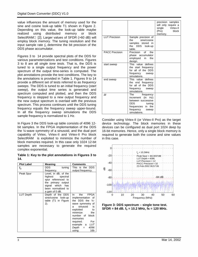
Figures 3 to 14 provide spectral plots of the DDS forvarious parameterizations and test conditions. Figures3 to 8 are all single tone tests. That is, the DDS istuned to a single output frequency and the powerspectrum of the output time-series is computed. Theplot annotations provide the test conditions. The key tothe annotations is provided in Table 1. Figures 9 to 14provide a different set of tests referred to as frequencysweeps. The DDS is tuned to an initial frequency (startsweep), the output time series is generated andspectrum computed and plotted, and then the DDSfrequency is stepped to a new output frequency andthe new output spectrum is overlaid with the previousspectrum. This process continues until the DDS tuningfrequency equals the frequency sweep upper-bound.In all the frequency sweep simulations the DDSsample frequency is normalized to 1 Hz.
In Figure 3 the DDS look-up table consists of 4096 12-bit samples. In the FPGA implementation of the DDSthe ¼-wave symmetry of a sinusoid, and the dual portcapability of Virtex, Virtex-II and Virtex-II Pro blockSelectRAM is exploited to minimize the number ofblock memories required. In this case only 1024 12-bitsamples are necessary to generate the requiredcomplex exponential.
Table 1: Key to the plot annotations in Figures 3 to14.
Plot Label Meaning Commentsf0 DDS tuning
frequency.This is the DDSoutput frequency.
Peak Spur Level, in dB, of thehighest spectralspur referenced tothe primary outputsignal which hasbeen normalized toa gain of 0 dB.
LUT Depth Depth of the DDSsine/cosine look-uptable (T1 in Figure2).
In the FPGAimplementation ofthe DDS the ¼-wave symmetry ofa sinusoid isexploited tominimize thenumber of blockmemoriesrequired. Forexample a LUTDepth = 4096using 16b
precision sampleswill only require asingle Virtex-II(Pro) blockmemory.
LUT Precision Sample precision ofthe sine/cosinesamples stored inthe DDS look-uptable.
PACC Precision Precision of thephase accumulatoremployed in thedesign.
start sweep This value definesthe start frequencyfor all of the DDSfrequency sweepsimulations.
end sweep This value definesthe end frequencyfor all of the DDSfrequency sweepsimulations.
∆f The frequencyincrement (in Hz)between successiveDDS tuningfrequencies in thefrequency sweepsimulations.
Consider using Virtex-II (or Virtex-II Pro) as the targetdevice technology. The block memories in thesedevices can be configured as dual port 1024 deep by16-bit memories. Hence, only a single block memory isrequired to generate both the cosine and sine valuesin this case.
0 10 20 30 40 50 60-120
-100
-80
-60
-40
-20
0
-84 dB
Frequency (MHz)
dB
f0 = 10.2MHz Peak Spur = -84.3037dBLUT Depth = 4096 LUT Precision = 12 PACC Precision = 32 22-Feb-2002 06:57:06
Figure 3: DDS spectrum – single tone test.SFDR = 84 dB. f0 = 10.2 MHz, fs = 120 MHz.

Digital Down Converter (DDC) V1.0
4 Mar 14, 2002
0 10 20 30 40 50 60
-120
-100
-80
-60
-40
-20
0
-96 dB
Frequency (MHz)
dB
f0 = 10.2MHz Peak Spur = -98.2487dBLUT Depth = 16384 LUT Precision = 16 PACC Precision = 32 22-Feb-2002 09:42:34
Figure 4: DDS spectrum – single tone test.SFDR = 96 dB. f0 = 10.2 MHz, fs = 120 MHz.
0 10 20 30 40 50 60
-120
-100
-80
-60
-40
-20
0
-96 dB
Frequency (MHz)
dB
f0 = 40.2MHz Peak Spur = -97.6334dBLUT Depth = 16384 LUT Precision = 16 PACC Precision = 32 22-Feb-2002 09:45:13
Figure 5: DDS spectrum – single tone test.SFDR = 96 dB. f0 = 40.2 MHz, fs = 120 MHz.
0 10 20 30 40 50 60-140
-120
-100
-80
-60
-40
-20
0
-108 dB
Frequency (MHz)
dB
f0 = 5.4MHz Peak Spur = -111.6378dBLUT Depth = 65536 LUT Precision = 18 PACC Precision = 32 22-Feb-2002 20:07:53
Figure 6: DDS spectrum – single tone test.SFDR = 108 dB. f0 = 5.4 MHz, fs = 120 MHz.
0 10 20 30 40 50 60-140
-120
-100
-80
-60
-40
-20
0
-108 dB
Frequency (MHz)
dB
f0 = 30MHz Peak Spur = -109.6127dBLUT Depth = 65536 LUT Precision = 18 PACC Precision = 32 22-Feb-2002 20:12:23
Figure 7: DDS spectrum – single tone test.SFDR = 108 dB SFDR. f0 = 30 MHz, fs = 120 MHz.
0 10 20 30 40 50 60-140
-120
-100
-80
-60
-40
-20
0
-108 dB
Frequency (MHz)
dBf0 = 55MHz Peak Spur = -109.1128dBLUT Depth = 65536 LUT Precision = 18 PACC Precision = 32 22-Feb-2002 20:15:38
Figure 8: DDS spectrum – single tone test.SFDR = 108 dB SFDR. f0 = 55 MHz, fs = 120 MHz.
0 0.2 0.4 0.6 0.8 1
-120
-100
-80
-60
-40
-20
0
-108 dB
start sweep = 0.313 end sweep = 0.3415 num sweeps = 10 ∆ f = 0.00285 LUT Depth = 65536 LUT Precision = 18 PACC Precision = 32 23-Feb-2002 23:34:15
Frequency
dB
Figure 9: DDS frequency sweep simulation.frequencies. The highest spur is 108 dB below theoutput signal.

Digital Down Converter (DDC) V1.0
5 Mar 14, 2002
0 0.2 0.4 0.6 0.8 1
-120
-100
-80
-60
-40
-20
0
-84 dB
start sweep = 0.113 end sweep = 0.1415 num sweeps = 10 ∆ f = 0.00285 LUT Depth = 4096 LUT Precision = 14 PACC Precision = 32 23-Feb-2002 23:16:59
Frequency
dB
Figure 10: Dithered DDS simulation. The highestspur is 84 dB below the output signal.
0 0.2 0.4 0.6 0.8 1
-120
-100
-80
-60
-40
-20
0
-72 dB
start sweep = 0.113 end sweep = 0.1415 num sweeps = 10 ∆ f = 0.00285 LUT Depth = 1024 LUT Precision = 12 PACC Precision = 32 23-Feb-2002 23:14:26
Frequency
dB
Figure 11: DDS frequency sweep simulation. Thehighest spur is 72 dB below the output signal.
0 0.2 0.4 0.6 0.8 1
-120
-100
-80
-60
-40
-20
0
-72 dB
start sweep = 0.05 end sweep = 0.07 num sweeps = 50 ∆ f = 0.0004 LUT Depth = 1024 LUT Precision = 12 PACC Precision = 32 23-Feb-2002 23:01:20
Frequency
dB
Figure 12: DDS frequency sweep simulation. Thehighest spur i s 72 dB below the output signal.
0 0.2 0.4 0.6 0.8 1
-120
-100
-80
-60
-40
-20
0
90 dB
start sweep = 0.05 end sweep = 0.25 num sweeps = 30 ∆ f = 0.0066667LUT Depth = 8192 LUT Precision = 15 PACC Precision = 32 23-Feb-2002 23:46:29
Frequency
dB
Figure 13: DDS frequency sweep simulation. Thehighest spur is 90 dB below the output signal.
0 0.2 0.4 0.6 0.8 1
-120
-100
-80
-60
-40
-20
0
-84 dB
start sweep = 0.05 end sweep = 0.07 num sweeps = 50 ∆ f = 0.0004 LUT Depth = 4096 LUT Precision = 14 PACC Precision = 32 23-Feb-2002 22:52:02
Frequency
dB
Figure 14: DDS frequency sweep simulation. Thehighest spur is 84 dB below the output signal.
DDS Tuning
The DDS can be configured to have a constant outputfrequency, or it can be programmed using the Coremicroprocessor style interface. The output frequency,fout, of the DDS waveform is a function of the systemsample rate fs, the number of bits ( )nBθ used in the
phase accumulator and the phase increment value
∆θ. That is ( )out s ( ), , .nf f Bθ θ= ∆F The output
frequency in Hertz is defined as
sout ( )
Hz2
B n
ffθ
θ∆= (1)

Digital Down Converter (DDC) V1.0
6 Mar 14, 2002
The DDS may be tuned to a single and fixed frequencywhen the Core is customized, or the tuning frequencymay be modified in real-time if the Programmableoption is selected on the DDS customization panel.For example, if the DDS parameters are
s
10
( )
120 MHz= 32
1000n
fBθ
θ
=
∆ =
(2)
the output frequency will be
sout
6
32
( )Hz
2120 10 1000=
227.939677 MHz
nBff
θ
θ∆=
× ×
=
(3)
The phase increment value ∆θ required to generatean output frequency fout Hz is
out
s
( )2 nBf
f
θθ∆ = (4)
The phase accumulator precision is reported on theDDC GUI panel shown in Figure 40. The phaseincrement value can be computed using thisinformation together with the Core clock frequency andEq. (4).
DDS Frequency Resolution
The DDS tuning frequency resolution ∆f is a function ofthe phase accumulator width (refer to Figure 2) andthe system sample rate fs. To decouple the user fromhaving to define the desired frequency resolution interms of a bit field width, the DDC customization GUIdirectly accepts the frequency resolution specificationin Hertz.
The frequency resolution can be determined using thefollowing equation
( )
s
2 nBffθ
∆ = (5)
If the frequency resolution is specified as 0.03 Hz andthe sample rate is 100 MHz, for example, then thephase accumulator width will be
( )( ) 2log
32nB f fθ = ∆ ×
=s
bits
(6)
CIC Decimator
The CIC filter is an optional component (selected usingthe customization GUI) that can be inserted into theDDC signal processing chain, or it can be entirelyexcluded.Cascaded integrator-comb (CIC), or Hogenauer filters[1], are multirate filters used for realizing large samplerate changes in digital systems. CIC filters aremultiplierless structures, consisting of only adders,subtractors and registers. They are typically employedin applications where there is a large excess samplerate. That is, the system sample rate is much largerthan the bandwidth occupied by the signal.
Figure 15 shows the basic structure for a CICdecimation filter. The integrator section consists of Nideal integrator stages operating at the high samplingrate f s . Each stage is implemented as a one-polefilter with a unity feedback coefficient. The transferfunctions for a single integrator is
H zzI ( ) =
− −
11 1 (7)
The comb section operates at the low sampling ratef Rs / where R is the integer rate change factor. This
section consists of N comb stages with a differentialdelay of M samples per stage. The differential delayis a filter design parameter used to control the filter’sfrequency response. M is restricted to be either 1 or2. The transfer function for a single comb stage,referenced to the high input sample rate is
H z zCRM( ) = − −1
There is a rate change switch (indicated in the Figure15 as the decimate function) between the two filtersections. The decimator sub-samples the output of thelast integrator stage, reducing the sample rate from f s
to f Rs / .
The system transfer function for the composite CICfilter, referenced to the high sampling rate, is

Digital Down Converter (DDC) V1.0
7 Mar 14, 2002
1
1
0
(1 )( ) ( )(1 )
RM NN NI C N
NRMk
k
zH z H z Hz
z
−
−
−−
=
−= =−
= ∑
(8)
From the last form of the CIC transfer function weobserve that the CIC filter is equivalent to a cascade ofN uniform FIR (finite impulse response) filter stageswith unit coefficients, that is, the filter is equivalent to acascade of N boxcar filters.
The CIC filter supports decimation factors from 4 to16383. The sample rate adjustment may be fixedwhen the Core customization is performed, or it can beprogrammable. When the programmable mode isselected the decimation rate maybe adjusted in real-time. The number of integrator/differentiator sections isselectable and ranges from 2 to 8.
Decimateby R
z-M
+-
z-M
+-
z-M
+-
y(n)x(n)P0 P1 P3
2 to 8 stagesSample rate = fs
2 to 8 stagesSample rate = fs/R
Input SampleRate fs
R = 4 to 16383 Output SampleRate fs/R
Figure 15: CIC decimation filter.
CIC filters have a lowpass frequency characteristic.The frequency response is obtained by evaluating Eq.(8) at
z ej f
R=2π
(9)
where f is the frequency relative to the low samplingrate f Rs / . As part of the filter design processR, M and N are chosen to provide acceptablepassband characteristics over the frequency rangefrom zero to a pre-determined cutoff frequency f cexpressed relative to the low sampling rate.
Evaluating Eq. (8) in the z-plane at the sample pointsdefined by Eq. (9) gives the magnitude frequencyresponse as
sin| ( ) |sin
N
MfH f fR
ππ
=
(10)
Eq. (10) indicates that there are nulls (transferfunctions zeros) at integer multiples of f M= 1/ .Thus, the differential delay parameter, M can be usedas a design parameter to control the placement of thefilter’s zeros. Figure 17 shows the frequency response
of a 4-stage (N = 4) CIC filter with unity differentialdelay (M = 1) and a sample rate change R = 7. Whenemployed as a decimator the frequency bands in theinterval
kM
f k Rc± = 1 2 2, , , /… (11)
will alias back into the filter passband. Care must betaken to ensure that the integrated sidelobe levels donot impact the intended application.

Digital Down Converter (DDC) V1.0
8 Mar 14, 2002
0 0.5 1 1.5 2 2.5 3 3.5-120
-100
-80
-60
-40
-20
0
Frequency
DB
2fc 2fc 2fcfc
Aliasing/ImagingBands
Pass-band
Figure 16: CIC filter frequency response for N = 4,M = 1, R = 7 and f c = 1 8/ .
Figure 17 shows the frequency response for a filterwith virtually the same parameters as that of Figure16, but in this case the differential delay is M = 2. Thetransmission zeros are now located at integermultiples of 1/M = ½, as is clearly observed in the plot.
0 0.5 1 1.5 2 2.5 3 3.5-120
-100
-80
-60
-40
-20
0
Frequency
DB
2fc 2fc 2fc 2fc 2fc 2fc fc
Aliasing/ImagingBands fc
Passband
Figure 17: CIC filter frequency response for N = 4,M = 2, R = 7 and f c = 1 8/ .
Figures 18 to 26 show the frequency response plotsfor various combinations of the design parameters N,
R and M. Figures 20 to 24 provide insight into the filterbehavior as the number of integrator and differentiator(N) stages are varied. In all these cases the differential
delay is held constant at M = 1 and the sample ratechange is fixed at R = 48. For any CIC filter there are
always RM zeros in the transfer function. The zerosare equally spaced around the unit circle in the z-plane
at integer multiples of 1/ RM - there is of course no
zero at z = 0. Increasing N has the effect ofincreasing the order of the zeros. This in turn
increases the attenuation at frequencies in the localityof the zero. This effect is clearly illustrated in Figures20 to 24 where we see increasing attenuation of the
filter sidelobes as N is increased. Also note that as theorder of the zeros increase, the passband droop also
increases thus narrowing the filter bandwidth. Theincreased droop may not be acceptable in some
applications. The droop is frequently corrected usingan additional (non CIC based) stage of filtering after
the CIC decimator.
0 0.1 0.2 0.3 0.4 0.5-150
-100
-50
0
Frequency
DB
R = 8M = 1N = 4
0 0.005 0.01 0.015-2
0
2
Frequency
DB
R = 8M = 1N = 4
Figure 18: CIC filter frequency response for N = 4,M = 1, R = 8.
0 0.1 0.2 0.3 0.4 0.5-150
-100
-50
0
Frequency
DB
R = 8M = 2N = 4
0 2 4 6 8
x 10-3
-2
-1
0
1
2
Frequency
DB
R = 8M = 2N = 4
Figure 19: CIC filter frequency response for N = 4,M = 2, R = 8.

Digital Down Converter (DDC) V1.0
9 Mar 14, 2002
0 0.1 0.2 0.3 0.4 0.5-150
-100
-50
0
Frequency
DB
R = 48M = 1 N = 1
0 0.5 1 1.5 2 2.5 3
x 10-3
-2
0
2
Frequency
DB
R = 48M = 1 N = 1
Figure 20: CIC filter frequency response for N = 1,M = 1, R = 48.
0 0.1 0.2 0.3 0.4 0.5-150
-100
-50
0
Frequency
DB
R = 48M = 1 N = 2
0 0.5 1 1.5 2 2.5 3
x 10-3
-2
0
2
Frequency
DB
R = 48M = 1 N = 2
Figure 21: CIC filter frequency response for N = 2,M = 1, R = 48.
0 0.1 0.2 0.3 0.4 0.5-150
-100
-50
0
Frequency
DB
R = 48M = 1 N = 3
0 0.5 1 1.5 2 2.5 3
x 10-3
-2
0
2
Frequency
DB
R = 48M = 1 N = 3
Figure 22: CIC filter frequency response for N = 3,M = 1, R = 48.
0 0.1 0.2 0.3 0.4 0.5-150
-100
-50
0
Frequency
DB
R = 48M = 1 N = 4
0 0.5 1 1.5 2 2.5 3
x 10-3
-2
-1
0
1
2
Frequency
DB
R = 48M = 1 N = 4
Figure 23: CIC filter frequency response for N = 4,M = 1, R = 48.

Digital Down Converter (DDC) V1.0
10 Mar 14, 2002
0 0.1 0.2 0.3 0.4 0.5-150
-100
-50
0
Frequency
DB
R = 48M = 1 N = 8
0 0.5 1 1.5 2 2.5 3
x 10-3
-2
0
2
Frequency
DB
R = 48M = 1 N = 8
Figure 24: CIC filter frequency response for N = 8,M = 1, R = 48.
0 0.1 0.2 0.3 0.4 0.5-150
-100
-50
0
Frequency
DB
R = 8M = 1N = 8
0 0.005 0.01 0.015-2
-1
0
1
2
Frequency
DB
R = 8M = 1N = 8
Figure 25: CIC filter frequency response for N = 8,M = 1, R = 8.
0 0.1 0.2 0.3 0.4 0.5-150
-100
-50
0
Frequency
DB
R = 8M = 2N = 8
0 2 4 6 8
x 10-3
-2
-1
0
1
2
Frequency
DB
R = 8M = 2N = 8
Figure 26: CIC filter frequency response for N = 8,M = 2, R = 8.
A compensation filter can be used to flatten thepassband frequency response. For a CIC decimatorthe compensation filter operates at the decimatedsample rate. The compensation filter provides( / sin( ))x x N shaping. An example of a 3rd order (N =3) R = 64 compensated CIC system is shown in Figure27. The plot shows the uncompensated CIC frequencyresponse, the compensation filter frequency responseand the compensated CIC. In this case, since thenumber of CIC stages is 3, the compensation filter hasa cubic response of the form ( / sin( )) .x x 3
0 0.01 0.02 0.03 0.04 0.05 0.06-60
-50
-40
-30
-20
-10
0
10
Frequency
DB Composite Filter
Compensation Filter
C IC Filter
Figure 27: CIC compensation filter. N = 3, R = 64.The compensation filter coefficients employed were

Digital Down Converter (DDC) V1.0
11 Mar 14, 2002
[-1, 4, 16, 32, –64, 136, –352, 1312, –352, 136, –64,32, –16, 4, -1]
Figure 28 provides an exploded view of thecompensated filter passband.
0 1 2 3 4 5 6 7
x 10-3
-2
-1.5
-1
-0.5
0
0.5
Frequency
DB
Composite Filter
CIC Filter
Compensation Filter
Figure 28: CIC compensation filter. N = 3, R = 64.Passband response.
The CIC compensation filter can be implementedusing the DDC CFIR filter.
Register Growth
The CIC datapath experiences internal register growththat is a function of all the design parameters: N, M, Rand the input sample precision B3. The full precisionoutput width BMAX at the filter output is defined in Eq.(12)
B N RM BMAX = + −log2 1 (12)
where . denotes the ceiling operator. The CIC filteruses BMAX bits internally for each of the integrator anddifferentiator stages, and so produces a full-precisionresult at the filter output. Using the customization GUI,the user may elect to carry a lower precision sampleforward to the next processing stage. Convergentrounding is used to generate the reduced precisionsample. If a bit precision greater than BMAX is specifiedfor the CIC output width, this value will beautomatically limited to BMAX bits.
CIC Gain Stage
A course gain adjustment may be applied at the outputof the CIC filter to compensate for the bandwidthreduction performed by the CIC decimator. The signalgain can be boosted by 42 dB (7-bit left shift) prior torounding (convergent) to the final output width CICGain Output Width (node B5 in Figure 1). The gain is2COURSE where COURSE is a value between 0 and 7inclusive. If the signal power across the inputbandwidth is relatively flat, as is the case in mostfrequency division multiplexed (FDM) systems, thenone would want to boost the signal power out of theCIC filter by a factor of ,R where R is the decimationrate of the CIC filter. Table 3 supplies the registeraddress map for setting the CIC gain factor whileTable 4 defines the permissible gain values.
Compensation Filter (CFIR) andProgrammable FIR (PFIR)
The signal stream from the CIC can be filtered by twoadditional stages of filtering. The compensation finiteimpulse response (CFIR) filter and the programmablefinite impulse response (PFIR) filter. These areoptional stages of processing that may be inserted orexcluded from the datapath.
Both these filters utilize the distributed arithmetic (DA)FIR filter [3] supplied with the Core Generator [4]. Fora full description of the DA FIR filter please refer to [3].
DA filters employ a table look-up procedure [3], whichis well suited to the architecture of Xilinx FPGAs. Theuser should be aware that even when an FPGA familylike Virtex-II or Virtex-II Pro is selected, that includes adedicated array of multipliers, the look-up tableprocess of the DA FIR algorithm will still be employedfor the CFIR and PFIR implementation.
The CFIR and PFIR can be single rate or polyphasemultirate filter structures. The sample rate change foreach filter is user selectable from decimate by 1through 8. Decimate by 1 is of course a single-rate FIRfilter. The filter length for each filter ranges from 0 to1024 taps. The coefficient precision may also becustomized and ranges from 1 to 32 bits. Each filtermay also be selected as a polyphase halfband filter.

Digital Down Converter (DDC) V1.0
12 Mar 14, 2002
Filter Length, FPGA Area and SampleRate
Reducing the filter length minimizes the FPGA logicresources required to implement the filter. However,the filter length does not impact the filter sample rateas is the case with a time-division multiplexed multiply-accumulate (MAC)–based approach to the problem.Using a time-shared MAC approach, like thatemployed in an instruction set architecture (ISA)solution, all of the operations are folded onto a single(or small number of) MAC unit(s). The sample rate istherefore inversely proportional to the filter length: asthe filter length increases, the maximum sample ratethat can be supported is reduced. However, with DAarchitectures the sample rate is effectively decoupledfrom the filter length [3]. This means that increasingthe filter length does not impact the systemthroughput. Irrespective of whether the CFIR is a 21-tap filter or an 81-tap filter, the throughput will remainconstant. This is achieved by incorporating moreparallelism into the design. Increasing the filter willresult in an increase in FPGA resource utilization.
CFIR
Typically, the CFIR filter will be selected as a multiratestructure (like that shown in Figure 30) and introduce asample rate reduction ranging from 2 to 4 (althoughup to 8 is supported). In many cases the CFIR willhave a wide transition band in order to minimize thefilter length. Figure 29 shows a typical magnitudefrequency response plot for the CFIR when thedecimation rate is D1 = 2. The sample rate at the inputof the CFIR (different to the DDC input sample rate) isfCFIR. In a modern receiver a wideband digitizationprocess (wide band A/D) will be used and thechannelization processing will be implementeddigitally. Typically this channel of interest will benarrrow in comparison to the wideband inputspectrum. This is shown in Figure 29 where the signalof interest extends out to fc, a much smaller frequencythan fCFIR. In this case the frequency band betweenfCFIR/2- fc and fc/2 (the hatched region in the Figure 29)will be aliased back to baseband. The CFIR frequencyresponse need only supply acceptable out-of-bandrejection over this interval. This means that thetransition bandwidth fT can be wide, so minimizing thelength of the filter, which in turn will reduce the FPGAresources required to implement the filter.
0 dB
fCFIR/2fCFIR/4
Signal of Interest
fcfCFIR/2-fc
StopbandfT
Figure 29: CFIR frequency response: Typicalcharacteristic.
h0(n)
h1(n)
hM-3(n)
x(n)
hM-2(n)
hM-1(n)
y(n)
Figure 30: Polyphase decimator used for both theCFIR and the PFIR.
Symbol and Port Definitions
The DDC symbol and ports are shown in Figure 31.
DIN
WE
CLK
RFD
DOUT_I
RDY
ND
SELADDRLD_DIN
DOUT_Q
††
††
†Optional Port
Figure 31: DDC symbol and ports.
The Core port definitions are provided in Table 2.
Digital Down Converter (DDC) V1.0
13 Mar 14, 2002
Table 2: DDC Core ports and definitions.
Signal Name Direction DescriptionCLK Input CLOCK Master Clock
(active rising edge)DIN Input DATA INPUT DDC input
data port.
ND Input NEW DATA (active high)– When this signal isasserted the datasample presented on theDIN port is loaded intothe DDC.
SEL Input SEL (active high) is amaster chip select and itmust be high whileupdating internal controlregisters.
ADDR Input The ADDR port is anaddress bus for theinternal register set.
LD_DIN Input LOAD DATA INPUT.This input databus isused to update thevarious internalregisters.
WE Input WRITE ENABLESTROBE (active high)WE is associated withthe LD_DIN port. It is thewrite enable signal fordata on LD_DIN. WhenWE is high, the data onthe LD_DIN port will beaccepted by the DDCsynchronously with therising edge of CLK. SELmust be high to performa write operation tointernal registers.
DOUT_I Output OUTPUT PORT I In-phase component of theDDC output.
DOUT_Q Output OUTPUT PORT QQuadrature componentof the DDC output.
RDY Output DDC OUTPUT SAMPLEREADY (active high)Indicates that a newfilter output sample isavailable on the DOUTport.
RFD Output READY FOR DATA –(active high) Indicateswhen the DDC canaccept a new inputsample.
Control Interface
The DDC filter employs a data-flow style interface forsupplying input samples to the Core and for readingthe output ports. ND (New Data), RFD (Read ForData) and RDY (Ready) are used to co-ordinate I/Ooperations.
The Core output status signal RFD signals to thesystem that the DDC is ready for data. RFD is activehigh. Asserting ND high indicates to the Core theavailability of a new input sample on the DIN port. NDis very similar in functionality to the clock enable signalfound on many VLSI (very large scale integratedcircuit) devices. The RDY output signal indicates that anew DDC output sample is available on the DOUT_Iand DOUT-Q ports.
The interface signals would typically be used in thefollowing manner. The user system would first wait forRFD=1. This signals that a new input sample can bewritten to the DDC. The new input sample would beplaced on the DIN port and ND would be placed in theactive state (ND=1) for a single clock cycle. AssertingND indicates to the Core that it should sample the DINport. The DDC will sample DIN on the rising edge ofthe clock (CLK) qualified with ND=1. A DDC readoperation can occur when the Core asserts RDY=1.RDY could be used as a clock enable signal for adown-stream processing block that is consuming theDDC output samples.
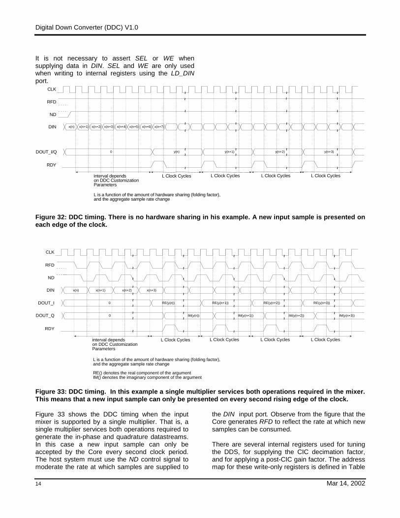
Figure 32 shows the timing when a continuous streamof input samples is to be processed. In this case ainput sample is available in each clock period. In theexample a new input sample is applied on every clockedge, so ND must be continuously held high. A certainnumber of clock cycles after the first input sample hasbeen written to the filter, RDY will be asserted by theDDC to indicate that the first output sample isavailable. This time interval is a function of the down-sampling factor R employed in the CIC filter, thenumber of taps in the CFIR and PFIR and the samplerate change used in these filters as well as a fixedlatency that is related to internal pipeline registers inthe Core. The number of pipeline stages depends onthe Core customization parameters. After the very firstoutput sample has been produced, subsequentoutputs will be available every L clock cycles. It isstrongly recommended that designers employ the RDYsignal as a gating signal for any processes thatconsume the filter output samples.
Digital Down Converter (DDC) V1.0
14 Mar 14, 2002
It is not necessary to assert SEL or WE whensupplying data in DIN. SEL and WE are only usedwhen writing to internal registers using the LD_DINport.
RDY
ND
CLK
DOUT_I/Q
RFD
DIN x(n) x(n+1) x(n+2) x(n+3) x(n+4) x(n+5) x(n+6) x(n+7)
y(n) y(n+1) y(n+2)
interval dependson DDC CustomizationParameters
y(n+3)0
L Clock Cycles L Clock Cycles L Clock Cycles L Clock Cycles
L is a function of the amount of hardware sharing (folding factor),and the aggregate sample rate change
Figure 32: DDC timing. There is no hardware sharing in his example. A new input sample is presented oneach edge of the clock.
RDY
ND
CLK
DOUT_Q
RFD
DIN x(n) x(n+1) x(n+2) x(n+3)
IM(y(n)) IM(y(n+1)) IM(y(n+2))
interval dependson DDC CustomizationParameters
IM(y(n+3))0
L Clock Cycles L Clock Cycles L Clock Cycles L Clock Cycles
DOUT_I RE(y(n)) RE(y(n+1)) RE(y(n+2)) RE(y(n+3))0
L is a function of the amount of hardware sharing (folding factor),and the aggregate sample rate change
RE() denotes the real component of the argumentIM() denotes the imaginary component of the argument
Figure 33: DDC timing. In this example a single multiplier services both operations required in the mixer.This means that a new input sample can only be presented on every second rising edge of the clock.
Figure 33 shows the DDC timing when the inputmixer is supported by a single multiplier. That is, asingle multiplier services both operations required togenerate the in-phase and quadrature datastreams.In this case a new input sample can only beaccepted by the Core every second clock period.The host system must use the ND control signal tomoderate the rate at which samples are supplied to
the DIN input port. Observe from the figure that theCore generates RFD to reflect the rate at which newsamples can be consumed.
There are several internal registers used for tuningthe DDS, for supplying the CIC decimation factor,and for applying a post-CIC gain factor. The addressmap for these write-only registers is defined in Table

Digital Down Converter (DDC) V1.0
15 Mar 14, 2002
3. All of these registers are accessed using theLD_DIN bus in conjunction with SEL and WE controlsignals. The bit width of LD_DIN is a function of thecustomization parameters. Typically, the precision ofthe DDS phase accumulator register
(DDS_PHASE_INC in Table 3) will govern the widthof the LD_DIN port. All write-only registers,regardless of precision, are aligned by their least-significant bit.
Table 3: Internal register address map. All registers are write-only.
Address Data Width Register Name Comment6 Width is a
function of thefrequencyresolution andthe sample rate.
DDS_PHASE_INC Write address for the DDS phase incrementregister. The DDC tuning frequency is definedby writing a phase increment value to thisaddress.
8 Based onmaximum ratechange
CIC_RATE When the programmable rate change option isselected for the CIC filter, the decimation rateis supplied by updating this register.
9 3 COURSE_GAIN This 3-bit field defines the gain applied to theCIC output result. Refer to Table 4 for thecorrespondence between this value and thegain applied to the signal.
Table 4: CIC Coarse gain definitions.
Coarse Gain Value Gain (dB)0 01 62 123 184 245 306 367 42
DDC Control Register
Figure 34 shows the timing for a register writeoperation. The new register value is written to the
selected internal register when SEL=1 and WE=1. Thetransfer occurs synchronously with the clock.
WE
CLK
SEL
ADDR VALID
LD_DIN VALID
Figure 34: Register write operation.
User Interface
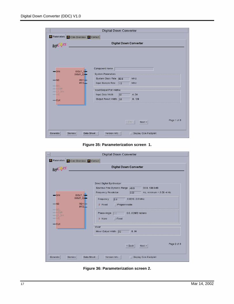
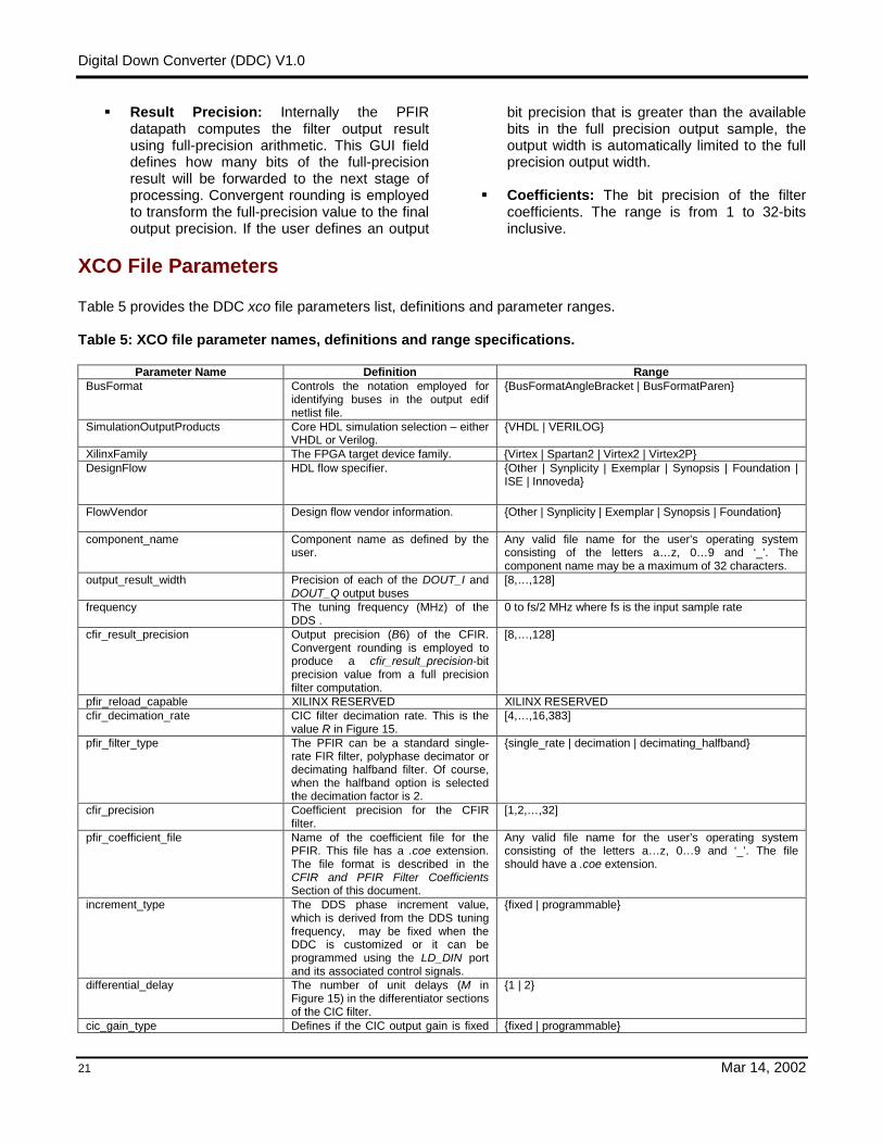
Figures 35 to 40 provide screenshots of the DDCcustomization wizard. The GUI parameter fields aredefined in the Parameters section of this document.
Parameters
• Component Name: The user defined DDCcomponent name.
• System Clock Rate: This is the master clockfrequency supplied via the CLK pin to the Core.
• Input Sample Rate: The input sample rate of thesignal presented on the DIN port. The relationshipbetween the system clock frequency fclk, signalsample rate fs and the decimation factors R, D1and D2 (refer to Figure 1) will determine if theCore can fold multiple operations onto the samefunctional unit. In other words, perform timedivision multiplexing of internal hardwarecomponents. For example, if fclk ≥ 2fs a singlemultiplier will be used in the mixer to generateboth the I and Q data streams.
• Input Data Width: The bit precision of the inputsamples provided on the port DIN. This valuecorresponds to B1 in Figure 1.
Digital Down Converter (DDC) V1.0
16 Mar 14, 2002
• Output Result Width: The bit precision of thefinal output samples produced on the output portsDOUT_I and DOUT_Q. This value corresponds toB8 in Figure 1.
• Direct Digital Synthesizer
! Spurious Free Dynamic Range (SFDR): Thisvalue (in dB) specifies the required value ofthe highest spur relative to a 0 dB referencedlocal oscillator frequency. For example, if theSFDR is specified as 70 dB, the spur levelgenerated by the DDS will be at least 70 dBbelow the DDS output signal. Refer to thesection of this document on Mixer and DirectDigital Synthesizer for more information. TheDDS sample precision B2 is computedaccording to B2 = SFDR/6 bits.
! Frequency Resolution: This value definesthe frequency resolution of the DDS
! Frequency: This value specifies the tuningfrequency of the DDS. When the Fixed modeis selected the DDS will be tuned to the valuedefined in the associated text box. When theProgrammable option is used the DDS tuningfrequency is supplied using themicroprocessor style interface that comprisesthe ports SEL, ADDR, LD_DIN and WE.
! Phase Angle: As shown in Figure 2, the DDSprovides an optional phase angle offset port.The phase offset value is defined (Fixedoption on the GUI) when the Core iscustomized. The phase angle range is 0 < θ< 6.283185307 (2π) radians.
! Mixer Output Width: This is the bit-precisionof the mixer output ports – parameter B3 inFigure 1.
• Cascaded Integrator/Comb Filter
The CIC filter is an optional stage ofdecimation that may be included after themixer.
Include CIC Filter: The Include CIC checkboxat the top of customization screen 3 is used toinclude or exclude the CIC filter. Whenchecked, the CIC will be included in thedatapath.
! Number of Stages: Referring to Figure 15,this is the number (between 2 and 8 inclusive)of integrator/differentiator stages included inthe CIC filter. For example, if the value 4 isspecified, the CIC filter will consist of 4 stagesof integration and a resampling switchfollowed by 4 differentiators.
! Differential Delay: The differential delay isthe number of delay stages (M in Figure 15)employed in each CIC differentiator.
! Decimation Rate: The decimation rate of theCIC filter, a value between 4 and 16383.
! CIC Output Width: The number of bits (B4)carried out from the CIC filter. Internally, theCIC filter generates a full-precision result andthen convergent rounding is used to produce afinal output bit-field of CIC Output Width bits.Internally, the full precision CIC output wordcarries B N RM BMAX = + −log2 1 bits,where N is the number ofintegrator/differentiator sections, M is thedifferential delay in the differentiator sections,R is the sample rate change and B is theprecision (B3) of the CIC input samples. If theCIC output bit precision is defined by the userto be greater than MAX ,B the Core willconstrain the output precision to precisely
MAXB bits.
! Gain Value: A course gain adjustment may beapplied at the output of the CIC filter tocompensate for the bandwidth reductionperformed by the CIC decimator. The signal gaincan be boosted by 42 dB (7-bit left shift) prior torounding (convergent) to the final output width CICGain Output Width. The gain is 2COURSE whereCOURSE is a value between 0 and 7 inclusive. Ifthe signal power across the input bandwidth isrelatively flat, as is the case in most frequencydivision multiplexed (FDM) systems, then onewould want to boost the signal power out of theCIC filter by a factor of ,R where R is thedecimation rate of the CIC filter.The gain can be fixed when the core is customizedor the programmable option may be selected.When the programmable option is used the gaincan be adjusted in real-time using themicroprocessor style interface. For theprogrammable option the gain value supplied viathe GUI is the initial gain value.
Digital Down Converter (DDC) V1.0
17 Mar 14, 2002
Figure 35: Parameterization screen 1.
Figure 36: Parameterization screen 2.

Digital Down Converter (DDC) V1.0
18 Mar 14, 2002
Figure 37: Parameterization screen 3.
Figure 38: Parameterization screen 4.

Digital Down Converter (DDC) V1.0
19 Mar 14, 2002
Figure 39: Parameterization screen 5.
Figure 40: Parameterization screen 6.

Digital Down Converter (DDC) V1.0
20 Mar 14, 2002
! CIC Gain Output Width: The bit precision ofthe final result from the CIC gain block, asdescribed in the previous paragraph. Thisvalue defines node B5 in Figure 1.
• Compensation Filter (CFIR)
The CFIR filter is an optional stage of filteringthat may be inserted in the signal processingchain. As well as a general purpose stage offiltering (and optional sample rate change) theCFIR can be used to compensate for anypassband droop that may have beenintroduced by the previous stage of processingwith the CIC filter.
Include CFIR: The Include CFIR checkbox atthe top of customization screen 4 is used toinclude or exclude the CFIR filter. Whenchecked, the CFIR will be included in thedatapath.
! Filter Type: The CFIR may be a standardsingle-rate FIR filter, a polyphase decimator,or a polyphase decimating halfband filter.When the polyphase decimator option isselected (Decimation option on the GUI) thedecimation rate may be a value between 2and 8 inclusive. The filter length isprogrammable and can be between 0 (noCFIR included) and 1024 taps.
! Decimation Rate: When the polyphasedecimator option is selected for the CFIR filter,this value specifies the sample rate change -a value between 2 and 8 inclusive.
! Response: In the majority of cases, thecoefficient set for the CFIR filter will besymmetric. This characteristic can beexploited to construct a smaller filter.However, since the filter is realized using adistributed arithmetic mechanization, asdiscussed in a previous section, exploitingfilter symmetry does impact throughputslightly. Using the radio buttons in theResponse GUI field, the user may explicitlydefine if coefficient symmetry is to be utilized(or not) when the filter circuit is constructed. Inthe majority of cases it will be desirable toenable coefficient symmetry (Symmetry radiobutton selected).
! Result Precision: Internally the CFIRdatapath computes the filter output resultusing full-precision arithmetic. This GUI fielddefines how many bits (B6) of the full-
precision result will be forwarded to the nextstage of processing. Convergent rounding isemployed to transform the full-precision valueto the final output precision. If the user definesan output bit precision that is greater than theavailable bits in the full precision outputsample, the output width is automaticallylimited to the full precision output width.
! Coefficients: The bit precision of the filtercoefficients. The range is from 1 to 32-bitsinclusive.
• Programmable Filter (PFIR)
The PFIR filter is an optional stage of filteringthat may be inserted in the signal processingchain.
Include PFIR: The Include PFIR checkbox atthe top of customization screen 5 is used toinclude or exclude the PFIR filter. Whenchecked, the PFIR will be included in thedatapath.
! Filter Type: The PFIR may be a standardsingle-rate FIR filter, a polyphase decimator,or a polyphase decimating halfband filter.When the polyphase decimator option isselected (Decimation option on the GUI) thedecimation rate may be a value between 2and 8 inclusive. The filter length isprogrammable and can be between 0 (noPFIR included) and 1024 taps.
! Decimation Rate: When the polyphasedecimator option is selected for the PFIR filter,this value specifies the sample rate change -a value between 2 and 8 inclusive.
! Response: In the majority of cases, thecoefficient set for the PFIR filter will besymmetric. This characteristic can beexploited to construct a smaller filter.However, since the filter is realized using adistributed arithmetic mechanization, asdiscussed in a previous section, exploitingfilter symmetry does impact throughputslightly. Using the radio buttons in theResponse GUI field, the user may explicitlydefine if coefficient symmetry is to be utilized(or not) when the filter circuit is constructed. Inthe majority of cases it will be desirable toenable coefficient symmetry (Symmetry radiobutton selected).
Digital Down Converter (DDC) V1.0
21 Mar 14, 2002
! Result Precision: Internally the PFIRdatapath computes the filter output resultusing full-precision arithmetic. This GUI fielddefines how many bits of the full-precisionresult will be forwarded to the next stage ofprocessing. Convergent rounding is employedto transform the full-precision value to the finaloutput precision. If the user defines an output
bit precision that is greater than the availablebits in the full precision output sample, theoutput width is automatically limited to the fullprecision output width.
! Coefficients: The bit precision of the filtercoefficients. The range is from 1 to 32-bitsinclusive.
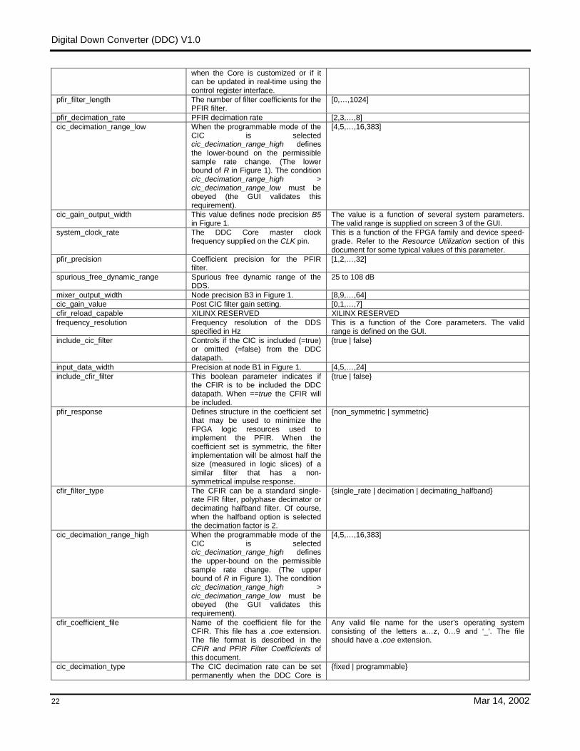
XCO File Parameters
Table 5 provides the DDC xco file parameters list, definitions and parameter ranges.
Table 5: XCO file parameter names, definitions and range specifications.
Parameter Name Definition RangeBusFormat Controls the notation employed for
identifying buses in the output edifnetlist file.
{BusFormatAngleBracket | BusFormatParen}
SimulationOutputProducts Core HDL simulation selection – eitherVHDL or Verilog.
{VHDL | VERILOG}
XilinxFamily The FPGA target device family. {Virtex | Spartan2 | Virtex2 | Virtex2P}DesignFlow HDL flow specifier. {Other | Synplicity | Exemplar | Synopsis | Foundation |
ISE | Innoveda}
FlowVendor Design flow vendor information. {Other | Synplicity | Exemplar | Synopsis | Foundation}
component_name Component name as defined by theuser.
Any valid file name for the user’s operating systemconsisting of the letters a…z, 0…9 and ‘_’. Thecomponent name may be a maximum of 32 characters.
output_result_width Precision of each of the DOUT_I andDOUT_Q output buses
[8,…,128]
frequency The tuning frequency (MHz) of theDDS .
0 to fs/2 MHz where fs is the input sample rate
cfir_result_precision Output precision (B6) of the CFIR.Convergent rounding is employed toproduce a cfir_result_precision-bitprecision value from a full precisionfilter computation.
[8,…,128]
pfir_reload_capable XILINX RESERVED XILINX RESERVEDcfir_decimation_rate CIC filter decimation rate. This is the
value R in Figure 15.[4,…,16,383]
pfir_filter_type The PFIR can be a standard single-rate FIR filter, polyphase decimator ordecimating halfband filter. Of course,when the halfband option is selectedthe decimation factor is 2.
{single_rate | decimation | decimating_halfband}
cfir_precision Coefficient precision for the CFIRfilter.
[1,2,…,32]
pfir_coefficient_file Name of the coefficient file for thePFIR. This file has a .coe extension.The file format is described in theCFIR and PFIR Filter CoefficientsSection of this document.
Any valid file name for the user’s operating systemconsisting of the letters a…z, 0…9 and ‘_’. The fileshould have a .coe extension.
increment_type The DDS phase increment value,which is derived from the DDS tuningfrequency, may be fixed when theDDC is customized or it can beprogrammed using the LD_DIN portand its associated control signals.
{fixed | programmable}
differential_delay The number of unit delays (M inFigure 15) in the differentiator sectionsof the CIC filter.
{1 | 2}
cic_gain_type Defines if the CIC output gain is fixed {fixed | programmable}
Digital Down Converter (DDC) V1.0
22 Mar 14, 2002
when the Core is customized or if itcan be updated in real-time using thecontrol register interface.
pfir_filter_length The number of filter coefficients for thePFIR filter.
[0,…,1024]
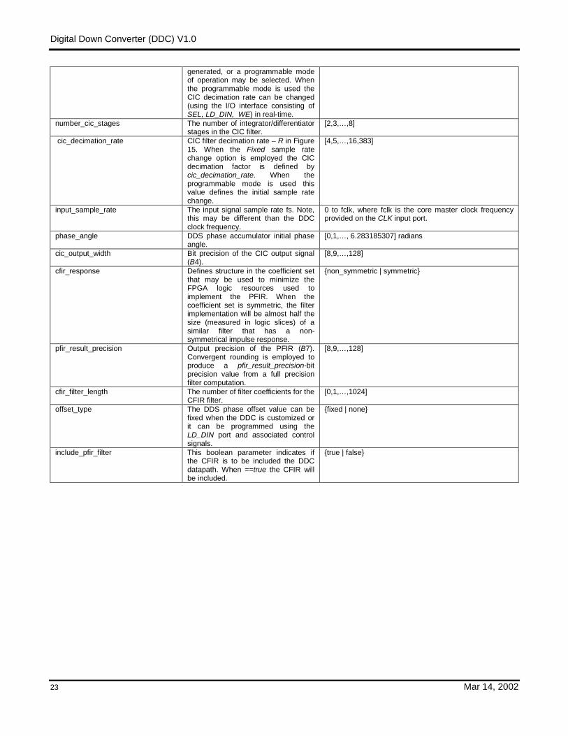
pfir_decimation_rate PFIR decimation rate [2,3,…,8]cic_decimation_range_low When the programmable mode of the
CIC is selectedcic_decimation_range_high definesthe lower-bound on the permissiblesample rate change. (The lowerbound of R in Figure 1). The conditioncic_decimation_range_high >cic_decimation_range_low must beobeyed (the GUI validates thisrequirement).
[4,5,…,16,383]
cic_gain_output_width This value defines node precision B5in Figure 1.
The value is a function of several system parameters.The valid range is supplied on screen 3 of the GUI.
system_clock_rate The DDC Core master clockfrequency supplied on the CLK pin.
This is a function of the FPGA family and device speed-grade. Refer to the Resource Utilization section of thisdocument for some typical values of this parameter.
pfir_precision Coefficient precision for the PFIRfilter.
[1,2,…,32]
spurious_free_dynamic_range Spurious free dynamic range of theDDS.
25 to 108 dB
mixer_output_width Node precision B3 in Figure 1. [8,9,…,64]cic_gain_value Post CIC filter gain setting. [0,1,…,7]cfir_reload_capable XILINX RESERVED XILINX RESERVEDfrequency_resolution Frequency resolution of the DDS
specified in HzThis is a function of the Core parameters. The validrange is defined on the GUI.
include_cic_filter Controls if the CIC is included (=true)or omitted (=false) from the DDCdatapath.
{true | false}
input_data_width Precision at node B1 in Figure 1. [4,5,…,24]include_cfir_filter This boolean parameter indicates if
the CFIR is to be included the DDCdatapath. When ==true the CFIR willbe included.
{true | false}
pfir_response Defines structure in the coefficient setthat may be used to minimize theFPGA logic resources used toimplement the PFIR. When thecoefficient set is symmetric, the filterimplementation will be almost half thesize (measured in logic slices) of asimilar filter that has a non-symmetrical impulse response.
{non_symmetric | symmetric}
cfir_filter_type The CFIR can be a standard single-rate FIR filter, polyphase decimator ordecimating halfband filter. Of course,when the halfband option is selectedthe decimation factor is 2.
{single_rate | decimation | decimating_halfband}
cic_decimation_range_high When the programmable mode of theCIC is selectedcic_decimation_range_high definesthe upper-bound on the permissiblesample rate change. (The upperbound of R in Figure 1). The conditioncic_decimation_range_high >cic_decimation_range_low must beobeyed (the GUI validates thisrequirement).
[4,5,…,16,383]
cfir_coefficient_file Name of the coefficient file for theCFIR. This file has a .coe extension.The file format is described in theCFIR and PFIR Filter Coefficients ofthis document.
Any valid file name for the user’s operating systemconsisting of the letters a…z, 0…9 and ‘_’. The fileshould have a .coe extension.
cic_decimation_type The CIC decimation rate can be setpermanently when the DDC Core is
{fixed | programmable}
Digital Down Converter (DDC) V1.0
23 Mar 14, 2002
generated, or a programmable modeof operation may be selected. Whenthe programmable mode is used theCIC decimation rate can be changed(using the I/O interface consisting ofSEL, LD_DIN, WE) in real-time.
number_cic_stages The number of integrator/differentiatorstages in the CIC filter.
[2,3,…,8]
cic_decimation_rate CIC filter decimation rate – R in Figure15. When the Fixed sample ratechange option is employed the CICdecimation factor is defined bycic_decimation_rate. When theprogrammable mode is used thisvalue defines the initial sample ratechange.
[4,5,…,16,383]
input_sample_rate The input signal sample rate fs. Note,this may be different than the DDCclock frequency.
0 to fclk, where fclk is the core master clock frequencyprovided on the CLK input port.
phase_angle DDS phase accumulator initial phaseangle.
[0,1,…, 6.283185307] radians
cic_output_width Bit precision of the CIC output signal(B4).
[8,9,…,128]
cfir_response Defines structure in the coefficient setthat may be used to minimize theFPGA logic resources used toimplement the PFIR. When thecoefficient set is symmetric, the filterimplementation will be almost half thesize (measured in logic slices) of asimilar filter that has a non-symmetrical impulse response.
{non_symmetric | symmetric}
pfir_result_precision Output precision of the PFIR (B7).Convergent rounding is employed toproduce a pfir_result_precision-bitprecision value from a full precisionfilter computation.
[8,9,…,128]
cfir_filter_length The number of filter coefficients for theCFIR filter.
[0,1,…,1024]
offset_type The DDS phase offset value can befixed when the DDC is customized orit can be programmed using theLD_DIN port and associated controlsignals.
{fixed | none}
include_pfir_filter This boolean parameter indicates ifthe CFIR is to be included the DDCdatapath. When ==true the CFIR willbe included.
{true | false}
Digital Down Converter (DDC) V1.0
24 Mar 14, 2002
SET BusFormat = BusFormatParenSET SimulationOutputProducts = VHDLSET XilinxFamily = Virtex2SET OutputOption = DesignFlowSET DesignFlow = VHDLSET FlowVendor = SynplicitySET FormalVerification = NoneSELECT Digital_Down_Converter Virtex2 Xilinx,_Inc. 1.0CSET output_result_width = 20CSET frequency = 2CSET cfir_result_precision = 20CSET pfir_reload_capable = FalseCSET cfir_decimation_rate = 2CSET pfir_filter_type = DecimationCSET cfir_precision = 16CSET pfir_coefficient_file = C:\pfirgsm.coeCSET increment_type = ProgrammableCSET differential_delay = 1CSET cic_gain_type = FixedCSET pfir_filter_length = 63CSET pfir_decimation_rate = 2CSET cic_decimation_range_low = 4CSET cic_gain_output_width = 20CSET system_clock_rate = 104CSET pfir_precision = 16CSET spurious_free_dynamic_range = 84CSET component_name = ddc_gsmCSET mixer_output_width = 20CSET cic_gain_value = 16CSET cfir_reload_capable = FalseCSET frequency_resolution = 0.02CSET include_cic_filter = TrueCSET input_data_width = 12CSET include_cfir_filter = TrueCSET pfir_response = SymmetricCSET cfir_filter_type = DecimationCSET cic_decimation_range_high = 16383CSET cfir_coefficient_file = C: \cfirgsm.coeCSET cic_decimation_type = FixedCSET number_cic_stages = 4CSET cic_decimation_rate = 48CSET input_sample_rate = 52CSET phase_angle = 0.0CSET cic_output_width = 24CSET cfir_response = SymmetricCSET pfir_result_precision = 24CSET cfir_filter_length = 21CSET offset_type = NoneCSET include_pfir_filter = TrueGENERATE
Figure 41: Example DDC .xco file.
CFIR and PFIR Filter Coefficients
The filter coefficients are supplied to the filter compilerusing a coefficient file with a .coe extension. This is anASCII text file with a single line header that defines theradix of the number representation used for thecoefficient data, followed by the coefficient valuesthemselves. This is shown in Figure 42 for an N-tapfilter.
The filter coefficients must be supplied as integers ineither base-10, base-16 or base-2 representation. This
corresponds to coefficient_radix=10,coefficient_radix=16 and coefficient_radix=2respectively.
radix=coefficient_radix;coefdata=a(0),a(1),a(2),….a(N-1);
Figure 42: Filter coefficient file format.
The coefficient values may also be placed on a singleline as shown in Figure 43.
radix=coefficient_radix;coefdata=a(0),a(1),a(2),….,a(N-1);
Figure 43: Filter coefficient file format – coefficientdata on a single line.
The coefficient file format for each of the filter classessupported by the core are discussed below.
Single-Rate and Polyphase Filters
The coefficient file for the single-rate and polyphasedecimator structures FIR filter is straightforward andconsists of a one-line header followed by the filtercoefficient data. For example, the filter coefficient filefor an 8-tap filter using a base-10 representation forthe coefficient values is shown in Figure 44.
radix=10;coefdata=20,-256,200,255,255,200,-256,20;
Figure 44: Filter coefficient file – 8-tap filter, base-10 coefficient values.
Even when the coefficient values are symmetrical, thecoefficient file should contain the complete set ofcoefficient values. The filter coefficient file for the non-symmetric impulse response shown in Figure 45 ispresented in Figure 46.

Digital Down Converter (DDC) V1.0
25 Mar 14, 2002
255
200
-180
80
220
180100
-48
40
Figure 45: Non-symmetric impulse response.
radix=10;coefdata=255,200,-180,80,220,180,100,-48,40;
Figure 46: Coefficient file for the non-symmetricimpulse response in Figure 45.
Decimating Half-Band Filter
Every second filter coefficient for a half-band filter withan odd number of terms will be zero. When specifyingthe filter coefficient data for this filter class, the zerovalue entries need to be included in the coefficient file.For example, the filter coefficient file that specifies thefilter impulse response in Error! Reference sourcenot found. is shown in Figure 47.
radix=10;coefdata=220,0,-375,0,1283,2047,1283,0,375,0,220;
Figure 47: Coefficient file for the half-band filterimpulse response shown in Error! Reference sourcenot found..The filter coefficient set is parsed by the filter compiler.If either the alternating zero entries are absent, or thecoefficient set is not even-symmetric, this will beflagged as an error and the filter will not be generated.A dialog box will be presented to indicate the nature ofthe problem under these circumstances.
Technically, the zero-valued entries for a half-bandfilter can occur at the filter impulse responseextremities as shown in Figure 48. However, observethat these values do not contribute to the result.
a3
2047
1283 1283
0
-375
0 0
-375
0
Figure 48: 9-tap half-band filter impulse response.
2047
1283 1283
0
-375
0220
0
-375
2200
Figure 49: 11-tap half-band filter impulse response.
This condition is detected when the filter is specified. Ifthe number of taps is such that the zero-valuedcoefficients form the first and last entry of the impulseresponse, the filter length is reported as an invalidvalue. The number of taps N for a half-band filter mustobey N = 3 + 4n, where n=0,1,2,3,…. For example, ahalf-band filter may have 11,15,19 and 23 taps, but not9, 13, 17 or 21 taps.
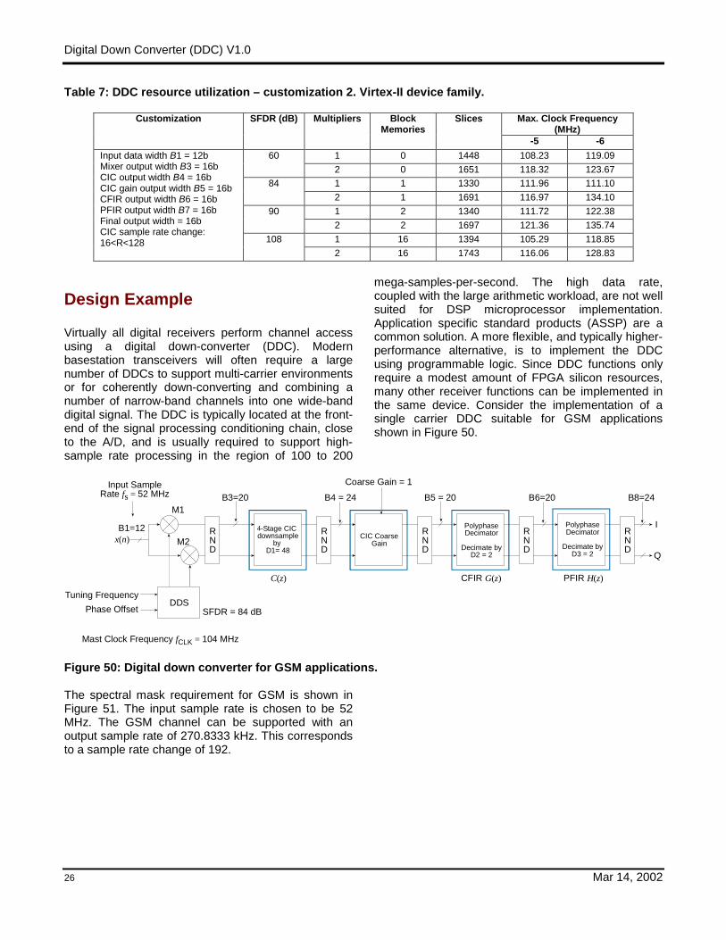
Resource Utilization
Tables 6 and 7 provide device utilization data forseveral DDC customizations implemented using theVirtex-II FPGA family. The maximum achievable clockfrequency for the particular customization is suppliedfor –5 and –6 (fastest) devices.
Table 6: DDC resource utilization – customization 1. Virtex-II device family.
Max. Clock Frequency(MHz)
Customization SFDR (dB) Multipliers BlockMemories
Slices
-5 -61 0 1611 106.86 116.0602 0 1964 109.73 123.01 1 1495 116 117.34842 1 1858 112.75 124.361 2 1502 103.81 113.02902 2 1864 108.38 120.891 16 1558 101.66 115.69
Input data width B1 = 16bMixer output width B3 = 20bCIC output width B4 = 24bCIC gain output width B5 = 20bCFIR output width B6 = 24bPFIR output width B7 = 24bFinal output width B8 = 24bCIC sample rate change:16<R<128 108
2 16 1913 110.69 124.16
Digital Down Converter (DDC) V1.0
26 Mar 14, 2002
Table 7: DDC resource utilization – customization 2. Virtex-II device family.
Max. Clock Frequency(MHz)
Customization SFDR (dB) Multipliers BlockMemories
Slices
-5 -61 0 1448 108.23 119.09602 0 1651 118.32 123.671 1 1330 111.96 111.10842 1 1691 116.97 134.101 2 1340 111.72 122.38902 2 1697 121.36 135.741 16 1394 105.29 118.85
Input data width B1 = 12bMixer output width B3 = 16bCIC output width B4 = 16bCIC gain output width B5 = 16bCFIR output width B6 = 16bPFIR output width B7 = 16bFinal output width = 16bCIC sample rate change:16<R<128 108
2 16 1743 116.06 128.83
Design Example
Virtually all digital receivers perform channel accessusing a digital down-converter (DDC). Modernbasestation transceivers will often require a largenumber of DDCs to support multi-carrier environmentsor for coherently down-converting and combining anumber of narrow-band channels into one wide-banddigital signal. The DDC is typically located at the front-end of the signal processing conditioning chain, closeto the A/D, and is usually required to support high-sample rate processing in the region of 100 to 200
mega-samples-per-second. The high data rate,coupled with the large arithmetic workload, are not wellsuited for DSP microprocessor implementation.Application specific standard products (ASSP) are acommon solution. A more flexible, and typically higher-performance alternative, is to implement the DDCusing programmable logic. Since DDC functions onlyrequire a modest amount of FPGA silicon resources,many other receiver functions can be implemented inthe same device. Consider the implementation of asingle carrier DDC suitable for GSM applicationsshown in Figure 50.
x(n)B1=12
B3=20Input Sample
Rate fs = 52 MHz
M1
M2
PolyphaseDecimator
Decimate byD2 = 2
4-Stage CIC downsample
by D1= 48
PolyphaseDecimator
Decimate byD3 = 2
C(z) CFIR G(z) PFIR H(z)
Coarse Gain = 1
DDSTuning Frequency
Phase Offset
B4 = 24 B6=20
I
B8=24
Q
SFDR = 84 dB
RND
RND
CIC CoarseGain
RND
B5 = 20
RND
RND
Mast Clock Frequency fCLK = 104 MHz
Figure 50: Digital down converter for GSM applications.
The spectral mask requirement for GSM is shown inFigure 51. The input sample rate is chosen to be 52MHz. The GSM channel can be supported with anoutput sample rate of 270.8333 kHz. This correspondsto a sample rate change of 192.

Digital Down Converter (DDC) V1.0
27 Mar 14, 2002
-500 0 500-100
-80
-60
-40
-20
0
Frequency (kHz)
DB
Figure 51: GSM spectral mask.
The baseband channel is highly oversampled so asimple cascade of boxcar filters, implemented as acascaded integrator comb (CIC) [1] will be employed
to initially reduce the sample rate by a factor of 48.The CIC filter C z( ) is multiplierless consisting only ofintegrator and differentiator sections. For thisapplication a cascade of 4 integrators followed by 4differentiators, with an embedded 48:1 rate change,will be employed. A desirable characteristic of the CICfilter in the context VLSI design is of course that it ismultiplier free. However, as described in [1], theprecision required in the integrator and differentiatorsections can be non-trivial, growing to 40-bits or more.This can potentially lead to operating speed issues insome technologies because of the serial dependencyin the adder/subtractor carry chains. Modern FPGAdevices like Virtex-II provide extremely highperformance carry chains, and even the long carry-chains that can be required in some CIC filters can besupported at very high speed.
0 0.5-150
-100
-50
0
Freq.
DB
(a) C(ejω)
0 0.5
-100
-50
0
Freq.
(b) G(ejω)
0 0.5-60
-40
-20
0
Freq. (kHz)
(c) H(ejω)
0 500-100
-50
0
Freq. (kHz)
(d) C(ejω)G(ejω)H(ejω)
Figure 52: Frequency characterizations. (a) C z( ). (b) G z( ). (c) H z( ). (d) Aggregate frequency responseand GSM spectral mask overlay.
The CIC filter is followed by a cascade of two 2:1polyphase decimators to produce the required input-to-output sample rate change of 192:1. A 21-tap filter isused for the polyphase decimator G z( ) while a 63-tapfilter is employed for H z( ). Figure 52 (a), (b) and (c)illustrate the spectral responses for the filters C z( ) ,G z( ) and H z( ) respectively. Figure 52(d) is theaggregate response, obtained by convolving theimpulse response of the three filters with each other.We observe that the combined response satisfies theGSM spectral mask requirements. Virtex-II is thetarget architecture so that the multipliers in the inputmixer will be realized using the embedded multipliers.The clock frequency for the design will be 104 MHz sothat the 2 multiplications in the mixer can be performedby a single time-shared physical multiplier.
The FPGA resource utilization data for this design isprovided in Table 8.
Table 8: GSM DDC resource utilization.FPGA Resource Number RequiredLogic Slices 1,373Embedded Multipliers 1Block RAM 1
The design was implemented in an XC2V1000bg575-5Virtex-II FPGA using the Xilinx 4.2i software tools(speed file v1.96) and easily met the required 104MHz clock frequency. The place-and-route effort levelemployed was the default value of 2 (-ol 2).
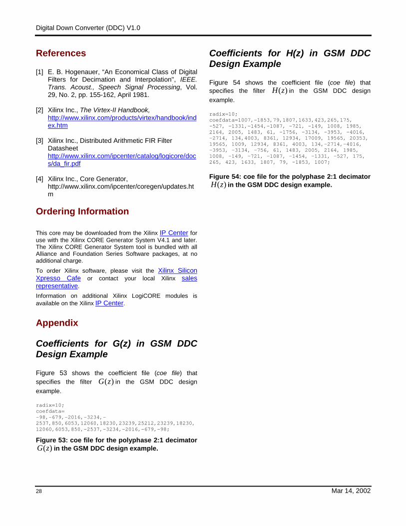
The coefficient files (coe files) that specify the filtersG z( ) and H z( ) are supplied in this document’sappendix.
Digital Down Converter (DDC) V1.0
28 Mar 14, 2002
References
[1] E. B. Hogenauer, “An Economical Class of DigitalFilters for Decimation and Interpolation'', IEEE.Trans. Acoust., Speech Signal Processing, Vol.29, No. 2, pp. 155-162, April 1981.
[2] Xilinx Inc., The Virtex-II Handbook,http://www.xilinx.com/products/virtex/handbook/index.htm
[3] Xilinx Inc., Distributed Arithmetic FIR FilterDatasheethttp://www.xilinx.com/ipcenter/catalog/logicore/docs/da_fir.pdf
[4] Xilinx Inc., Core Generator,http://www.xilinx.com/ipcenter/coregen/updates.htm
Ordering Information
This core may be downloaded from the Xilinx IP Center foruse with the Xilinx CORE Generator System V4.1 and later.The Xilinx CORE Generator System tool is bundled with allAlliance and Foundation Series Software packages, at noadditional charge.To order Xilinx software, please visit the Xilinx SiliconXpresso Cafe or contact your local Xilinx salesrepresentative.Information on additional Xilinx LogiCORE modules isavailable on the Xilinx IP Center.
Appendix
Coefficients for G(z) in GSM DDCDesign Example
Figure 53 shows the coefficient file (coe file) thatspecifies the filter ( )G z in the GSM DDC designexample.
radix=10;coefdata=-98,-679,-2016,-3234,-2537,850,6053,12060,18230,23239,25212,23239,18230,12060,6053,850,-2537,-3234,-2016,-679,-98;
Figure 53: coe file for the polyphase 2:1 decimatorG z( ) in the GSM DDC design example.
Coefficients for H(z) in GSM DDCDesign Example
Figure 54 shows the coefficient file (coe file) thatspecifies the filter H z( ) in the GSM DDC designexample.
radix=10;coefdata=1007,-1853,79,1807,1633,423,265,175,-527, -1331,-1454,-1087, -721, -149, 1008, 1985,2164, 2005, 1483, 61, -1756, -3134, -3953, -4016,-2714, 134,4003, 8361, 12934, 17009, 19565, 20353,19565, 1009, 12934, 8361, 4003, 134,-2714,-4016,-3953, -3134, -756, 61, 1483, 2005, 2164, 1985,1008, -149, -721, -1087, -1454, -1331, -527, 175,265, 423, 1633, 1807, 79, -1853, 1007;
Figure 54: coe file for the polyphase 2:1 decimatorH z( ) in the GSM DDC design example.