digital devices - vgtudspace.vgtu.lt/bitstream/1/1378/1/1336_laptik_digital_web.pdf · digital...
TRANSCRIPT

Raimond LAPTIK
DIGITAL DEVICES
Vilnius “Technika” 2012
The Essential Renewal of Undergraduates Study Programs
of VGTU Electronics Faculty
Project NoVP1-2.2-ŠMM-07-K-01-047

Raimond LAPTIK
DIGITAL DEVICES
VILNIUS GEDIMINAS TECHNICAL UNIVERSITY
Vilnius “Technika” 2012
A Laboratory Manual

R. Laptik. Digital Devices: A Laboratory Manual. Vilnius: Technika, 2012. 133 p. [4,35 author’s sheets, 2012 06 04].
The goal of this manual for laboratory works is to provide means for students to prepare for laboratory works in the subject of digital devices. The manual is for the Faculty of Electronics of VGTU, study programs in electronics engineering, automation, telecommunications engineering, computer engineering, informa-tion systems engineering. The main topics are: number systems and binary codes; simulation software EWB and Multisim; basic logic gates; minimization of logic functions; TTL, CMOS and BiCMOS switches; design of arithmetic and combi-national logic devices; combinational logic IC devices; basic latches, registers and counters. Each work is presented with objectives, short theory and methodology, example of the task and control questions to check mastering of the theory.
The publication has been recommended by the Study Committee of VGTU Electronics Faculty.
Reviewed by:Prof Habil Dr Raimundas Kirvaitis, VGTU Department of Electronic Systems,Prof Habil Dr Vygaudas Kvedaras, VGTU Department of Electrical Engineering
This publication has been produced with the financial assistance of Europe Social Fund and VGTU (Project No VP1-2.2-ŠMM-07-K-01-047). The book is a part of the project “The Essential Renewal of Undergraduates Study Programs of VGTU Electronics Faculty”.
This is an educational methodology book, No 1336-S, issued by VGTU Press TECHNIKA http://leidykla.vgtu.lt
Language editor Vida BėkštienėTypesetter Laura Petrauskienė
eISBN 978-609-457-159-6doi:10.3846/1336-S
© Raimond Laptik, 2012© Vilnius Gediminas Technical University, 2012

3
Contents
Introduction . . . . . . . . . . . . . . . . . . . . . . . . . . . . 41. Introduction into number systems and binary codes . . . . . . 52. EWB and Multisim. Basic logic gates . . . . . . . . . . . . .193. Minimization of logic functions . . . . . . . . . . . . . . . .304. Algebraic minimization of logic functions . . . . . . . . . . .385. BJT switch. Investigation of RTL and DTL gates . . . . . . .436. Investigation of Standard TTL gate . . . . . . . . . . . . . .517. Investigation of MOS and CMOS switches . . . . . . . . . .588. Investigation of BICMOS switch . . . . . . . . . . . . . . . .669. Design of arithmetic devices . . . . . . . . . . . . . . . . . .7510. Gate level design of other combinational logic devices . . . .8511. Combinational logic IC devices . . . . . . . . . . . . . . . .9812. Basic synchronous latches . . . . . . . . . . . . . . . . . 10613. Registers . . . . . . . . . . . . . . . . . . . . . . . . . . . 11714. Counters . . . . . . . . . . . . . . . . . . . . . . . . . . . 123References . . . . . . . . . . . . . . . . . . . . . . . . . . . . 133

4
intRoDuCtion
the goal of this manual for laboratory works is to provide means for students to prepare for laboratory works in the subject of digital devices.
each work is presented with objectives, short theory, methodol-ogy, example of the task and control questions to check mastering of the theory. At the end of each work the literature is presented where the student can get more information regarding the subject. during the laboratory work the tutor presents an individual task for each student. each task consists of two parts. the main part is obligatory and should be fulfilled before starting the additional part. The maxi-mum evaluation of the main part is 6 points, and the maximum eval-uation of the additional part is 4 points. in the majority of the tasks students will design various digital circuits. electronics Workbench and multisim software packages are used for circuit simulation, so the student has the opportunity to check the operation of the circuit designed and to show the operation of the circuit to the tutor.

5
1. intRoDuCtion into numbeR systems anD binaRy CoDes
objectives of the Work
the goal of this introduction is to provide the basic theory for students to get acquainted with different positional number systems and binary codes and to be able to perform simple arithmetical ope-rations in various number systems.
theory
introduction
it is crucial to understand composition of number systems and binary codes because the subject of digital devices is based on this knowledge.
the majority of number systems are positional. in positional number system, the base of the system and position of digit or sym-bol of this number system together determine the final value of the number. the most popular number system is decimal. it is called decimal because of ten symbols from “0” to “9” which are used to represent one position of a multipositional number. the number of symbols used to represent one position is called the base B or radix of the system and is usually indicated by a subscript. the position of a symbol in a number determines value of the symbol. in decimal system 10B = and every position in the number has the value of 10 in power n, where n is a position calculated from the radix point. Values of positions in decimal system are presented in table 1.1.

6
table 1.1 Values of positions in decimal system
Position 4 3 2 1 0. –1 –2 –3
Value410 310 210 110 010 110− 210− 310−
10000 1000 100 10 1 0.1 0.01 0.001
With each position to the left, value of position increases 10 times, with each position to the right value of position decreases 10 times.
so to the left of the radix point in decimal system there is the position of ones, the position of tens, then hundreds and so on. to the right of the radix point there is the position of tenths, the position of hundredths and so on.
the same rules are applied to every positional number system.An infinite number of positional number systems exists with
base B, however the most popular are binary, octal, decimal and hexadecimal systems.
binary system
in conventional arithmetic, number system based on ten sym-bols is used. however, digital circuits used in computers and other digital systems usually operate with two distinct voltage levels, ex-pressed as 0’s and 1’s. number system with the basic symbols “0” and “1” is called binary and it’s base is 2B = . Values of positions of bits in binary system are presented in table 1.2.
table 1.2 Values of positions in binary system
Position 4 3 2 1 0. –1 –2 –3
Value42 32 22 12 02 12− 22− 32−
16 8 4 2 1 0.5 0.25 0.125

7
example of conversion from the binary system to decimal:
2 1 0 1 22
10
110.01 1 2 1 2 0 2 0 2 1 24 2 0 0 0.25 6.25
− −= × + × + × + × + ×= + + + + =
(1.1)
conversion is performed by multiplying the symbol of each po-sition by the base raised into the power of position.
conversion from decimal system to binary is a little bit more complicated as it requires division of the integer part and multiplica-tion of the fractional, thus both parts should be converted separately and then added. example of conversion from decimal to binary is shown in Fig. 1.1. At first the number is divided into integer and fractional parts. then integer part is continuously divided by the base transferring the result into dividend for the next division until the result is zero. the remainder of the division is taken as a result-ing digit for one position of binary system. the binary number is filled with values starting from the right so, that the first remainder will be the rightmost digit. in the case of fractional part, the number is being multiplied by a base and the first integer part of the result is written into the leftmost position. the result without the integer part is taken as the multiplicand for the next multiplication. multi-plication is continued until the result is zero, or in the case of infi-nite fraction, until the required precision is reached. Infinite frac-tion is indicated by a repeating sequence of numbers. For example:
10 20.3 0.0 1001 1001...= or 10 20.7 0.1 0110 0110...= .

8
10
10 2 2 2
6.25 6 0.25
6 / 2 3, remainder 03 / 2 1, remainder 11 / 2 0, remainder 10 / 2 0, stop
6.25 1 1 0 .0 1 110.01
0.25 2 0.5, integer part 00.5 2 1.0, integer part 10.0 2 0.0, stop
= +
====
= + =
× =× =× =
Fig. 1.1 decimal to binary conversion
octal system
Octal number system with the base 8B = is using eight sym-bols from “0” to “7” to express the value of one position.
table 1.3 Values of positions in octal system
Position 4 3 2 1 0. –1 –2
Value48 38 28 18 08 18− 28−
4096 512 64 8 1 0.125 0.015625
conversion from octal to decimal is performed in a similar way as from binary to decimal:

9
2 1 0 1 28
10
371.51 3 8 7 8 1 8 5 8 1 8192 56 1 0.625 0.015625 249.640625
− −= × + × + × + × + ×
= + + + + =
(1.2)
conversion from decimal to octal system is also performed via the division of the integer part and multiplication of the fractional part (Fig. 1.2).
10
10 8 8 8
26.25 26 0.25
26 / 8 3, remainder 23 / 8 0, remainder 30 / 8 0, stop
26.25 32 .2 32.2
0.25 8 2.0, integer part 20.0 8 0.0, stop
= +
===
= + =
× =× =
Fig. 1.2 decimal to octal conversion
Octal number system is less frequently used than binary or hexadecimal, however it is still popular because of the ease of the conversion from binary to octal system and vice versa. in general all number systems could be easily converted if the base of one system could be expressed as the base of other system raised to the integer power. And the exponent will point how many positions are needed in the other system to express one position in the current system. For example, the relation of the bases of octal and binary systems is 1 38 2= , so one position in octal system will take three positions

10
in binary system. Again, the position is calculated from the radix point. this could be used for direct conversion:
9
Octal number system is less frequently used than binary or hex-adecimal, however it is still popular because of the ease of the con-version from binary to octal system and vice versa. in general all number systems could be easily converted if the base of one system could be expressed as a base of other system raised to the integer power. And the exponent will point how many positions are needed in the other system to express one position in the current system. For example the relation of the bases of octal and binary systems is
1 38 2= , so one position in octal system will take three positions in binary system. Again, the position is calculated from the radix point. this could be used for direct conversion:
2 87 42 6 0 1 . 6
8 2010 001 100110 111 000 . 110
10110111000001 . 1101 26701.64
2 6 7 0 1 . 6 4 010110111000001.110100
=
=(1.3)
Hexadecimal system
hexadecimal system is quite often used to express binary num-bers in a more readable form as hexadecimal number is usually four times shorter than binary. hexadecimal system with the base 16B =is using 16 different symbols from “0” to “F” (numbers from 0 to 9 and letters from A to F) to express the values from 0 to 15.
table 1.4 the values of positions in hexadecimal system
Position 3 2 1 0. –1 –2
Value 316 216 116 016 116− 216−
4096 256 16 1 0.0625 0.00390625
conversion from hexadecimal system to decimal is performed in a similar way as from binary to decimal:
(1.3)
Hexadecimal system
hexadecimal system is quite often used to express binary num-bers in a more readable form as hexadecimal number is usually four times shorter than binary. hexadecimal system with base 16B = is using 16 different symbols from “0” to “F” (numbers from 0 to 9 and letters from A to F) to express values from 0 to 15.
table 1.4 Values of positions in hexadecimal system
Position 3 2 1 0. –1 –2
Value316 216 116 016 116− 216−
4096 256 16 1 0.0625 0.00390625
conversion from hexadecimal system to decimal is performed in a similar way as from binary to decimal:
2 1 0 1 216
2 1 0 1 2
10
B3F.A1 B 16 3 16 F 16 A 16 1 16
11 16 3 16 15 16 10 16 1 162816 48 15 0.625 0.003906252879.62890625
− −
− −
= × + × + × + × + ×
= × + × + × + × + ×= + + + +=
(1.4)
conversion from decimal to hexadecimal is the same as in the majority of positional number systems (Fig. 1.3).
11
10
10 16 16
2879.62890625 2879 0.62890625
2879 /16 179, remainder 15 F179 /16 11, remainder 311/16 0, remainder 11 B0 /16 0, stop
2879.62890625 B 3 F .A 1
= +
= →== →=
= +
16 B3F.A1
0.62890625 16 10.0625, integer part 10 A0.0625 16 1.0, integer part 1
0.0 16 0.0, stop
=
× = →× =
× =
Fig. 1.3 decimal to hexadecimal conversion
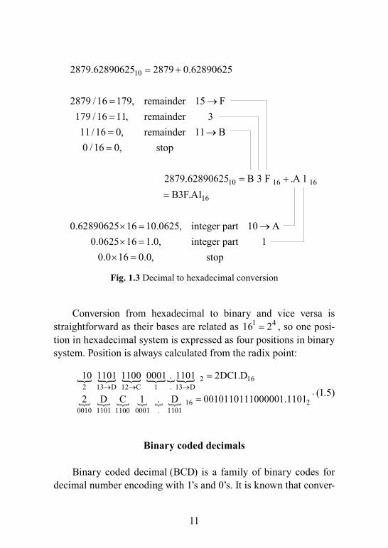
conversion from hexadecimal to binary and vice versa is straightforward as their bases are related as 1 416 2= , so one posi-tion in hexadecimal system is expressed as four positions in binary system. Position is always calculated from the radix point:
10
2 1 0 1 216
2 1 0 1 2
10
B3F.A1 B 16 3 16 F 16 A 16 1 16
11 16 3 16 15 16 10 16 1 162816 48 15 0.625 0.003906252879.62890625
− −
− −
= × + × + × + × + ×
= × + × + × + × + ×= + + + +=
. (1.4)
conversion from decimal to hexadecimal is the same as in ma-jority of positional number systems (Fig. 1.3).
10
10 16 16
2879.62890625 2879 0.62890625
2879 /16 179, remainder 15 F179 /16 11, remainder 311/16 0, remainder 11 B0 /16 0, stop
2879.62890625 B 3 F .A 1
= +
= →== →=
= +
16 B3F.A1
0.62890625 16 10.0625, integer part 10 A0.0625 16 1.0, integer part 1
0.0 16 0.0, stop
=
× = →× =
× =
Fig. 1.3 decimal to hexadecimal conversion
conversion from hexadecimal to binary and vice versa is straightforward as their bases are related as 1 416 2= , so one position in hexadecimal system is expressed as four positions in binary sys-tem. Position is always calculated from the radix point:
2 162 13 d 12 c 1 . 13 d
16 20010 1101 0001 11011100 .
10 1101 1100 0001 . 1101 2dc1.d
2 d c 1 . d 0010110111000001.1101→ → →
=
=. (1.5) (1.5)
binary coded decimals
Binary coded decimal (Bcd) is a family of binary codes for decimal number encoding with 1’s and 0’s. it is known that conver-
12
sion between decimal and binary numbers requires a lot of calcu-lations. In BCD code a fixed number of bits is used to encode one position of decimal number. Also when Bcd code is used its name is indicated by a subscript and the name of the code usually consists of the weights for each position of the bit:
11
binary coded decimals
Binary coded decimal (Bcd) is a family of binary codes for dec-imal number encoding with 1’s and 0’s. it is known that conversion between decimal and binary numbers requires a lot of calculations. in Bcd code a fixed number of bits is used to encode one position of decimal number. Also when Bcd code is used its name is indicated by a subscript and the name of the code usually consists of the weights for each position of the bit:
Bcd8421 107 4 2 1 9 8 1 5 4 1 3 2 1
Bcd4221 105 2 2 1 5 4 1 3 2 1 3 2 1
10 Bcd84210010 01000110 1000
00101010
0111 1001 0101 0011 7953
0111 1001 0101 0011 5533
6 2 8 4 0110 0010 1000 0100
6 2 8
= + + = + = + = +
= + + = + = + = +
=
=
=
10 Bcd422101101110
4 1010 0010 1110 0110=
. (1.6)
Gray code
Gray code is a cyclic binary code where only one bit is changing when the number is increased or decreased. such code is used in the circuits where the fluctuation of the voltage is not desirable. For ex-ample the counter output is connected to the wide bus and if binary system is used then when an overflow occurs and the counting starts from 0 there is an impact on the bus voltage, when a lot of bits are switched at the same time. On the contrary, when Gray code is used, only one bit will change during overflow.
conversion from binary system to Gray code is performed via XOr (exclusive Or) operation. XOr operation, denoted with “⊕ “ symbol, is pointing if two bits are different or not. if two bits are different, then the result is 1, if two bits are the same then the result is 0. during the first step, the most significant bit (one from the left) is written down (Fig. 1.4 a), next the XOr operation is performed with the bit to the right and the result is written into the next free
(1.6)
Gray code
Gray code is a cyclic binary code where only one bit is chang-ing when the number is increased or decreased. such code is used in the circuits where fluctuation of the voltage is not desirable. For example, the counter output is connected to the wide bus and if bi-nary system is used then, when an overflow occurs and the counting starts from 0, there is an impact on the bus voltage, when a lot of bits are switched at the same time. On the contrary, when Gray code is used, only one bit will change during overflow.
conversion from binary system to Gray code is performed via XOr (exclusive Or) operation. XOr operation, denoted with “ ⊕ “ symbol, is pointing if two bits are different or not. if two bits are different, then the result is 1, if two bits are the same then the result is 0. During the first step, the most significant bit (one from the left) is written down (Fig. 1.4 a), next XOr operation is performed with the bit to the right and the result is written into the next free position (Fig. 1.4 b). this step is repeated until all the bits are converted.
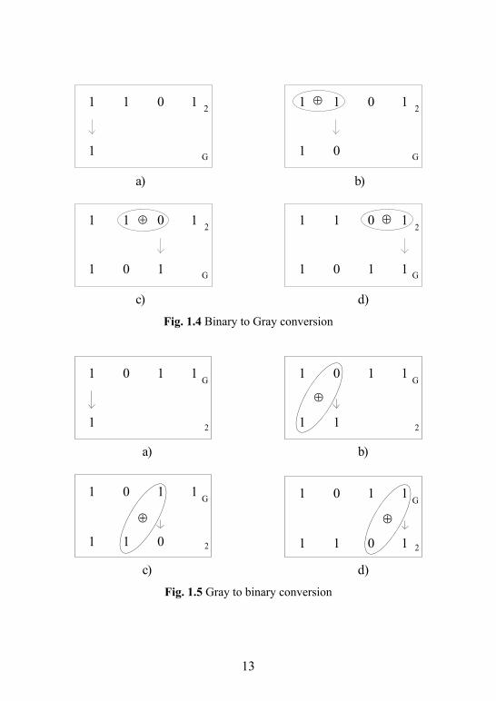
13
a)
1 1 0 1
1
2
G
b)
1 1 0 1
1 0
2
G
⊕
c)
1 1 0 1
1 0 1
2
G
⊕
d)
1 1 0 1
1 0 1 1
2
G
⊕
Fig. 1.4 Binary to Gray conversion
a)
1 0 1 1
1 2
G
b)
1 0 1 1
1 1 2
G
⊕
c)
1 0 1 1
1 1 0 2
G
⊕
d)
1 0 1 1
1 1 0 1 2
G
⊕
Fig. 1.5 Gray to binary conversion

14
in the similar way the conversion from Gray code to binary system is done (Fig. 1.5). The first step is exactly the same – the left bit is written down. next XOr operation is performed between the written down bit and the next bit in Gray code and the result is writ-ten into the next free position. XOr operation is repeated until all the bits are calculated.
The reflective property of Gray code (Fig. 1.6) could be used to generate a sequential set of numbers by reflecting the leftmost position every 12 bits, the second position every 22 bits, the third position every 32 and so on.
0 0 0
0 0 1
0 1 1
0 1 0
1 1 0
1 1 1
1 0 1
1 0 0 Fig. 1.6 Reflective property of Gray code
arithmetical operations
in the majority of positional number systems arithmetical ope-rations are performed in the same way as in decimal system. in addition and subtraction numbers should be aligned relative to the radix point. Position of the radix point is static (does not change) in addition and subtraction. however in multiplication alignment of numbers is not necessary, as the position of the radix point in the result should be recalculated according to the sum of positions in the fractional parts of the numbers being multiplied.

15
In addition when there is an overflow in one position the value is being carried into another position to the left, in the same way as it is done in decimal system. example of binary addition is pro-vided:
1 1 11 1 1 1
2 2 2
2 2 2
2 2 2
101 110100 1101.01 10 110101 11.11
111 1101001 10001.00
+ + + (1.7)
Overflow in octal system happens when the sum of digits is 8 or greater. Addition in octal number system:
1 1 1 1 1 1 1
8 8 8
8 8 8
8 8 8
301 170153 1711.62 17 670644 71.53
320 1061017 2003.35
+ + + (1.8)
In hexadecimal system the overflow happens when the sum is 16 or greater:
1 1 1 1
16 16 16
16 16 16
16 16 16
37A F70153 1751.A 2 9 1 640F4e 71.B3
40B 15B10A1 17c3.55
+ + + (1.9)
subtraction is also performed in a similar way as in decimal system. During the underflow, the borrowing should be done from the next position to the left, if that position is empty then the next one is considered. the borrowed unit from the left position is expressed as B units in the current position. in the case of binary subtraction
2B = and the borrowed unit from the left is transformed into exactly two units in the current position:
16
14
1 1 11 1 1 1
2 2 2
2 2 2
2 2 2
101 110100 1101.01 10 110101 11.11
111 1101001 10001.00
+ + +. (1.7)
Overflow in octal system happens when the sum of digits is 8 or greater. Addition in octal number system:
1 1 1 1 1 1 1
8 8 8
8 8 8
8 8 8
301 170153 1711.62 17 670644 71.53
320 1061017 2003.35
+ + +. (1.8)
in hexadecimal system the overflow happens when the sum is 16 or greater:
1 1 1 1
16 16 16
16 16 16
16 16 16
37 A F70153 1751.A 2 9 1 640F4e 71.B3
40B 15B10A1 17c3.55
+ + +. (1.9)
subtraction is also performed in a similar way as in the decimal system. during the underflow, the borrowing should be done from the next position to the left, if that position is empty then the next one is considered. Borrowed unit from the left position is expressed as B units in the current position. in the case of binary subtraction
2B = and borrowed unit from the left is transformed into exactly two units in the current position:
11 1 1
1 1 1 122 2
2 2 2
2 2 2
111 110100 1101.01 10 10001 11.11
101 100011 1001.10
− − −
i i i
. (1.10)
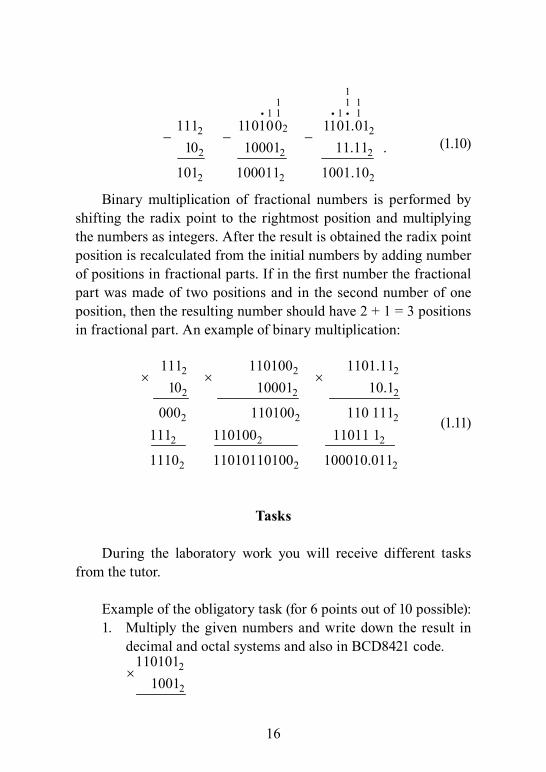
Binary multiplication of fractional numbers is performed by shifting the radix point to the rightmost position and multiplying the
(1.10)
Binary multiplication of fractional numbers is performed by shifting the radix point to the rightmost position and multiplying the numbers as integers. After the result is obtained the radix point position is recalculated from the initial numbers by adding number of positions in fractional parts. If in the first number the fractional part was made of two positions and in the second number of one position, then the resulting number should have 2 + 1 = 3 positions in fractional part. An example of binary multiplication:
2 2 2
2 2 2
2 2 2
2 2 2
2 2 2
111 110100 1101.11 10 10001 10.1
000 110100 110 111111 110100 11011 1
1110 11010110100 100010.011
× × ×
(1.11)
tasks
during the laboratory work you will receive different tasks from the tutor.
example of the obligatory task (for 6 points out of 10 possible):1. multiply the given numbers and write down the result in
decimal and octal systems and also in Bcd8421 code.2
2
110101 1001
×

17
example of the additional tasks (2 points each):2. convert the binary number 21010.011 into decimal. 3. From 1011 students 22 are female and 212 are male.
What is the base of the system used? (All the numbers are in the same system).
Control questions
1. convert these binary numbers 101101; 10; 110.01 into deci-mal system.
2. convert these octal numbers 7501; 10; 15.4 into decimal system.
3. convert these hexadecimal numbers A1F; 10; B.A into dec-imal system.
4. convert these decimal numbers 1458; 19; 78.25 into binary, octal and hexadecimal number systems.
5. Perform direct conversion of binary number 10101110101 into octal and hexadecimal number systems.
6. convert these octal numbers 1234; 32; 12.5 into hexadeci-mal number system.
7. convert these decimal numbers 14; 1587; 355 into Bcd8421 code.
8. convert binary number 10011 into Gray code.9. Add these binary numbers: 101011101 and 10111.1.10. subtract these binary numbers: 100010 and 10111.1.11. multiply these binary numbers: 101011.1 and 101.01.12. multiply these binary numbers: 0.0001 and 10000.
Literature
1. Kleitz, W. (2008). Digital Electronics: A Practical Ap-proach. mcGraw hill, p. 2–19.

18
2. lala, Parag, K. (2007). Principles of Modern Digital De-sign. A John Willey & sons inc., p. 1–27.
3. Kirvaitis, r. (2000). Digital Devices. E-Text-book. Avail-able from the author, p. 4–12.
4. Kirvaitis, r. (1999). Loginės schemos. Vilnius: enciklope-dija, p. 21–31. (in lithuanian)
19
2. eWb anD muLtisim. basiC LoGiC Gates
objective
the goal of this work is: to get acquainted with the digital cir-cuits’ simulation software; to get the basic understanding of the logic gates and their conversion; to be able to fill the truth table and design a simple circuit implementing the logic function.
theory
eWb and multisim
in the laboratory you will use one of the two simulation soft-ware packages: electronics Workbench or multisim, which is the newer version of electronics Workbench with wider functionality. Both of them are suitable for simulation of digital circuits and pro-vide all the necessary tools for analysis of digital devices. however the older electronics Workbench is simpler for application and its functionality is more than sufficient for laboratory works.
using these packages you can design a circuit from the basic logic gates and perform its simulation using logic Analyzer with Word Generator or logic converter tools.
basic logic functions and gates
three main logic functions And, Or and nOt may be real-ized with corresponding logic gate. in the case of the logic function, Boolean algebra notation is used, where 0 means low level or false, 1 means high level or true. Because of the manufacturing processes the integrated digital circuits usually are made from nAnd or from
20
nOr logic gates. using nAnd gates only or nOr gates only it is possible to realize every logic expression or design of any digital device.
table 2.1 Basic logic gates
name Graphical symbol
logic function truth table
anD
18
Table 2.1 Basic logic gates
Name Graphical symbol Logic function Truth table
AND &A
BF
F = AB A B F 0 0 0 0 1 0 1 0 0 1 1 1
OR 1A
BF
F = A+ B A B F 0 0 0 0 1 1 1 0 1 1 1 1
XOR 1A
BF
F = A B A B F 0 0 0 0 1 1 1 0 1 1 1 0
NAND &A
BF
F = AB A B F 0 0 1 0 1 1 1 0 1 1 1 0
NOR 1A
BF
F = A+ B A B F 0 0 1 0 1 0 1 0 0 1 1 0
XNOR 1A
BF
F = A B A B F 0 0 1 0 1 0 1 0 0 1 1 1
NOTInverter 1A F F = A A F
0 1 1 0
F = AB
18
Table 2.1 Basic logic gates
Name Graphical symbol Logic function Truth table
AND &A
BF
F = AB A B F 0 0 0 0 1 0 1 0 0 1 1 1
OR 1A
BF
F = A+ B A B F 0 0 0 0 1 1 1 0 1 1 1 1
XOR 1A
BF
F = A B A B F 0 0 0 0 1 1 1 0 1 1 1 0
NAND &A
BF
F = AB A B F 0 0 1 0 1 1 1 0 1 1 1 0
NOR 1A
BF
F = A+ B A B F 0 0 1 0 1 0 1 0 0 1 1 0
XNOR 1A
BF
F = A B A B F 0 0 1 0 1 0 1 0 0 1 1 1
NOTInverter 1A F F = A A F
0 1 1 0
oR
18
Table 2.1 Basic logic gates
Name Graphical symbol Logic function Truth table
AND &A
BF
F = AB A B F 0 0 0 0 1 0 1 0 0 1 1 1
OR 1A
BF
F = A+ B A B F 0 0 0 0 1 1 1 0 1 1 1 1
XOR 1A
BF
F = A B A B F 0 0 0 0 1 1 1 0 1 1 1 0
NAND &A
BF
F = AB A B F 0 0 1 0 1 1 1 0 1 1 1 0
NOR 1A
BF
F = A+ B A B F 0 0 1 0 1 0 1 0 0 1 1 0
XNOR 1A
BF
F = A B A B F 0 0 1 0 1 0 1 0 0 1 1 1
NOTInverter 1A F F = A A F
0 1 1 0
F = A+ B
18
Table 2.1 Basic logic gates
Name Graphical symbol Logic function Truth table
AND &A
BF
F = AB A B F 0 0 0 0 1 0 1 0 0 1 1 1
OR 1A
BF
F = A+ B A B F 0 0 0 0 1 1 1 0 1 1 1 1
XOR 1A
BF
F = A B A B F 0 0 0 0 1 1 1 0 1 1 1 0
NAND &A
BF
F = AB A B F 0 0 1 0 1 1 1 0 1 1 1 0
NOR 1A
BF
F = A+ B A B F 0 0 1 0 1 0 1 0 0 1 1 0
XNOR 1A
BF
F = A B A B F 0 0 1 0 1 0 1 0 0 1 1 1
NOTInverter 1A F F = A A F
0 1 1 0
XoR
18
Table 2.1 Basic logic gates
Name Graphical symbol Logic function Truth table
AND &A
BF
F = AB A B F 0 0 0 0 1 0 1 0 0 1 1 1
OR 1A
BF
F = A+ B A B F 0 0 0 0 1 1 1 0 1 1 1 1
XOR 1A
BF
F = A B A B F 0 0 0 0 1 1 1 0 1 1 1 0
NAND &A
BF
F = AB A B F 0 0 1 0 1 1 1 0 1 1 1 0
NOR 1A
BF
F = A+ B A B F 0 0 1 0 1 0 1 0 0 1 1 0
XNOR 1A
BF
F = A B A B F 0 0 1 0 1 0 1 0 0 1 1 1
NOTInverter 1A F F = A A F
0 1 1 0
F = A B⊕
18
Table 2.1 Basic logic gates
Name Graphical symbol Logic function Truth table
AND &A
BF
F = AB A B F 0 0 0 0 1 0 1 0 0 1 1 1
OR 1A
BF
F = A+ B A B F 0 0 0 0 1 1 1 0 1 1 1 1
XOR 1A
BF
F = A B A B F 0 0 0 0 1 1 1 0 1 1 1 0
NAND &A
BF
F = AB A B F 0 0 1 0 1 1 1 0 1 1 1 0
NOR 1A
BF
F = A+ B A B F 0 0 1 0 1 0 1 0 0 1 1 0
XNOR 1A
BF
F = A B A B F 0 0 1 0 1 0 1 0 0 1 1 1
NOTInverter 1A F F = A A F
0 1 1 0
nanD
18
Table 2.1 Basic logic gates
Name Graphical symbol Logic function Truth table
AND &A
BF
F = AB A B F 0 0 0 0 1 0 1 0 0 1 1 1
OR 1A
BF
F = A+ B A B F 0 0 0 0 1 1 1 0 1 1 1 1
XOR 1A
BF
F = A B A B F 0 0 0 0 1 1 1 0 1 1 1 0
NAND &A
BF
F = AB A B F 0 0 1 0 1 1 1 0 1 1 1 0
NOR 1A
BF
F = A+ B A B F 0 0 1 0 1 0 1 0 0 1 1 0
XNOR 1A
BF
F = A B A B F 0 0 1 0 1 0 1 0 0 1 1 1
NOTInverter 1A F F = A A F
0 1 1 0
F = AB
18
Table 2.1 Basic logic gates
Name Graphical symbol Logic function Truth table
AND &A
BF
F = AB A B F 0 0 0 0 1 0 1 0 0 1 1 1
OR 1A
BF
F = A+ B A B F 0 0 0 0 1 1 1 0 1 1 1 1
XOR 1A
BF
F = A B A B F 0 0 0 0 1 1 1 0 1 1 1 0
NAND &A
BF
F = AB A B F 0 0 1 0 1 1 1 0 1 1 1 0
NOR 1A
BF
F = A+ B A B F 0 0 1 0 1 0 1 0 0 1 1 0
XNOR 1A
BF
F = A B A B F 0 0 1 0 1 0 1 0 0 1 1 1
NOTInverter 1A F F = A A F
0 1 1 0
noR
18
Table 2.1 Basic logic gates
Name Graphical symbol Logic function Truth table
AND &A
BF
F = AB A B F 0 0 0 0 1 0 1 0 0 1 1 1
OR 1A
BF
F = A+ B A B F 0 0 0 0 1 1 1 0 1 1 1 1
XOR 1A
BF
F = A B A B F 0 0 0 0 1 1 1 0 1 1 1 0
NAND &A
BF
F = AB A B F 0 0 1 0 1 1 1 0 1 1 1 0
NOR 1A
BF
F = A+ B A B F 0 0 1 0 1 0 1 0 0 1 1 0
XNOR 1A
BF
F = A B A B F 0 0 1 0 1 0 1 0 0 1 1 1
NOTInverter 1A F F = A A F
0 1 1 0
F = A+ B
18
Table 2.1 Basic logic gates
Name Graphical symbol Logic function Truth table
AND &A
BF
F = AB A B F 0 0 0 0 1 0 1 0 0 1 1 1
OR 1A
BF
F = A+ B A B F 0 0 0 0 1 1 1 0 1 1 1 1
XOR 1A
BF
F = A B A B F 0 0 0 0 1 1 1 0 1 1 1 0
NAND &A
BF
F = AB A B F 0 0 1 0 1 1 1 0 1 1 1 0
NOR 1A
BF
F = A+ B A B F 0 0 1 0 1 0 1 0 0 1 1 0
XNOR 1A
BF
F = A B A B F 0 0 1 0 1 0 1 0 0 1 1 1
NOTInverter 1A F F = A A F
0 1 1 0

21
XnoR
18
Table 2.1 Basic logic gates
Name Graphical symbol Logic function Truth table
AND &A
BF
F = AB A B F 0 0 0 0 1 0 1 0 0 1 1 1
OR 1A
BF
F = A+ B A B F 0 0 0 0 1 1 1 0 1 1 1 1
XOR 1A
BF
F = A B A B F 0 0 0 0 1 1 1 0 1 1 1 0
NAND &A
BF
F = AB A B F 0 0 1 0 1 1 1 0 1 1 1 0
NOR 1A
BF
F = A+ B A B F 0 0 1 0 1 0 1 0 0 1 1 0
XNOR 1A
BF
F = A B A B F 0 0 1 0 1 0 1 0 0 1 1 1
NOTInverter 1A F F = A A F
0 1 1 0
F = A B⊕
18
Table 2.1 Basic logic gates
Name Graphical symbol Logic function Truth table
AND &A
BF
F = AB A B F 0 0 0 0 1 0 1 0 0 1 1 1
OR 1A
BF
F = A+ B A B F 0 0 0 0 1 1 1 0 1 1 1 1
XOR 1A
BF
F = A B A B F 0 0 0 0 1 1 1 0 1 1 1 0
NAND &A
BF
F = AB A B F 0 0 1 0 1 1 1 0 1 1 1 0
NOR 1A
BF
F = A+ B A B F 0 0 1 0 1 0 1 0 0 1 1 0
XNOR 1A
BF
F = A B A B F 0 0 1 0 1 0 1 0 0 1 1 1
NOTInverter 1A F F = A A F
0 1 1 0
notinverter
18
Table 2.1 Basic logic gates
Name Graphical symbol Logic function Truth table
AND &A
BF
F = AB A B F 0 0 0 0 1 0 1 0 0 1 1 1
OR 1A
BF
F = A+ B A B F 0 0 0 0 1 1 1 0 1 1 1 1
XOR 1A
BF
F = A B A B F 0 0 0 0 1 1 1 0 1 1 1 0
NAND &A
BF
F = AB A B F 0 0 1 0 1 1 1 0 1 1 1 0
NOR 1A
BF
F = A+ B A B F 0 0 1 0 1 0 1 0 0 1 1 0
XNOR 1A
BF
F = A B A B F 0 0 1 0 1 0 1 0 0 1 1 1
NOTInverter 1A F F = A A F
0 1 1 0
F = A
18
Table 2.1 Basic logic gates
Name Graphical symbol Logic function Truth table
AND &A
BF
F = AB A B F 0 0 0 0 1 0 1 0 0 1 1 1
OR 1A
BF
F = A+ B A B F 0 0 0 0 1 1 1 0 1 1 1 1
XOR 1A
BF
F = A B A B F 0 0 0 0 1 1 1 0 1 1 1 0
NAND &A
BF
F = AB A B F 0 0 1 0 1 1 1 0 1 1 1 0
NOR 1A
BF
F = A+ B A B F 0 0 1 0 1 0 1 0 0 1 1 0
XNOR 1A
BF
F = A B A B F 0 0 1 0 1 0 1 0 0 1 1 1
NOTInverter 1A F F = A A F
0 1 1 0
table 2.1 represents all types of the basic logic gates together with their european graphical representation, expressions of logic functions they realize, and truth tables of these logic functions.
methodology
in the electronics Workbench you can click on an element or tool and drag it onto workspace. the properties of an element or tool could be changed by double-clicking the element or tool. short help could be received by clicking the element and pressing F1. elements and tools could be interconnected by simply clicking one of the pins of one element or tool and dragging the wire to the other pin of ele-ment or tool. For accurate connection the use of zoom function is recommended (150–200 %). disconnection of wires is possible by dragging the end of the wire from the node or pin. Wires, elements or tools can be deleted by the selection of the wire, element or tool and pressing “del” button on the keyboard.
indicators are accessible by clicking “indicators” icon on the toolbar (Fig. 2.1 a). indicators are used to display information. the most common indicators used during the laboratory works are volt-meters, ammeters, red probes and seven segment displays that de-code binary to hexadecimal.

22
tools for analysis of circuits are accessible from toolbar “in-struments” (Fig. 2.1 b). the most common tools used are oscillo-scope, logic converter, word generator and logic analyzer.
logic gates are accessible from “logic gates” toolbar (Fig. 2.1 c).
useful elements as power supplies and switches are accessible from “sources” and “Basic” toolbars.
this is not the full list of toolbars available in electronics Workbench environment. There exists toolbars dedicated to specific items as diodes, transistors, analogue integrated circuits, digital in-tegrated circuits, mixed integrated circuits, flip-flops and other mis-cellaneous items.
a)
b)
c) Fig. 2.1 toolbars of electronics Workbench 5
the use of word generator, logic analyzer and logic converter tools requires some explanation.
By double clicking the word generator tool on the workspace, the window with tool properties will open (Fig. 2.2). Word gene-
23
rator is a tool for generating various combinations of digital signals. in the left column of word generator user has a possibility to write code in hexadecimal form and by clicking “step” button each line of hexadecimal code (one word) will be decoded into the binary and supplied via the outputs row of word generator. sixteen outputs for sixteen bits are placed at the bottom of the word generator and in Electronics Workbench version 5, the least significant bit gener-ated is from the right side, so usually the connection of the circuit starts from the right. It is possible to automatically fill the word generator with a sequence of numbers by pressing “Pattern” button and then choosing one from the list. the most common pattern is “up counter”. “cycle” button will be generating sequence of words continuously, after the last word in the sequence the generation will start from the beginning. “Burst” button will generate all the words in the sequence once. to pause and restart the stream of words at a specified word is possible by clicking the “Breakpoint” button.
Fig. 2.2 Word generator tool

24
Fig. 2.3 logic analyzer tool
logic analyzer (Fig. 2.3) is often used together with word ge-nerator and is used to display changes of logic levels on time axis. the only important property of the logic analyzer is the “clocks per division” variable, by increasing this number you can compress time axis and make the plot more readable. logic analyzer has a column of 16 inputs on the left side. input signal is being plot in the logic analyzer window at the row related to the input. By changing the color of the wire (property accessible through double-clicking), the color of the plot in the logic analyzer will also change.
logic converter (Fig. 2.4) is a separate powerful tool and it should not be used together with the word generator, as they both use different approaches when dealing with time. simulation may lead to erroneous results when both tools are used together on the same workspace. if the circuit should be tested using both tools, then two files should be created for each set of tools. Logic converter combines signal generator and intelligent analyzer in one tool. it has eight outputs and one input in the top right corner. there are six buttons on the right side of logic converter related to its functions: the first button can generate the truth table from the circuit, the se-

25
cond – logic expression from the truth table, the third – simplified logic expression from the truth table, the fourth – truth table from the logic expression, the fifth – circuit from the logic expression and the sixth – the circuit made of nAnd gates from the logic expression. logic expression could be written into the lower input box of logic converter, by denoting the inverted variables with the symbol ’.
Fig. 2.4 logic converter tool
to check the operation of the device designed, two most popu-lar options exist. The first one is to use word generator together with logic analyzer. Another option is to use logic converter tool.
example of the circuit made of one And, one Or, and one nOr gates (Fig. 2.5) shows interconnection between word generator and logic analyzer. Outputs of the word generator are connected to the in-puts of the circuit and the same wires are connected to logic analyzer. the output of the circuit is also connected to the logic analyzer. so when the circuit is simulated it is possible to see how the input and output signals are changing. The word generator is filled with “Up counter” pattern and the circuit is simulated by clicking “step” but-

26
ton. combinations of input signals are generated one by one, and each combination together with the output is drawn in the logic analyzer.
Fig. 2.5 interconnection with word generator and logic analyzer
it is important to connect wires in the correct order. if the vari-able in the truth table was in the rightmost column, then the input of the circuit corresponding to that variable should be connected to the rightmost terminal of the word generator. the same circuit con-nected to logic converter is presented in Fig. 2.6.
Fig. 2.6 interconnection with logic converter
27
Often a gate with more than two inputs is required. in this case the number of inputs of logic gate could be changed from the con-text menu or by stacking elements with the lower number of inputs (Fig. 2.7 a). non-inverting logic gates, such as And, Or and XOr, could be stacked directly, however special care should be taken, when stacking gates with inversion, like nAnd, nOr and XnOr. these gates’ outputs should be inverted except the last stage. invert-ers could be made from nAnd or nOr logic gates by connecting the same signal to both their inputs.
a) b) Fig. 2.7 a) 5And from 2And logic gates b) 5And logic gate
conversion from one type of logic gate to other type could be done with the help of de morgan theorem: X Y X Y+ = ⋅ , X Y X Y⋅ = + . the theorem shows that inversion of inputs is needed to convert the gate type. With the help of 3 inverters and And gate or 2 inverters and nAnd gate it is possible to make Or gate (Fig. 2.8 a). in the same way from 3 inverters and Or gate or 2 inverters and nOr gate it is possible to make And gate (Fig. 2.8 b).

28
a) 1A
1B
&A
BF = AB = A+ B
b) 1A
1B
A
BF = A B = AB+
1≥
Fig. 2.8 logic gate type conversion a) nAnd to Or b) nOr to And
tasks
during the laboratory work you will receive different tasks from the tutor.
example of the obligatory task (for 6 points out of 10 possible):1. design 6 input Or gate from the 3 input nAnd gates. show
the operation of the circuit in two different ways (with word generator and logic analyzer and with logic converter).
example of the additional tasks (2 points each):2. design two circuits performing functions F1 and F2 and
with the help of the word generator and logic analyzer show if the functions are equal:
a. 1( , , )F A B C A BC= +b. 2 ( , , )F A B C AB C= +
3. Fill in the truth table of the function ( , , )F X Y Z XYZ XY Z= + + and show it to the tutor. next
design the circuit and check if the truth table is the same.

29
Control questions
1. What does the truth table show?2. Draw and fill in the truth tables for 3AND, 3NAND, 3OR
and 3nOr logic gates.3. using 3nOr logic gates only design the circuit that per-
forms 2And logic function.4. From 2nAnd logic gates only design the circuit that per-
forms 3Or logic function.5. draw the circuit realizing logic function:
( , , )F A B C AB CD= + using nOr logic gates only.6. draw the circuit realizing logic function:
( , , )F A B C ABC C= + and fill in its truth table.7. simulate the circuit from the 5th question and check its truth
table with logic converter.8. simulate the circuit from the 5th question and check its truth
table with word generator and logic analyzer.
Literature
1. Kleitz, W. (2008). Digital Electronics: A Practical Ap-proach. mcGraw hill, p. 60–93, 157–159.
2. lala, Parag, K. (2007). Principles of Modern Digital De-sign. A John Willey & sons inc., p. 48–53.
3. Kirvaitis, r. (2000). Digital Devices. E-Text-book. Avail-able from the author, p. 13–21.
4. Kirvaitis, r. (1999). Loginės schemos. Vilnius: enciklope-dija, p. 32–38. (in lithuanian)
30
3. minimiZation oF LoGiC FunCtions
objective
the goal of this work is to get acquainted with logic functions minimization technique and implementation of the minimized func-tions via the basic logic gates.
theory
minimization
minimization is required to avoid the use of redundant ele-ments, to decrease the cost and to increase the reliability of the device. logic functions could be minimized via two methods. the first one uses Boolean’s algebra theorems and axioms and the se-cond method uses Karnaugh maps. the Karnaugh map is a graphi-cal way of minimizing a Boolean expression based on the rule of complementation. minimization via Karnaugh maps is preferable in the case of small number of variables as it is quite straightfor-ward.
Writing down of logic functions in standard forms
A minterm is the product of N distinct literals where each literal occurs exactly once. A maxterm is the sum of N distinct literals where each literal occurs exactly once. Any logic function could be expressed by its truth table. each row of the truth table could be expressed via minterm or maxterm. the function could be ex-pressed in the form of the sum of products by writing out the min-terms where the function is equal to 1. For example, XOr gate’s

31
logic function expressed via minterms m in the form of the sum of products is:
( , ) (1,2)F A B m= ∑ (3.1)
here the numbers are pointing to rows of the truth table (starting from zero) in which the values of the function are equal to 1.
the same function could also be expressed in a product of sums form by writing out maxterms M corresponding to rows where the value of the function is equal to 0:
( , ) (0,3)F A B M= ∏ (3.2)
here the numbers are pointing to the rows of the truth table where the outputs are 0.
the next example is a more complex expression:
( )( , , ) 0,2,3,6,7F A B C m= ∑ (3.3)
the truth table of this expression together with all minterms and maxterms is presented in table 3.1. the variables in the mint-erm are written as inverted if they are equal to 0 in the correspond-ing row of the truth table. the variables in the maxterm are written as inverted if they are equal to 1 in the corresponding row of the truth table.

32
table 3.1 truth table of function F(A,B,C)
A B C F minterms maxterms
0 0 0 1 A B C⋅ ⋅ A B C+ +
0 0 1 0 A B C⋅ ⋅ A B C+ +
0 1 0 1 A B C⋅ ⋅ A B C+ +
0 1 1 1 A B C⋅ ⋅ A B C+ +
1 0 0 0 A B C⋅ ⋅ A B C+ +
1 0 1 0 A B C⋅ ⋅ A B C+ +
1 1 0 1 A B C⋅ ⋅ A B C+ +
1 1 1 1 A B C⋅ ⋅ A B C+ +
logic function expressed in a disjunctive normal form as the sum of products could be written directly from the truth table by writing out the minterms where the function is equal to 1 in the expanded or short form:
F ABC ABC ABC ABC ABC= + + + + = Σm(0,2,3,6,7) (3.4)
Often the function may have the outputs that in some cases are not important, for example, when certain combinations of the input signals are not applicable. in this case all unimportant outputs are denoted by letter d (don’t care output) or x in the truth table.
the Karnaugh map
the Karnaugh map is another form of the truth table. the size of the Karnaugh map is determined by the number of variables. usu-
33
ally the maximum number of var iables in one map is four ( 42 16= cells). if a larger number of variables is used then additional Karnaugh maps should be created (minimization of functions with more than four variables is not covered here). the Karnaugh map is usually filled with ones in the squares of the map corresponding to minterms of the rows in which the function has value 1. coordinates of the Karnaugh map are presented in the Gray code. during the minimization process it is necessary to follow these rules:
1. draw the rectangular contours that include 2n ones in the neighbour squares of the map, here 0,1,2,3...n = . Opposite sides of the Karnaugh map could be joined to form a con-tour. the corners also could be joined to form a contour.
2. size of the contour should be as big as possible. cells with don’t care values (d) should be also included into the con-tour if they can lead to a bigger contour.
3. the number of contours should be as low as possible and include all ones in the Karnaugh map. it is not necessary to include all d.
4. minimized expression of the function is written as a sum of products corresponding to each contour. Only those va-riables should be written into the product that are repeated in all squares of the contour in the same direct or inverted form. if the value of logic variable is 1 in all squares of the contour it will be written into the product in direct form, if it is 0, it will be written in inverted form.
methodology
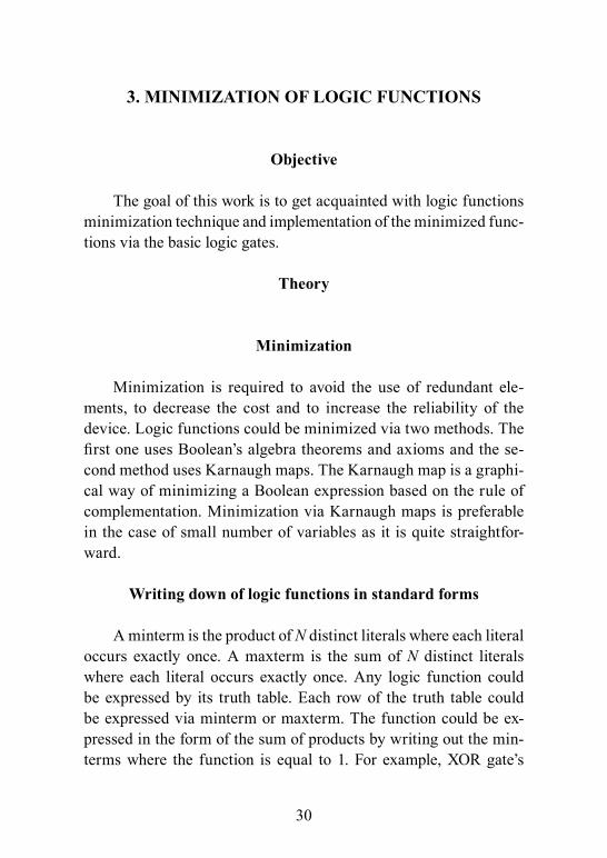
As an example let’s analyze the function presented in formu-la 3.3. This expression includes three variables, so the filled in the Karnaugh map (Fig. 3.1) will be made of 32 8= squares.
34
c2
( , , )F A B C
00
1
1
1
1
1
01 11 10
0
1
BC
A
c1
c2
Fig. 3.1 Karnaugh map of F(A,B,C)
every 1 of logic function is written into a related square, 1 cor-responding to minterm with number 0 is written into 000 square, the 2nd 1 is written into 010 square and so on. now, according to the rules, the square contours should be drawn to include all 1’s. in this case minimum number of contours possible is 2, c1 is made of four 1’s (011, 010, 111, 110) and c2 is connecting the opposite sides of the Karnaugh map and is made of two 1s (000, 010). Vertical side of c1 has different values for input A, and therefore A will not be written into minimized expression. horizontal side of c1 has two inputs B and C. At first input B is checked, and in all squares of the contour its value is 1 (011, 010, 111 and 010), so B should be written into the expression. input C has different values in the squares of contour c1 (011, 010, 111 and 010), so it will not be written into the expression. contour c2 has the same 0 value (000 and 010) for input A, so A should be written into minimized expression; for the horizontal side input B has different values (000 and 010), so it will not be written into the expression; input C has the same value 0 (000 and 010), so C should be written into the expression. The final minimized expression will be:
( , , ) 1 2F A B C c c B AC= + = + (3.5)
A different example made of function with 4 logic variables:
( )( , , , ) 2,3,6,7,8,9,12,13F W X Y Z m= ∑ (3.6)

35
The Karnaugh map filled with minterms is presented in Fig. 3.2:
( , , , )F W X Y Z
00
1
1
1
1
01 11 10YZ
WX
1
1
1
1
00
01
11
10
c2
c1
Fig. 3.2 Karnaugh map of F(W,X,Y,Z)
here two contours c1 and c2 will hold all the 1s and the mini-mized expression will be:
( , , , ) 1 2F W X Y Z c c WY WY= + = + (3.7)
A more complex example of the Karnaugh map made of 11 ones and 2 don’t care outputs (d) is presented in Fig. 3.3.
( , , , )F A B C D1
00
1
1
d
1 d
1
01 11 10CD
AB
1 1
1
1
1
1
00
01
11
10
c1
c1
c3
c2
Fig. 3.3 Karnaugh map of F(A,B,C,D)

36
to minimize this function four contours are made. Only one don’t care output (d) was included into contour c1 according to min-imization rule 2. The final minimized expression in the form of the sum of products is:
( , , , ) 1 2 3F W X Y Z c c c AD BD AB= + + = + + (3.8)
tasks
during the laboratory work you will receive different tasks from the tutor.
example of the obligatory tasks (for 6 points out of 10 pos-sible):
1. minimize logic function and design the circuit of the minimized function. check if the truth table is right.
( )( , , , ) 0,2,4,5,8,10,12,13F A B C D m= ∑ . (3 points)2. minimize logic function and design the circuit of the
minimized function. check if the truth table is right. ( , , , ) ( )F W X Y Z W X WXY WXY Z= + + . (3 points)
example of the additional task (4 points):3. Fill in the truth table of the function
( , , , )F A B C D A B C D= ⊕ ⊕ ⊕ and show it to the tutor. design a circuit and check if the truth table is the same.
Control questions
1. What do terms “minterm” and “maxterm” mean?2. Write function ( )( , , ) 2,3,6,7F X Y Z m= ∑ in the conjunc-
tive normal form (product of sums in expanded form).3. Write function ( )( , , ) 2,4,5,7F X Y Z M= ∏ in the disjunc-
tive normal form (sum of products in expanded form).
37
4. Write function ( )( , ) 2,3F X Y m= ∑ in the disjunctive nor-mal form.
5. how many 1s should be included into one contour?6. how many contours should be drawn in one Karnaugh map?7. draw the Karnaugh map for this function:
( )( , , ) 4,5,7F X Y Z m= ∑ . minimize the function.8. draw the Karnaugh map for this function:
( )( , , ) 0,2,6F X Y Z M= ∏ . minimize the function.9. draw the Karnaugh map for this function:
( , , )F A B C AB C B= + + . minimize the function.10. draw the Karnaugh map for this function:
( , , , ) ( )F A B C D A C D ACD ABCD= + ⋅ + + . minimize the function.
11. draw the Karnaugh map for this function: ( ) ( )( )( , , ) 4,5,7 6F X Y Z m x= +∑ . minimize the func-
tion.12. draw the Karnaugh map for this function:
( ) ( )( )( , , , ) 1,4,5,7 2,3,6F A B C D m x= +∑ . minimize the function.
13. draw the Karnaugh map for this function: ( , , )F A B C A B C= ⊕ ⊕ . is it possible to minimize this
function?
Literature
1. Kleitz, W. (2008). Digital Electronics: A Practical Ap-proach. mcGraw hill, p. 166–175.
2. lala, Parag, K. (2007). Principles of Modern Digital De-sign. A John Willey & sons inc., p. 60–73.
3. Kirvaitis, r. (2000). Digital Devices. E-Text-book. Avail-able from the author, p. 22–30.
4. Kirvaitis, r. (1999). Loginės schemos. Vilnius: enciklope-dija, p. 39–52. (in lithuanian)
38
4. aLGebRaiC minimiZation oF LoGiC FunCtions
objective
the goal of this work is to get acquainted with the basic theo-rems and axioms of Boolean algebra and to learn to apply them for minimization of logic functions.
theory
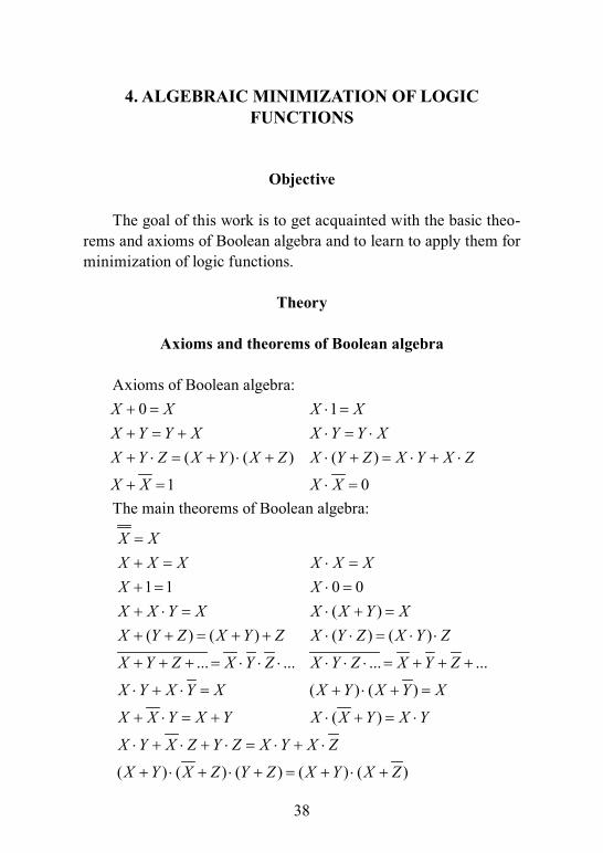
axioms and theorems of boolean algebra
Axioms of Boolean algebra:0 1
( ) ( ) ( )
1 0
X X X XX Y Y X X Y Y XX Y Z X Y X Z X Y Z X Y X Z
X X X X
+ = ⋅ =+ = + ⋅ = ⋅+ ⋅ = + ⋅ + ⋅ + = ⋅ + ⋅
+ = ⋅ =the main theorems of Boolean algebra:
1 1 0 0( )
( ) ( ) ( ) ( )
... ... ... ...
( ) ( )
( )
( ) ( ) ( ) ( ) ( )
X XX X X X X XX XX X Y X X X Y XX Y Z X Y Z X Y Z X Y Z
X Y Z X Y Z X Y Z X Y Z
X Y X Y X X Y X Y X
X X Y X Y X X Y X Y
X Y X Z Y Z X Y X Z
X Y X Z Y Z X Y X Z
=+ = ⋅ =+ = ⋅ =+ ⋅ = ⋅ + =+ + = + + ⋅ ⋅ = ⋅ ⋅
+ + + = ⋅ ⋅ ⋅ ⋅ ⋅ ⋅ = + + +
⋅ + ⋅ = + ⋅ + =
+ ⋅ = + ⋅ + = ⋅
⋅ + ⋅ + ⋅ = ⋅ + ⋅
+ ⋅ + ⋅ + = + ⋅ +

39
algebraic minimization
minimizing of expression algebraically involves application of axioms and theorems until the expression could not be further mini-mized. One way of algebraic minimization similar to Karnaugh map minimization is repeated application of the rule of complementation X Y X Y X⋅ + ⋅ = , starting with the function in disjunctive normal form by writing out minterms where the function is equal to 1, and ending up with the minimized expression made of a set of product terms called prime implicants.
common algebraic minimization rules:1. Write a function in a disjunctive normal form.2. Find terms which have the same variables and differ by
inversion of one variable only.3. combine these terms, removing that variable (application
of the rule of complementation).4. After combining all the terms that could be combined a
new expression could be written down.5. steps 2–4 are repeated until no more terms could be com-
bined.By following the minimization rules it is possible to minimize
the function to a form where no further minimization is possible. Also these minimization steps could be used for expressions with more variables (6 or more), when the simplest application of the Karnaugh map is not reasonable.
When it is not clear how to write the initial expression in dis-junctive normal form (not clear which axioms and theorems to ap-ply), the truth table of the function could be filled and from the truth table the expression in disjunctive normal form could be written.

40
methodology
As an example the logic function ( )( , , , ) 2,3,6,7,8,9,12,13F W X Y Z m= ∑ will be algebraically
minimized. the initial expression of the function in the disjunctive normal form (sum of products in expanded form by writing out the minterms where the function is equal to 1) is:
( )( , , , ) 2,3,6,7,8,9,12,13F W X Y Z m
W XY Z W XYZ W XY Z W XYZ
W X Y Z W X YZ WXY Z WXYZ
= =
= + + + +
+ + + +
∑ (4.1)
The first and the second terms differ by one inverted varia-ble Z only, so they could be combined by removing the variable Z: W XY Z W XYZ W XY Z+ = W XY Z+ W XY= , a similar situation is with another 3 pairs of terms. So after the first pass the expression will be F W XY W XY W X Y WXY= + + + . here again the first two terms differ by the inverted variable X, and other two differ by the inverted variable X. so after the second pass the new expression is F WY WY= + . this expression has no terms which could be combined so it is assumed that this is the final minimized expression of the original function.
tasks
during the laboratory work you will receive different tasks from the tutor.
example of the obligatory tasks (for 6 points out of 10 pos-sible):
1. minimize the function using algebraic minimization rules: ( )( , , , ) 1,3,4,6,9,11,12,14F A B C D m= ∑ . simulate the
minimized function and check if the truth table is the same. show the results to the tutor. (4 points)

41
2. minimize this function by applying Boolean algebra axioms and theorems: (( ) )F D A A B AB BD= + + + . (2 points)
example of the additional task (4 points):3. Perform the algebraic minimization of this function:
( , , , , ) (0,2,5,7,8,10,13,15,16,18,21,23,24,26,29)F A B C D E M= ∏
Control questions
1. What are the common minimization rules for Boolean al-gebraic minimization?
2. state the rule of complementation.3. Write this function in the expanded disjunctive normal
form: ( )( , , ) 1,3,4,6F A B C m= ∑ .4. Write this function in the expanded disjunctive normal
form: ( )( , , ) 0,1,2,3F A B C M= ∏ .5. minimize the function: ( , , , ) F A B C D AC D ACD AC= + + .6. minimize the function: ( )( , , ) 4,5,7F X Y Z m= ∑ .7. minimize the function: ( )( , , ) 0,1,2,3F A B C m= ∑ .8. minimize the function: ( )( , , , ) 0,1,2F A B C D M= ∏ .9. minimize the function: ( )( , , , ) 5,7,13,15F A B C D M= ∏ .10. minimize the function: ( )( , , )F A B C A BA B ABC= + ⋅ + .11. By applying axioms and theorems of Boolean algebra min-
imize this function: ( , , ) ( )( )F X Y Z X Y Y Z= + + .12. By applying axioms and theorems of Boolean algebra min-
imize this function: ( , , )F X Y Z X XY XZ= + + .13. By applying axioms and theorems of Boolean algebra min-
imize this function: ( , , ) ( )F X Y Z X Y Z X= ⋅ + + .

42
Literature
1. Kleitz, W. (2008). Digital Electronics: A Practical Ap-proach. mcGraw hill, p. 130–180.
2. lala, Parag, K. (2007). Principles of Modern Digital De-sign. A John Willey & sons inc., p. 73–79.
3. Kirvaitis, r. (2000). Digital Devices. E-Text-book. Avail-able from author, p. 22–30.
4. Kirvaitis, r. (1999). Loginės schemos. Vilnius: enciklope-dija, p. 39–52 (in lithuanian).

43
5. bJt sWitCH. inVestiGation oF RtL anD DtL Gates
objective
the goal of this work is to get acquainted with the bipolar junc-tion transistor switch and investigate the gates of resistor transistor logic and diode transistor logic.
theory
bJt switch
BJt switch is made of bipolar junction transistor (Fig. 5.1) and loading resistor. it operates as an inverter.
Fig. 5.1 investigation circuit of BJt switch
44
BJt is controlled by the base current. When the saturating cur-rent flows through the base of the transistor (logic one supplied), transistor is saturated and the output is connected to the ground through the collector-emitter circuit (logic zero). When the current is not flowing through the base (logic zero applied), transistor is closed and its resistance is very high, so the power supply voltage (logic one) is present at the output.
RtL
resistor transistor logic (rtl) is a simple circuit made of re-sistors connected to BJt switch usually implementing nOr logic function. input circuit of rtl nOr gate is shown in Fig. 5.2.
Fig. 5.2 input circuit of rtl gate

45
DtL
diode transistor logic (dtl) is a circuit similar to rtl, but in-stead of resistors diodes are used. this circuit is suitable for nOr gate implementation. input circuit of dtl nOr gate is shown in Fig. 5.3.
methodology
For modeling of BJt switch the virtual n-p-n transistor is ne-cessary. Voltmeters are used to determine the logic level at the input and output. interconnection scheme is presented in Fig. 5.1.
When the switch is turned off (base of transistor is shorted to the ground) no current flows through the closed base-emitter junc-tion. transistor is closed and the resistance of the closed transistor is very high. So there is almost no current flow through the transistor. in this case almost all power supply voltage drops on the transistor and logic value in output is high. When the switch is turned on, the current through the base-emitter junction will saturate the transistor and voltage drop on the saturated transistor will be low (0.1-0.2 V).
Fig. 5.3 input circuit of dtl gate

46
calculation of voltages in input circuit of rtl gate is based on Ohm’s law. For each possible combination of voltages at inputs the output voltage should be calculated and written into the truth table. in our case (Fig. 5.2) voltages for logic zero and logic one at inputs are 0 0 VU = and 1 5 VU = . With such inputs denoted as A, B and C the left part of the truth table can be filled (Table 5.1).
As an example for the inputs combination as presented in Fig. 5.2, calculation will be as follows. The first input is connected to 5 V and all other inputs are connected to the ground 0 V. in our case R1 is connected in series with parallel connection of R2, R3 and R4. the total resistance RΣ of parallel connected resistors should be evaluated first. Next the current could be calculated and then the voltage drop at the output. All the necessary calculations are pre-sented below (5.1). this way the calculation should be performed for each combination of inputs in the truth table (table 5.1).
1 0
2|| 3|| 4
1 2 || 3 || 4,1 1 12 || 3 || 4 k ,1 1 1 1 1 1 3
2 3 41 41 k ,3 3
(5 0) 3 15 mA,4 4
15 12 || 3 || 4 1.25 V.4 3R R R
R R R R R
R R R
R R R
R
U UIR
U I R R R
∑
∑
Σ
= +
= = = Ω+ ++ +
= + = Ω
− − ⋅= = =
= ⋅ = ⋅ =
(5.1)

47
table 5.1 truth table in volts of input circuit of rtl gate
A B C F
0 0 0 00 0 5 1.250 5 0 1.250 5 5 2.55 0 0 1.255 0 5 2.55 5 0 2.55 5 5 3.75
in the case of dtl gate, diodes are used instead of input resistors R1, R2 and R3 (Fig. 5.3). With diodes, calculation is much simpler, as the only thing that matters is the voltage drop on diode dU . As the voltage drop is the same for all diodes, assuming they are of the same type, parallel connection of diodes will still give the same forward voltage drop dU (for the silicon diode d 0.7 VU = ). When all diodes are connected to the ground the output voltage will be zero, and when at least one input is connected to the power supply, the output voltage will be: 1 0
d 5 0 0.7 4.3 VU U U U= − − = − − = . (table 5.2)
table 5.2 truth table in volts of input circuit of dtl gate
A B C F0 0 0 00 0 5 4.30 5 0 4.30 5 5 4.35 0 0 4.35 0 5 4.35 5 0 4.35 5 5 4.3

48
tasks
during the laboratory work you will receive different tasks from the tutor.
example of the obligatory tasks (for 6 points out of 10 pos-sible):
1. design BJt switch. connect all the required tools (power supply, voltmeters) and check if the switch is working as an inverter. (2 points)
2. calculate the output voltages of input circuit of rtl gate for all possible values of voltages in inputs (let 0 0 VU = and 1 4 VU = ) and fill in the truth table in volts. The resis-tances of resistors are: R1 = R2 = R3 = R4 = 1 kΩ. Simu-late the circuit and compare the measured values with the calculated ones. (2 points)
Fig. 5.4 input circuit of rtl gate
3. replace resistors R1, R2, R3 in Fig. 5.4 with diodes, calcu-late the output voltages and fill in the truth table in volts. next simulate the circuit and compare the measured values with the calculated ones. (2 points)

49
example of the additional task (4 points):4. the circuit (Fig. 5.5) is made of rtl gates, each with one
transistor. When the input is high the total circuit current consumption from the power supply is 12 mA, when the input is low the total circuit current consumption is 9 mA. calculate the current consumption of one gate:
a. When its input is high.b. When its input is low.
1≥ 1≥ 1≥
Fig. 5.5 logic gates connected in series
Control questions
1. explain the operation of BJt switch.2. state Ohm’s law.3. What will be the forward voltage drop on silicon diode?4. What will be the forward voltage drop on two silicon di-
odes connected in parallel?5. What will be the forward voltage drop on two silicon di-
odes connected in series?6. explain the calculation procedure of input circuit of rtl
gate.7. explain the calculation procedure of input circuit of dtl
gate.

50
Literature
1. Kleitz, W. (2008). Digital Electronics: A Practical Ap-proach. mcGraw hill, p. 39–47.
2. Kirvaitis, r. (2000). Digital Devices. E-Text-book. Avail-able from author, p. 31–36.
3. Kirvaitis, r. (1999). Loginės schemos. Vilnius: enciklope-dija, p. 54–66. (in lithuanian)

51
6. inVestiGation oF stanDaRD ttL Gate
objective
the goal of this work is to get acquainted with operation of standard ttl gate, calculate and measure parameters of the gate.
theory
Before analyzing ttl gate it is necessary to analyze voltage drops across saturated bipolar n-p-n transistor (Fig. 6.1).
0.2V
0.7V
0.5V
e
c
B+
_
++
_
_
Fig. 6.1 saturated bipolar n-p-n transistor
the circuit of standard ttl gate is presented in Fig. 6.2 (usu-ally it has 2 or more inputs, however here all the inputs are presented as one input a). to understand how ttl gate works it is necessary to analyze voltages at key points denoted by letters (a, d, e, f, g, h, k) and fill the table of voltages at these points.
calculation is started from the low voltage of 0.2V supplied at input a. low emitter voltage and high base voltage will cause transistor Vt1 to saturate. Voltage drop on the saturated transis-tor’s base-emitter junction is 0.7 V and moving from the emitter to the base will cause voltage rise. so at point d voltage will be 0.2 + 0.7 = 0.9 V. By moving from the base to the collector voltage drop is 0.5 V so at point e voltage will be 0.9 – 0.5 = 0.4 V. such

52
voltage is not enough to open two base-emitter junctions of Vt2 and Vt4 transistors, so Vt2 transistor’s base-emitter junction resis-tance will be very high, much higher than R2 or R3, so almost all power supply voltage will drop on the closed transistor Vt2 and at point h voltage will be +e and at point g voltage will be al-most zero what will cause the transistor Vt4 to be closed. Because of the high potential at point h, transistor Vt3 will be saturated and voltage drop across its base-emitter junction will be 0.7 V. so at point k voltage will be E – 0.7 V and at point f voltage will be E – 0.7 – 0.7 V = E – 1.4 V because of the additional voltage drop 0.7 V on diode Vd. the usual power supply voltage for the ttl gate is 5 V, so the high level in ttl output will be 5 – 1.4 = 3.6 V.
Fig. 6.2 ttl gate

53
When the high level 3.6 V is supplied at input a the circuit be-haves in a different way. now input transistor Vt1 is working in the reverse mode and its base-emitter junction is closed. that will cause a high potential at point d that will open the base-collector junction of Vt1 and the base-emitter junctions of Vt2 and Vt4. now voltage at point g will be equal to voltage drop on the saturated base-emitter junction of Vt4 that is 0.7 V. A similar situation is true for point e, here additional 0.7 V will be added on the base-emitter junction of Vt2 transistor, so the total voltage at point e will be 0.7 + 0.7 = 1.4 V. the saturated base-collector junction of Vt1 work-ing in reverse mode will give an additional 0.7 V voltage drop so at point d voltage will be 1.4 + 0.7 = 2.1 V. As Vt2 is open, voltage at point h will be 1.4 – 0.5 = 0.9 V because of voltage drop of 0.5 V on the base-collector junction of Vt2. the potential at point h could also be calculated from point g and voltage drop on the saturated Vt2: 0.7 + 0.2 = 0.9 V. At point f voltage drop on the saturated Vt4 will be 0.2 V. the last point is k, here voltage potential between h and f is divided between the two closed p-n junctions: the first – base-emitter junction of Vt3 and the second – junction of diode Vd: (0.9 – 0.2)/2 = 0.35 V per junction. so voltage at point k will be 0.2 + 0.35 = 0.55 V. All voltages are presented in table 6.1.
table 6.1 Voltages in key points of ttl gate
Point u, V u, Va 0.2 3.6d 0.9 2.1e 0.4 1.4f e – 1.4 0.2g 0 0.7h e 0.9k e – 0.7 0.55

54
When input a is high, Vt1 transistor is working in the reverse mode. The reverse current gain coefficient βrev is very small com-pared to the forward current gain coefficient β. in case of the reverse mode, the current flows from emitter and base to collector. Knowing, that the bipolar junction transistor amplifies current, the collector current, when transistor is in reverse mode, could be expressed via the base current and βrev coefficient: c B e B rev Bi i i i ib= + = + βreviB. The fi-nal expression for the reverse current gain coefficient is βrev rev e B/i ib = . so to calculate βrev it is necessary to measure emitter and base cur-rents when the transistor is working in the reverse mode.
methodology
to analyze operation of ttl gate, it should be simulated using virtual components. Of course, parameters of virtual components may be different than those of the real devices. nevertheless the model still provides enough precision and virtual parameters could be changed to approximate physical device. to measure voltages at key points (Fig. 6.2) it is necessary to connect voltmeters between key points and the ground. to measure the current it is necessary to use ammeters connected in series with the branch where the current is measured in.
connection of the sources of input voltages and ammeters to VT1 transistor for calculation of the reverse current gain coefficient is shown in Fig. 6.3.

55
Fig. 6.3 connection of ammeters and sources of input voltages
the tasks
during the laboratory work you will receive different tasks from the tutor.
example of the obligatory task (for 6 points out of 10 possible):1. simulate the standard ttl gate with one input. connect
4 kΩ resistor into VT1 base, 1.6 kΩ resistor into VT2 col-lector and 1 kΩ resistor into VT2 emitter. Connect 130 Ω protecting resistor into Vt3 collector. next connect power supplies, voltmeters and ammeters to the circuit.calculate voltages at key points (a, d, e, f, g, h, k) and write them into the table for high (3.6 V) and low (0.2 V) input levels. next measure voltages at the same points for high and low input signals and also write them into the table. show the table with voltage values at key points to the tutor and answer the tutor’s questions.

56
example of the additional tasks (2 points each):2. Perform the necessary measurements and calculate the re-
verse current gain coefficient of VT1.3. Perform the necessary measurements to calculate the pyra-
miding factor (the maximum number of ttl gates that could be connected to the output of ttl gate under inves-tigation without change in the logic level).
Control questions
1. draw the symbols of n-p-n and p-n-p transistors and show their bases, collectors and emitters.
2. Write the voltage drops between the electrodes of saturated n-p-n transistor – absolute values and polarities.
3. What does the forward current gain coefficient b mean?4. explain the operation of ttl gate when input signal is low
(0.2 V).5. explain the operation of ttl gate when the input signal is
high (3.6 V).6. What the diode Vd is used for in ttl gate?7. design the standard ttl gate and check what the mini-
mum possible voltage of input signal is needed to obtain the low level at the output of the gate. how this information could be used to calculate the pyramiding factor (the maxi-mum number of ttl gates that could be connected to the output of the current ttl gate)?
8. in what mode will Vt1 operate when the high level (3.6 V) is applied at input a?
9. What currents should be measured to calculate the reverse current gain coefficient βrev?

57
Literature
1. Kleitz, W. (2008). Digital Electronics: A Practical Ap-proach. mcGraw hill, p. 46–50, 56–57, 326–346.
2. Kirvaitis, r. (2000). Digital Devices. E-Text-book. Avail-able from the author, p. 36–39.
3. Kirvaitis, r. (1999). Loginės schemos. Vilnius: enciklope-dija, p. 67–71. (in lithuanian)

58
7. inVestiGation oF mos anD Cmos sWitCHes
objective
the goal of this work is to get acquainted with mOs and cmOs switch, cmOs logic gates and measuring of cmOs parameters.
theory
MOSFET is a metal-oxide-semiconductor field-effect transistor. Field-effect transistors (Fet) are unipolar devices, where the current through the channel is carried by the flow of only one type of carriers: either electrons in n-type channel or holes in p-type channel. cross-sections of two types of mOsFet transistors with induced channels that will be used in this work are presented in Fig. 7.1. the current through the induced channel of mOsFet is controlled by applying voltage to the insulated from substrate gate (G) and inducing a con-ducting channel. the minimum gate voltage required to induce the channel is called the threshold voltage and it is different for various types of mOsFets. resistance of a channel of the saturated transistor is low, what makes small heat dissipation in transistors of mOs logic. in the case of n-channel enhanced mOsFet (Fig. 7.1 a) the positive voltage applied to the gate is attracting electrons to form a conducting channel and the potential difference between source (s) and drain (d) will cause the current in the channel. the junction between n-channel and p-substrate must be reverse biased – it happens when p-substrate is connected to the most negative potential, i.e., when it is grounded.
in the case of p-channel enhanced mOsFet (Fig. 7.1 c) the negative voltage applied to the gate repels the electrons (attracts holes) to form a conducting p-channel. the n-substrate should be connected to the most positive terminal, i.e., power supply.

59
mass produced mOsFets usually have their substrates con-nected with one of their terminals (source), so the care should be taken interconnecting transistors to avoid short circuit.
a)
p
n+ n+
source drainGate
substrateb)
s
d
Gsubstrate
c)
n
p+ p+
source drainGate
substrated)
s
d
Gsubstrate
Fig. 7.1 mOsFets with induced channels a) n-type c) p-type and their graphical representations b) n-type d) p-type
simple switch made of n-channel enhancement mOsFet is shown in Fig. 7.2. the circuit is actually made of two parts: the upper part with transistor Vt1 and the lower part with three transistors connected in parallel. since all the transistors are of the same kind, their drain-source resistance is also the same, so to achieve low output, when the input is high, the lower part should have drain-source resistance much lower (usually 10 times) than the upper part (VT1), but for the simplification of the circuit only three transistors in parallel are shown. in mass pro-duced devices the drain-source resistance of the Vt1 is designed ten times higher by changing either length or length and width of the gate so no parallel connection of transistors is needed.

60
cmOs switch (Fig. 7.3) is made of two different types of mOs-Fets with enhanced n and p-channels. high level input opens transis-tor Vt2 and closes transistor Vt1. When the input changes from high level to low, Vt1 starts opening and Vt2 starts closing. during the switching only there will be a short moment when both transistors are not fully closed and the current will flow. In this case the circuit has a very low power consumption compared to the previous simple mOs switch, as the current flows only, when the circuit state is changing. Because of the power efficiency standard CMOS is preferable in low power devices. however this circuit is not suitable for high frequency applications because the transconductance of Fet is not high enough to quickly charge or discharge the load capacitance. the exception is high speed cmOs in which capacitances are charged and discharged with current of short connected power source.
Fig. 7.2 mOs switch
cmOs technology is popular in the integrated circuits. to create a working logic gate performing nAnd or nOr function, one pair of transistors is necessary for each input. let’s analyze operation of 2nAnd gate (Fig. 7.4). this gate should generate a low output only

61
when all inputs are high. this condition could be true only when two transistors Vt2A and Vt2B connected in series are open, so they both short the output to the ground, and both Vt1A and Vt1B tran-sistors are closed. Any other combination of the input signals will cause at least one of Vt2 transistors to be closed and at least one of Vt1 transistors to be open, what will generate high output.
Fig. 7.3 cmOs switch
Fig. 7.4 cmOs 2nAnd gate
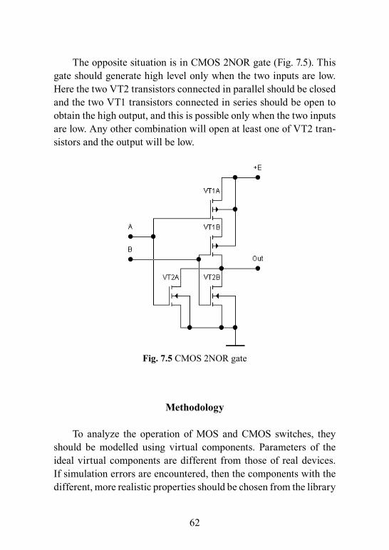
62
the opposite situation is in cmOs 2nOr gate (Fig. 7.5). this gate should generate high level only when the two inputs are low. here the two Vt2 transistors connected in parallel should be closed and the two Vt1 transistors connected in series should be open to obtain the high output, and this is possible only when the two inputs are low. Any other combination will open at least one of Vt2 tran-sistors and the output will be low.
Fig. 7.5 cmOs 2nOr gate
methodology
to analyze the operation of mOs and cmOs switches, they should be modelled using virtual components. Parameters of the ideal virtual components are different from those of real devices. if simulation errors are encountered, then the components with the different, more realistic properties should be chosen from the library

63
to approximate physical device. to measure voltages of inputs and outputs it is necessary to connect voltmeters. Voltages should be measured relative to the ground. to measure the current consumed by the circuit it is necessary to use ammeters connected in series with power supply. if the current is alternating, then the ammeter should be switched into Ac current measuring mode.
to analyze cmOs operation when different frequency input signal is applied, Function Generator tool from instruments panel is used. typical connection of the function generator is shown in Fig. 7.6. it is important to connect “common” pin to the ground and “+” pin to the input of the circuit. Amplitude and offset should be the same to keep the input signal on the positive side. Pulses should be of the square form to imitate the digital signals.
Fig. 7.6 Function generator connection
tasks
during the laboratory work you will receive different tasks from the tutor.
example of the obligatory tasks (for 6 points out of 10 possible):1. design mOsFet switch. connect power supplies,
switch and voltmeters and check operation of the circuit. (2 points)

64
2. design cmOs switch. connect power supplies and voltme-ters to switch and check operation of the circuit. (2 points)
3. design a cmOs 3nOr logic gate. connect power supplies, switches, voltmeters and check the operation of the circuit. Answer the tutor’s questions. (2 points)
examples of the additional tasks (2 points each):4. investigate how power supply current depends on frequen-
cy of switching of cmOs switch. design cmOs switch, connect ammeter in series with power supply, switch am-meter to Ac mode, connect function generator to the in-put of cmOs switch, set the amplitude to 2.5 V, offset to 2.5 V and the form of a signal to square. Perform current measurements when the input frequency is 1 khz, 10 khz, 100 khz and 1 mhz. draw the current dependence on fre-quency and show the results to the tutor.
5. use the same cmOs switch circuit as in task 4, but leave the frequency at 1 khz and check the current consumption when power supply voltage is 7 V, 5 V and 4 V. Write the results into the table and show them to the tutor.
Control questions
1. explain operation of the n-channel enhanced mOsFet.2. explain operation of mOs switch.3. explain operation of cmOs switch.4. Why standard CMOS technology is very power efficient on
the low frequencies and less efficient on high frequencies?5. how many transistors are necessary to design cmOs
4nAnd gate?6. design cmOs 3nAnd and 3nOr logic gates, then simu-
late them to check their operation.

65
Literature
1. Kleitz, W. (2008). Digital Electronics: A Practical Ap-proach. mcGraw hill, p. 346–351, 355–357.
2. Kirvaitis, r. (2000). Digital Devices. E-Text-book. Avail-able from the author, p. 42–47.
3. Kirvaitis, r. (1999). Loginės schemos. Vilnius: enciklope-dija, p. 82–94. (in lithuanian)
66
8. inVestiGation oF biCmos sWitCH
objective
the goal of this work is to get acquainted with the structure, operation and properties of BicmOs switch and BicmOs logic gates.
theory
cmOs technology proved to be power effective when the static power dissipation is in question. in the static mode power consump-tion is practically zero. High input impedance is another benefit of cmOs technology. however there is one major disadvantage – standard cmOs can’t work in a high frequency region with higher capacitive load. if Fet transistor’s channel is wide and its resistan-ce is small, it can conduct high currents and quickly discharge or charge the load capacitance; however with the increasing frequency of operation, the size of the circuit is decreased and so is the size of the transistor. An important feature of Fet and BJt is transcon-ductance: m /g I E= ∆ ∆ . transconductance points how the current through collector or drain I∆ changes with voltage change E∆ in the base or gate. As the size of Fet is reduced, the dimensions of the channel are reduced too. if the drain voltage is kept the same, the electric field increases along the channel, the carrier velocity saturates, and the limitation of the current and transconductance ap-pears. in this case the situation with BJt is better as the mobility of the carriers in BJt is higher, so the transconductance is higher. this way BJt can drive higher currents to charge and discharge the load capacitance and the frequency of operation is higher.
To use the benefits of both technologies the hybrid technology called BicmOs was created having the input stage made of cmOs

67
and the output stage made of BJt. simple BicmOs switch is pre-sented in Fig. 8.1.
59
Fig. 8.1 initial BicmOs switch
As the high voltage is applied to the input of the BicmOs switch, Vt1 p-channel enhanced mOsFet is closing. Because of the closed Vt1, Vt3 base-emitter junction is also closed. the same high voltage applied to the Vt2 n-channel enhanced mOsFet gate opens the transistor and if there any potential difference between the output and the ground, the potential through the base-emitter junction of Vt4 will open the Vt4 and any load capacitance will be discharged through the saturated Vt4 and its base-emitter junction. the dis-charge current will be: Be Vt4( 1)Iβ + .
When the low voltage is applied to the input, the Vt2 nmOsFet is closing together with Vt4. under low voltage the Vt1 pmOsFet is opening and the potential difference between the cir-cuit output and power supply voltage will cause the Vt3 transistor to open and charge the load capacitance through the collector-emitter circuit and base-emitter junction. the charge current will be:
Be Vt3( 1)Iβ + . One disadvantage of such circuit is that the maximum output
voltage will be lower than the power supply voltage by 0.7 V base-emitter junction potential of Vt3 and the low voltage will be about 0.7 V higher than the ground because of base-emitter potential of
Fig. 8.1 initial BicmOs switch
As the high voltage is applied to the input of the BicmOs switch, Vt1 p-channel enhanced mOsFet is closing. Because of the closed Vt1, Vt3 base-emitter junction is also closed. the same high voltage applied to Vt2 n-channel enhanced mOsFet gate opens the transistor and if there is any potential difference between the output and the ground, the potential through the base-emitter junction of Vt4 will open Vt4 and any load capacitance will be discharged through the saturated Vt4 and its base-emitter junction. the discharge current will be:
59
Fig. 8.1 initial BicmOs switch
As the high voltage is applied to the input of the BicmOs switch, Vt1 p-channel enhanced mOsFet is closing. Because of the closed Vt1, Vt3 base-emitter junction is also closed. the same high voltage applied to the Vt2 n-channel enhanced mOsFet gate opens the transistor and if there any potential difference between the output and the ground, the potential through the base-emitter junction of Vt4 will open the Vt4 and any load capacitance will be discharged through the saturated Vt4 and its base-emitter junction. the dis-charge current will be: Be Vt4( 1)Iβ + .
When the low voltage is applied to the input, the Vt2 nmOsFet is closing together with Vt4. under low voltage the Vt1 pmOsFet is opening and the potential difference between the cir-cuit output and power supply voltage will cause the Vt3 transistor to open and charge the load capacitance through the collector-emitter circuit and base-emitter junction. the charge current will be:
Be Vt3( 1)Iβ + . One disadvantage of such circuit is that the maximum output
voltage will be lower than the power supply voltage by 0.7 V base-emitter junction potential of Vt3 and the low voltage will be about 0.7 V higher than the ground because of base-emitter potential of
.When the low voltage is applied to the input, Vt2 nmOsFet
is closing together with Vt4. under low voltage Vt1 pmOsFet is opening and the potential difference between circuit output and power supply voltage will cause Vt3 transistor to open and charge the load capacitance through the collector-emitter circuit and base-emitter junction. the charge current will be:
59
Fig. 8.1 initial BicmOs switch
As the high voltage is applied to the input of the BicmOs switch, Vt1 p-channel enhanced mOsFet is closing. Because of the closed Vt1, Vt3 base-emitter junction is also closed. the same high voltage applied to the Vt2 n-channel enhanced mOsFet gate opens the transistor and if there any potential difference between the output and the ground, the potential through the base-emitter junction of Vt4 will open the Vt4 and any load capacitance will be discharged through the saturated Vt4 and its base-emitter junction. the dis-charge current will be: Be Vt4( 1)Iβ + .
When the low voltage is applied to the input, the Vt2 nmOsFet is closing together with Vt4. under low voltage the Vt1 pmOsFet is opening and the potential difference between the cir-cuit output and power supply voltage will cause the Vt3 transistor to open and charge the load capacitance through the collector-emitter circuit and base-emitter junction. the charge current will be:
Be Vt3( 1)Iβ + . One disadvantage of such circuit is that the maximum output
voltage will be lower than the power supply voltage by 0.7 V base-emitter junction potential of Vt3 and the low voltage will be about 0.7 V higher than the ground because of base-emitter potential of
.One disadvantage of such circuit is that maximum output vol-
tage will be lower than the power supply voltage by 0.7 V base-emitter junction potential of Vt3 and the low voltage will be about
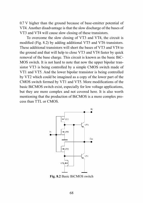
68
0.7 V higher than the ground because of base-emitter potential of Vt4. Another disadvantage is that the slow discharge of the bases of Vt3 and Vt4 will cause slow closing of these transistors.
to overcome the slow closing of Vt3 and Vt4, the circuit is modified (Fig. 8.2) by adding additional VT5 and VT6 transistors. these additional transistors will short the bases of Vt3 and Vt4 to the ground and that will help to close Vt3 and Vt4 faster by quick removal of the base charge. this circuit is known as the basic Bic-mOs switch. it is not hard to note that now the upper bipolar tran-sistor Vt3 is being controlled by a simple cmOs switch made of Vt1 and Vt5. And the lower bipolar transistor is being controlled by Vt2 which could be imagined as a copy of the lower part of the CMOS switch formed by VT1 and VT5. More modifications of the basic BicmOs switch exist, especially for low voltage applications, but they are more complex and not covered here. it is also worth mentioning that the production of BicmOs is a more complex pro-cess than ttl or cmOs.
60
Vt4. Another disadvantage is that the slow discharge of the bases of Vt3 and Vt4 will cause the slow closing of these transistors.
to overcome the slow closing of Vt3 and Vt4, the circuit is modified (Fig. 8.2) by adding additional Vt5 and Vt6 transistors. these additional transistors will short the bases of the Vt3 and Vt4 to the ground and that will help to close Vt3 and Vt4 faster by quick removal of the base charge. this circuit is known as the basic BicmOs switch. it is not hard to note that now the upper bipolar transistor Vt3 is being controlled by a simple cmOs switch made of Vt1 and Vt5. And the lower bipolar transistor is being controlled by Vt2 which could be imagined as a copy of the lower part of the cmOs switch formed by Vt1 and Vt5. there exist more modifica-tions of the basic BicmOs switch especially for low voltage applica-tions, but they are more complex and not covered here. it is also worth mentioning that the production of BicmOs is a more complex process than ttl or cmOs.
Fig. 8.2 Basic BicmOs switch Fig. 8.2 Basic BicmOs switch

69
With the basic BicmOs switch nAnd and nOr logic gates could be designed. the design is very similar to cmOs nAnd and nOr gates. With the only difference that output BJt stage and BJt base discharge circuits are present. the rule is that for every ad-ditional input another three mOsFets should be added to the basic BicmOs switch.
61
With the basic BicmOs switch nAnd and nOr logic gates could be designed. the design is very similar to cmOs nAnd and nOr gates. With only difference that the output BJt stage and BJt base discharge circuits are present. the rule is that for every addi-tional input another three mOsFets should be added to the basic BicmOs switch.
Fig. 8.3 BicmOs 2nAnd gate
let’s analyze 2nAnd gate (Fig. 8.3) in detail. the upper input stage made of Vt1A, Vt1B, Vt5A and Vt5B is a cmOs 2nAnd gate which is controlling Vt3 output transistor. the lower input stage made of Vt2A and Vt2B is actually a copy of the Vt5A and Vt5B (lower part of cmOs 2nAnd gate) and it is used to control
Fig. 8.3 BicmOs 2nAnd gate
let’s analyze 2nAnd gate (Fig. 8.3) in detail. the upper input stage made of Vt1A, Vt1B, Vt5A and Vt5B is a cmOs 2nAnd gate which is controlling Vt3 output transistor. the lower input stage made of Vt2A and Vt2B is actually a copy of Vt5A and Vt5B (lower part of cmOs 2nAnd gate) and it is used to control

70
Vt4 output transistor. Vt6 remains the same. if at least one input A or B is low, then at least one Vt5A or Vt5B will be closed and at least one Vt1A or Vt1B will be open. that will cause a Vt3 to open. in the lower part of the circuit at least one Vt2A or Vt2B will be closed and Vt6 will be open that will cause Vt4 to be closed. if both inputs A and B are high, then Vt1A and Vt1B are closed, Vt5A and Vt5B are open, forcing Vt3 to close. in the lower part of the circuit both Vt2A and Vt2B are open and Vt6 is closed, so Vt4 will be open to discharge the load capacitance.
62
the Vt4 output transistor. Vt6 remains the same. if at least one input A or B is low, then at least one Vt5A or Vt5B will be closed and at least one Vt1A or Vt1B will be open. that will cause a Vt3 to open. in the lower part of the circuit at least one Vt2A or Vt2B will be closed and Vt6 will be open that will cause the Vt4 to be closed. if both inputs A and B are high, then Vt1A and Vt1B are closed, Vt5A and Vt5B are open, forcing the Vt3 to close. in the lower part of the circuit both Vt2A and Vt2B are open and Vt6 is closed, so Vt4 will be open to discharge the load capacitance.
Fig. 8.4 BicmOs 2nOr gate
BicmOs 2nOr gate is presented in Fig. 8.4. the gate consists of 2nOr cmOs circuit made of Vt1A, Vt1B, Vt5A and Vt5B as an upper input stage and a copy of lower part of 2nOr cmOs gate
Fig. 8.4 BicmOs 2nOr gate
BicmOs 2nOr gate is presented in Fig. 8.4. the gate consists of 2nOr cmOs circuit made of Vt1A, Vt1B, Vt5A and Vt5B

71
as an upper input stage and a copy of lower part of 2nOr cmOs gate (Vt2A, Vt2B) as a lower input stage of BicmOs 2nOr gate. Placement of Vt3, Vt4 and Vt6 is the same as in the case of the basic BicmOs switch.
if at least one input A or B is high, then at least one Vt1A or Vt1B transistor will be closed and at least one Vt5A or Vt5B will be open shorting base of Vt3 to the ground and closing it. Also Vt6 will be closed, too. At the same time at least one Vt2A or Vt2B will be open allowing the potential difference between the output and the ground to open Vt4 transistor. When both inputs A and B are low, both Vt1A and Vt1B transistors are open, and both Vt5A and Vt5B are closed, high potential difference will open Vt3 and Vt6 transistors. Vt2A and Vt2B will be closed and Vt6 will short the base of Vt4 to the ground, closing it.
methodology
to analyze the operation of BicmOs gates, they should be mod-elled using virtual components. to avoid simulation errors it is recom-mended to model one circuit at a time and if the simulation software cannot converge to solution, replace one component with the realistic model and again check the circuit operation. to measure voltages in inputs and outputs it is necessary to connect voltmeters to inputs and outputs. Voltages should be measured relative to the ground.
to analyze BicmOs operation with different capacitive load, the capacitor should be connected to the output of BicmOs switch and a constant frequency input signal should be applied through Function Generator tool from “instruments” panel. typical connec-tion of function generator is shown in Fig. 8.5. it is important to connect “common” terminal to the ground and “+” terminal to the input of the circuit. Amplitude and offset should be the same to keep the input signal on the positive side. Pulses should be of the square form to imitate the digital signals.
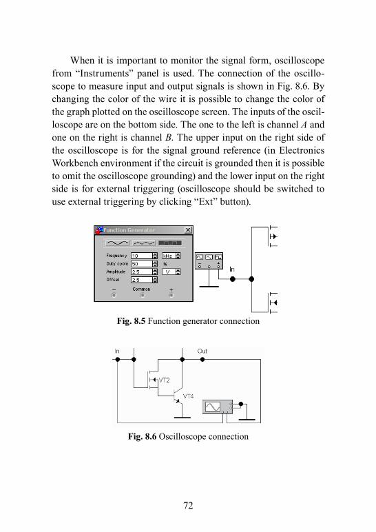
72
When it is important to monitor the signal form, oscilloscope from “instruments” panel is used. the connection of the oscillo-scope to measure input and output signals is shown in Fig. 8.6. By changing the color of the wire it is possible to change the color of the graph plotted on the oscilloscope screen. the inputs of the oscil-loscope are on the bottom side. the one to the left is channel A and one on the right is channel B. the upper input on the right side of the oscilloscope is for the signal ground reference (in electronics Workbench environment if the circuit is grounded then it is possible to omit the oscilloscope grounding) and the lower input on the right side is for external triggering (oscilloscope should be switched to use external triggering by clicking “ext” button).
64
When it is important to monitor the signal form, an Oscilloscope from the “instruments” panel is used. the connection of the oscillo-scope to measure the input and output signals is shown in Fig. 8.6. By changing the color of the wire it is possible to change the color of the graph plotted on the oscilloscope screen. the inputs of the oscil-loscope are on the bottom side. the one to the left is channel A and one on the right is channel B. upper input on the right side of the oscilloscope is for the signal ground reference (in electronics Work-bench environment if the circuit is grounded then it is possible to omit the oscilloscope grounding) and the lower input on the right side is for external triggering (oscilloscope should be switched to use external triggering by clicking the “ext” button).
Fig. 8.5 Function generator connection
Fig. 8.6 Oscilloscope connection
Fig. 8.5 Function generator connection
Fig. 8.6 Oscilloscope connection

73
tasks
during the laboratory work you will receive different tasks from the tutor.
example of the obligatory tasks (for 6 points out of 10 pos-sible):
1. design the most simple BicmOs switch. connect power supplies, voltmeters and check operation of the circuit. show the working circuit to the tutor. (2 points)
2. design the basic BicmOs switch and cmOs switch. con-nect power supplies, switches, voltmeters and check opera-tion of the circuits. compare output voltages of both cir-cuits when high and low input signals are applied. show the circuits to the tutor and explain the differences. (4 points)
example of the additional task (4 points):4. design BicmOs 2nOr logic gate. connect power sup-
plies, switches, voltmeters. check operation of the circuit and answer the tutor’s questions.
Control questions
1. What are the main advantages of cmOs technology?2. What is the main disadvantage of the standard cmOs tech-
nology?3. What does term “transconductance” mean? compare the
transconductances of Fet and BJt.4. What are the differences between ttl technology and the
standard cmOs?5. What are the differences between BicmOs technology and
the standard cmOs?6. explain operation of the basic BicmOs switch.

74
7. What Vt6 transistor is used for in the basic BicmOs switch?
8. how many transistors (mOsFets and BJt) are necessary to design a BicmOs 3nAnd gate?
9. design BicmOs 3nAnd and 3nOr logic gates, then im-plement them and check their operation.
Literature
rabaey, J. m. (1996). Digital Integrated Circuits: A Design Perspective. Prentice hall. 1996 (Addendum B. the Bic-mOs Approach, p. 1–19.)

75
9. DesiGn oF aRitHmetiC DeViCes
objective
the goal of this work is to manage design of simple gate level arithmetic devices.
theory
let’s analyze a few simple arithmetic devices: half-adder, full adder and subtractor.
the simplest one is a half-adder (Fig. 9.1). it is designed to add the two least significant bits at the input and provide the binary sum at the output via the S and carry out outC . the truth table of half-adder is presented in table 9.1. From this table direct logic expres-sions for each of the outputs of the half-adder could be written. For the sum output: S AB AB A B= + = ⊕ and for the carry output:
outC AB= .
table 9.1 truth table of half-adder
A B Cout S0 0 0 00 1 0 11 0 0 11 1 1 0
67
9. DesiGn oF aRitHmetiC DeViCes
objective
the goal of this work is to manage design of simple gate level arithmetic devices.
theory
let’s analyze a few simple arithmetic devices: half-adder, full adder and subtractor.
the simplest one is a half-adder (Fig. 9.1). it is designed to add the two least significant bits at the input and provide the binary sum at the output via the S and carry out outC . the truth table of half ad-der is presented in the table 9.1. From this table direct logic expres-sions for each of the outputs of the half-adder could be written. For the sum output: S AB AB A B= + = ⊕ and for the carry out-put: outC AB= .
table 9.1 truth table of half-adder
A B Cout S 0 0 0 0 0 1 0 1 1 0 0 1 1 1 1 0
Fig. 9.1 half-adder Fig. 9.1 half-adder

76
A full adder can be used for any 1 bit addition and is more complex than half-adder. in the full adder there is an additional “carry in” input inC (table 9.2) for carry bit. the output func-tion for the sum will be: inS A B C= ⊕ ⊕ and for the “carry out”:
out in ( )C AB C A B= + ⊕ . the circuit of the full adder is presented in Fig. 9.2 and with closer look it is obvious that it is made of two half-adders and one 2Or logic gate.
table 9.2 truth table of full adder
A B Cin Cout S0 0 0 0 00 0 1 0 10 1 0 0 10 1 1 1 01 0 0 0 11 0 1 1 01 1 0 1 01 1 1 1 1
Fig. 9.2 Full adder
Full subtractor is another simple arithmetic device for any 1 bit subtraction. the device has three inputs A , B , inB (borrow input) and two outputs D (difference), outB (borrow output). the actual

77
arithmetic operation performed by the device is: inA B B− − . the truth table of the subtractor is presented in table 9.3 and the circuit is presented in Fig. 9.3. From the truth table and the circuit it is clear that the difference expression is the same as for the sum in full adder: inD A B B= ⊕ ⊕ , however the borrow output expression is a bit different: out in ( )B AB B A B= + ⊕ .
table 9.3 truth table of full subtractor
A B Bin Bout D0 0 0 0 00 0 1 1 10 1 0 1 10 1 1 1 01 0 0 0 11 0 1 0 01 1 0 0 01 1 1 1 1
Fig. 9.3 Full subtractor

78
methodology
to show the operation of the simple arithmetic devices additional indicators are necessary. decoded seven segment indicator includes a decoder which converts the binary number into the displayed hex-adecimal. As an example 2-bit adder is presented (Fig. 9.4), made of one half-adder and one full adder, this 2-bit adder adds two num-bers: Z X Y= + . decoded seven segments indicators are connected to inputs and outputs. the connection of the decoded seven segment indicator usually starts from the lowest bit. the word generator is filled with “Up Counter” pattern and by clicking “Step” button, bits are fed into the adder.
Fig. 9.4 2-bit ripple carry adder
the design of arithmetic device starts with these steps:1. Write all the inputs and the expected outputs into the truth
table.2. For each output fill in the Karnaugh map.
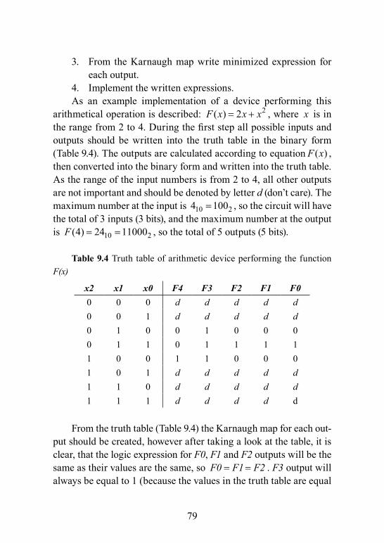
79
3. From the Karnaugh map write minimized expression for each output.
4. implement the written expressions.As an example implementation of a device performing this
arithmetical operation is described: 2( ) 2F x x x= + , where x is in the range from 2 to 4. During the first step all possible inputs and outputs should be written into the truth table in the binary form (table 9.4). the outputs are calculated according to equation ( )F x , then converted into the binary form and written into the truth table. As the range of the input numbers is from 2 to 4, all other outputs are not important and should be denoted by letter d (don’t care). the maximum number at the input is 10 24 100= , so the circuit will have the total of 3 inputs (3 bits), and the maximum number at the output is 10 2(4) 24 11000F = = , so the total of 5 outputs (5 bits).
table 9.4 truth table of arithmetic device performing the function F(x)
x2 x1 x0 F4 F3 F2 F1 F00 0 0 d d d d d0 0 1 d d d d d0 1 0 0 1 0 0 00 1 1 0 1 1 1 11 0 0 1 1 0 0 01 0 1 d d d d d1 1 0 d d d d d1 1 1 d d d d d
From the truth table (table 9.4) the Karnaugh map for each out-put should be created, however after taking a look at the table, it is clear, that the logic expression for F0, F1 and F2 outputs will be the same as their values are the same, so F0 F1 F2= = . F3 output will always be equal to 1 (because the values in the truth table are equal

80
to 1), so =1F3 . From further analysis of the truth table it is clear that outputs F0, F1 and F2 are the same as input x0: = = =F0 F1 F2 x0 , and output F4 is the same as input x2: =F4 x2 . the full circuit with connected word generator and decoded seven segments indicators is presented in Fig. 9.5. the high level on F3 could be achieved by either connecting the power supply positive voltage or an inverter with a grounded input. Also the number of outputs is greater than the number of inputs of the decoded seven segment indicator, so additional decoded seven segment indicator is used to display the additional bits in the hexadecimal system (4 positions in binary are converted into 1 position in hexadecimal system. the binary output made of 5 bits will need 2 positions in hexadecimal system).
Fig. 9.5 implementation of function F(x)
Other example is an implementation of the arithmetical ope-ration described by this function: ( , ) 2 4F a b a b= + , where a is in range from 0 to 2 and b is in the range from 1 to 3. in this case two input variables are used. maximum number at the input a is
10 22 10= , so the circuit will have 2 inputs (2 bits) for input a and 2 inputs ( 10 23 11= ) for input b . maximum value of the func-tion when 2a = and 3b = is 10 2(2,3) 16 10000F = = , so the total

81
of 5 outputs (5 bits). the values of the function when at least one of the inputs is outside the limits are not important, so they are de-noted as don’t care outputs. usually the truth table may be simpli-fied (Table 9.5) by denoting the other input’s values as x (irrelevant) when at least one input is outside the limits.
From the truth table it is clear that F0 all the time is equal to 0: F0 = 0 and F1 is equal to a0, so Karnaugh maps for F0 and F1 are not needed. For F2, F3 and F4 Karnaugh maps (Fig. 9.6) should be created because it is not clear at first sight what expression they will have. From Karnaugh maps expressions could be written: F2 a1b0 a1b0 a1 b0= + = ⊕ ; F3 a1b1 a1b1 b0 a1 b1 b0= + + = ⊕ + ; F4 a1b1b0= . Function implementation is shown in Fig. 9.7.
table 9.5 truth table of arithmetic device performing function F(a,b)
a1 a0 b1 b0 F4 F3 F2 F1 F0x x 0 0 d d d d d0 0 0 1 0 0 1 0 00 0 1 0 0 1 0 0 00 0 1 1 0 1 1 0 00 1 0 1 0 0 1 1 00 1 1 0 0 1 0 1 00 1 1 1 0 1 1 1 01 0 0 1 0 1 0 0 01 0 1 0 0 1 1 0 01 0 1 1 1 0 0 0 01 1 x x d d d d d
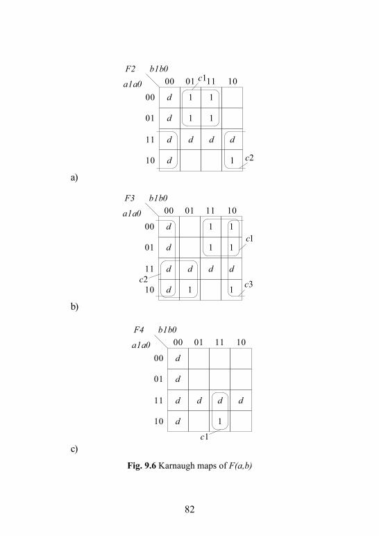
82
a)
d
00
d
1
1
1
1
01 11 10b1b0
a1a0
d
d d d
1
d
00
01
11
10
F2c1
c2
b)
d
00
d
1
1
1
1
01 11 10b1b0
a1a0
d
d
1
d d
1
d
00
01
11
10
F3
c2
c1
c3
c)
d
00
d
01 11 10b1b0
a1a0
d
d d
1
d d
00
01
11
10
F4
c1
Fig. 9.6 Karnaugh maps of F(a,b)

83
Fig. 9.7 implementation of function F(a,b)
tasks
during the laboratory work you will receive different tasks from the tutor.
example of the obligatory tasks (for 6 points out of 10 pos-sible):
1. From any number of 2nAnd logic gates and inverters de-sign a half-adder circuit. implement the circuit and show its operation to the tutor. (2 points)
2. design and implement the circuit performing this arithmet-ical function: 2( ) 3F x x= + , where x is in the range from 1 to 4. show its operation to the tutor. (4 points)

84
example of the additional task (4 points):3. From any logic gates design an arithmetic device with three
inputs A, B and C and one output F which is equal to zero when the number of zeros at the inputs is even. show the results to the tutor.
Control questions
1. explain the operation of half-adder.2. explain the operation, differences and similarities of full
adder and full subtractor.3. Perform necessary calculations and design a circuit per-
forming this function: ( ) 2 3F x x= + , where x is 0, 1, 2, 3. 4. how many bits would be needed for inputs and outputs of
function ( ) 3 3F x x= + , where x is in the range from 3 to 6?
Literature
1. Kleitz, W. (2008). Digital Electronics: A Practical Ap-proach. mcGraw hill, p. 222–228, 238–234.
2. lala, Parag, K. (2007). Principles of Modern Digital De-sign. A John Willey & sons inc., p. 125–135.
3. Kirvaitis, r. (2000). Digital Devices. E-Text-book. Avail-able from the author, p. 52–56.
4. Kirvaitis, r. (1999). Loginės schemos. Vilnius: enciklope-dija, p. 108–120. (in lithuanian)

85
10. Gate LeVeL DesiGn oF otHeR CombinationaL LoGiC DeViCes
objective
the goal of this work is to learn how to design other combina-tional logic devices from any logic gates and how to use manufac-tured ic devices for this purpose.
theory
multiplexers and Demultiplexers
sometimes it is necessary to use the same signal line of the cir-cuit for signals from different logic devices. in this case a fast, con-trollable by logic signals switch is needed. such switch is known as multiplexer (Fig. 10.1 a, c). it is a device made of logic gates which can send a signal from any input line i, selected by address s to an output line.
dmuX d0
d1
s0
In0muX
s0
i0
i1Out
a) b)

86
i0i1
Outi2i3
muX
s0 s1
d0d1
In0d2d3
dmuX
s0 s1
c) d) Fig. 10.1 a) 2-to-1 and c) 4-to-1multiplexers, b) 1-to-2 and d) 1-to-4
demultiplexers
Another device is demultiplexer (Fig. 10.1 b, d), which is also an electronic switch. demultiplexer sends an input signal to any out-put data line d, selected by address s.
to understand the operation of the multiplexer it is necessary to start with simple 2-to-1 multiplexer and analyze its simplified truth table (table 10.1). selector input s0 selects one of the two inputs i1 or i0. Only the inputs selected by s0 are important, that’s why the inputs which are not selected are denoted by x (irrelevant). this way the multiplexer’s logic function could be written straight from the truth table by writing out the minterms where the function is equal to 1 and adding them: +Out s0 i0 s0 i1= ⋅ ⋅ .
table 10.1 truth table of 2-to-1 multiplexer
i1 i0 s0 Outx 0 0 00 x 1 0x 1 0 11 x 1 1

87
table 10.2 truth table of 1-to-2 demultiplexer
In0 s0 d1 d00 0 0 00 1 0 01 0 0 11 1 1 0
A similar situation is with the demultiplexer. however 1-to-2 demultiplexer has 2 outputs, so 2 expressions should be written. the truth table (Table 10.2) is filled with 1s only when the input is 1 and the selector s0 points into the output of interest. Again the logic functions for the demultiplexer could be written by writing out the minterms where the outputs are equal to 1. in the case of demulti-plexer, there will be just one minterm for each output: d0 In0 s0= ⋅ , d1 In0 s0= ⋅ .
table 10.3 truth table of 4-to-1 multiplexer
i3 i2 i1 i0 s1 s0 Outx x x 0 0 0 0x x 0 x 0 1 0x 0 x x 1 0 00 x x x 1 1 0x x x 1 0 0 1x x 1 x 0 1 1x 1 x x 1 0 11 x x x 1 1 1

88
Fig. 10.2 4-to-1 multiplexer
A more complex is 4-to-1 multiplexer. the signal from the se-lected input is being passed to the output. signals on the not selected inputs are irrelevant and are denoted by x (table 10.3). An expres-sion could be written by writing out the minterms where the output is equal to 1: + + +Out i0 s1 s0 i1 s1 s0 i2 s1 s0 i3 s1 s0= ⋅ ⋅ ⋅ ⋅ ⋅ ⋅ ⋅ ⋅ . the circuit is shown in Fig. 10.2.
expressions of the demultiplexer are also written from the truth table where the outputs are equal to 1 (table 10.4): d0 In0 s1 s0= ⋅ ⋅ , d1 In0 s1 s0= ⋅ ⋅ , d2 In0 s1 s0= ⋅ ⋅ , d3 In0 s1 s0= ⋅ ⋅ . the circuit is presented in Fig. 10.3.

89
table 10.4 truth table of 1-to-4 demultiplexer
In0 s1 s0 d3 d2 d1 d00 0 0 0 0 0 00 0 1 0 0 0 00 1 0 0 0 0 00 1 1 0 0 0 01 0 0 0 0 0 11 0 1 0 0 1 01 1 0 0 1 0 01 1 1 1 0 0 0
79
equal to 1: + + +Out i0 s1 s0 i1 s1 s0 i2 s1 s0 i3 s1 s0= ⋅ ⋅ ⋅ ⋅ ⋅ ⋅ ⋅ ⋅ . the cir-cuit is shown in Fig. 10.2.
expressions of demultiplexer are also written from the truth ta-ble where the outputs are equal to 1 (table 10.4): d0 In0 s1 s0= ⋅ ⋅ , d1 In0 s1 s0= ⋅ ⋅ , d2 In0 s1 s0= ⋅ ⋅ , d3 In0 s1 s0= ⋅ ⋅ . the circuit is presented in Fig. 10.3.
table 10.4 truth table of 1-to-4 demultiplexer
In0 s1 s0 d3 d2 d1 d00 0 0 0 0 0 0 0 0 1 0 0 0 0 0 1 0 0 0 0 0 0 1 1 0 0 0 0 1 0 0 0 0 0 1 1 0 1 0 0 1 0 1 1 0 0 1 0 0 1 1 1 1 0 0 0
Fig. 10.3 1-to-4 demultiplexer Fig. 10.3 1-to-4 demultiplexer
it is possible to stack the multiplexers and demultiplexers. this way it is possible to design a large multiplexer from the smaller ones. For example, it is possible to make 4-to-1 multiplexer from three 2-to-1 (Fig. 10.4 a) or 8-to-1 from seven 2-to-1 multiplexers. the same is true for demultiplexers, it possible to make 1-to-4 de-multiplexer from three 1-to-2 demultiplexers (Fig. 10.4 b).

90
a)
MUXi0
i1
MUXi2
i3
MUX Out
s0 s1b)
DMUXIn0
DMUX d0
d1
DMUX d2
d3
s0 s1
Fig. 10.4 a) 4-to-1 multiplexer b) 1-to-4 demultiplexer
Code Converters, encoders and Decoders
code converters transform one code at input to another code at output. For example, binary is transformed to Gray or Gray code to binary. encoder encodes signal in every of 2n inputs into individual n bits code at output. the operation of decoder is opposite; it trans-forms n bits code at the input into signal on one of its 2n outputs. For example, every key press on the keyboard is encoded by encoder into the binary code at its output. design of an encoder or decoder is performed in a similar way as arithmetical devices. A demultiplexer with high constant signal applied at the input could be seen as a sim-ple decoder, which decodes the binary address and sets the relative input high. An example will be presented in the next section.
91
methodology
the design of encoder or decoder is done following the same steps as presented in the previous work. As an example 4-to-2 en-coder is implemented. this encoder should display the address of the input active (of course, only one input could be active at the same time and at any time there should be just one input which is always active). the encoder has 4 inputs and 2 outputs to encode all 4 inputs. Now the truth table could be filled (Table 10.5), denoting all not important outputs as d and all other combinations of inputs as x (irrelevant). Karnaugh maps (Fig. 10.5) could be filled from the truth table.
table 10.5 truth table of 4-to-2 encoder
i3 i2 i1 i0 a1 a0x x x x d d0 0 0 1 0 00 0 1 0 0 10 1 0 0 1 01 0 0 0 1 1
Here few minimization possibilities exist, the first one is to use one contour to include all 1s (Fig. 10.5 a, b): a1 i1 i0= ⋅ , a0 i2 i0= ⋅ ; or to use two contours (Fig. 10.5 c, d): +a1 i2 i3= , +a0 i1 i3= . the choice depends on the situation. In this case the first choice is bet-ter as all inputs are inverted and by the use of de morgan theorem And gates are easily converted into standard nOr gates. From the first case expressions it is clear that input i3 is not used, so it shouldn’t be connected in any way to the output.
now the circuit could be implemented (Fig. 10.6). in order to show the operation of the circuit, the “shift left” pattern should be selected in the word generator, so that only one output is active at a

92
time. By pressing “step” button the decoded seven segment indica-tor should show the number of the input active.
a)
1
00
d
d
0
d
d
d
0
01 11 10i1 i0
i3 i2
1
d
d
d
d
d
d
d
00
01
11
10c1
a1
b)
i3 i2
0
00
d
d
0
d
d
d
1
01 11 10i1 i0
1
d
d
d
d
d
d
d
00
01
11
10c1
a0
c)
1
00
d
d
0
d
d
d
0
01 11 10i1 i0
i3 i2
1
d
d
d
d
d
d
d
00
01
11
10c2
c1
a1
d)
i3 i2
0
00
d
d
0
d
d
d
1
01 11 10i1 i0
1
d
d
d
d
d
d
d
00
01
11
10c2
c1a0
Fig. 10.5 Karnaugh maps of 4-to-2 encoder
Fig. 10.6 connection of 4-to-2 encoder
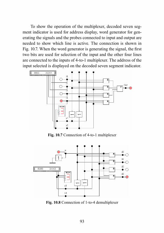
93
to show the operation of the multiplexer, decoded seven seg-ment indicator is used for address display, word generator for gen-erating the signals and the probes connected to input and output are needed to show which line is active. the connection is shown in Fig. 10.7. When the word generator is generating the signal, the first two bits are used for selection of the input and the other four lines are connected to the inputs of 4-to-1 multiplexer. the address of the input selected is displayed on the decoded seven segment indicator.
Fig. 10.7 connection of 4-to-1 multiplexer
Fig. 10.8 connection of 1-to-4 demultiplexer

94
similar connection is required to show the operation of the de-multiplexer (Fig. 10.8). in this case the constant high level signal is applied to the demultiplexer’s input and the demultiplexer is work-ing as a decoder, by activating the probe at output d, according to the address supplied via the address select lines s from the word generator.
A lot of components like basic logic gates, latches, multiplexers, demultiplexers, encoders, decoders and many others are implement-ed as integrated circuits (ic) devices. ic device may include one or more components inside. to make the ic work, it is necessary to connect the power supply (usually 5 V if not otherwise stated in the datasheet) to Vcc pin and ground to Gnd pin. in the case of 4xxx cmOs device the power supply (in electronics Workbench simu-lation environment it is usually 15 V, in multisim it could be 5 V, 10 V or 15 V) should be connected to Vdd pin and ground to Vss pin. connection of other pins should be checked in the datasheet or help file. Usually the truth table of the device is provided and from it the connection is determined. Often the structure of the basic logic gates ic could be determined from the name of the ic. For example, 4081 ic has the name “Quad 2-in And”. From this name it is clear that ic includes four And logic gates with two inputs each. the connection of the pins of each And logic gate could be determined from the pins’ names. 4081 ic has four pins which name starts with letter “O” – those are the outputs; eight pins have names starting with letter “i” – those are the inputs. now it could be assumed that pins I1, I2 and O1 belong to the first AND logic gate; pins I3, I4 and O2 – to the second and so on.
As an example connection of 8-to-3 priority encoder 74148 ic is shown in Fig. 10.9. According to the truth table from the help file of a modelling program (table 10.6) the encoder inputs are from 7 to 0 and encoded signal outputs are from A0 to A2. Also it is important to note, that the word generator was connected through the invert-ers as “shift left” pattern outputs 1 and in our case 0 is necessary to
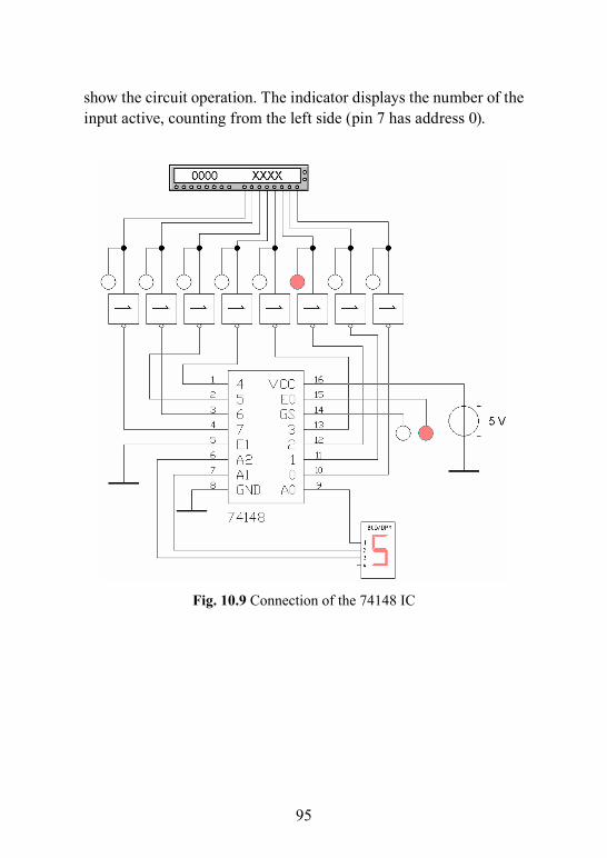
95
show the circuit operation. the indicator displays the number of the input active, counting from the left side (pin 7 has address 0).
Fig. 10.9 connection of the 74148 ic

96
table 10.6 truth table of 74148 ic
EI 0 1 2 3 4 5 6 7 A1 A1 A0 GS EO1 x x x x x x x x 1 1 1 1 10 1 1 1 1 1 1 1 1 1 1 1 1 00 x x x x x x x 0 1 0 0 0 10 x x x x x x 0 1 1 1 1 0 10 x x x x x 0 1 1 1 1 1 0 10 x x x x 0 1 1 1 1 1 1 0 10 x x x 0 1 1 1 1 1 1 1 0 10 x x 0 1 1 1 1 1 1 1 1 0 10 x 0 1 1 1 1 1 1 1 1 1 0 10 0 1 1 1 1 1 1 1 1 1 1 0 1
tasks
during the laboratory work you will receive different tasks from the tutor.
example of the obligatory tasks (for 6 points out of 10 pos-sible):
1. design a decoder that converts binary numbers (0, 1, 2, 3, 4, 5) into a filling code (00000, 00001, 00011, 00111, 01111, 11111). implement the circuit, show its operation and an-swer the tutor’s questions. (3 points)
2. design a 1-to-4 demultiplexer, implement the circuit, show its operation and answer the tutor’s questions. (3 points)
example of the additional task (4 points):3. investigate 74251 ic (8-to-1 multiplexer). connect all ne-
cessary power supplies, instruments and indicators to show its operation to the tutor.
97
Control questions
1. explain the operation of the multiplexer and demultiplex-er.
2. Perform the necessary calculations and design a 3-to-2 en-coder. When all the inputs are zeros the output should also be zero. When the first input is active the output should be 01, when the second – 10, when the third – 11.
3. design a 2-to-1 multiplexer and 1-to-2 demultiplexer.
Literature
1. Kleitz, W. (2008). Digital Electronics: A Practical Ap-proach. mcGraw hill, p. 264–301.
2. lala, Parag, K. (2007). Principles of Modern Digital De-sign. A John Willey & sons inc., p. 117–124.
3. Kirvaitis, r. (2000). Digital Devices. E-Text-book. Avail-able from the author, p. 59–65.
4. Kirvaitis, r. (1999). Loginės schemos. Vilnius: enciklope-dija, p. 120–128. (in lithuanian)

98
11. CombinationaL LoGiC iC DeViCes
objective
the goal of this work is to get acquainted with the combina-tional logic IC devices and to learn how to apply them for definite tasks.
theory
integrated circuits (ic) devices are more convenient to ap-ply than discrete components; they have advantages of taking less space, consuming less power and easier to work with. combina-tional logic ic devices are divided into the families by the technolo-gy used. One large family is ttl and the name of ic usually starts with 74xx and another large family is cmOs with the usual name starting with 4xxx. Keep in mind that the name of ic starting with 74 and continued with letters is not necessary of ttl type. For ex-ample, the devices having letter c in the name like 74cxx, 74hcxx are cmOs compatible with ttl, ic having letter B like 74ABtxx, 74ABthxx are BicmOs compatible with ttl. Other letters usu-ally denote modifications in the structure. For example, letter L are for low voltage or low power, letter h denotes high-speed opera-tion. A simple ttl ic 7420 (Fig. 11.1) has two 4nAnd gates in-side based on ttl technology and 4002 has two 4nOr gates inside based on cmOs technology. the choice of the technology depends on requirements.

99
87
11. CombinationaL LoGiC iC DeViCes
objective
the goal of this work is to get acquainted with the combination-al logic ic devices and learn how to apply them for definite tasks.
theory
integrated circuits (ic) devices are more convenient to apply than discrete components; they have advantages of taking less space, consuming less power and easier to work with. combinational logic ic divided into the families by the technology used. One large family is ttl and the name of the ic usually starts with 74xx and another large family is cmOs with the usual name starting with 4xxx. Keep in mind that the name of the ic starting with 74 and continued with letters is not necessary of ttl type. For example, the devices having letter c in the name like 74cxx, 74hcxx are cmOs compatible with ttl, ic having letter B like 74ABtxx, 74ABthxx are BicmOs compatible with ttl. Other letters usually denotes modifications in structure. For example letter l are for low voltage or low power, letter h denotes high-speed operation. A simple ttl ic 7420 (Fig. 11.1) has two 4nAnd gates inside based on ttl technology and 4002 has two 4nOr gates inside based on cmOs technology. the choice of the technology depends on requirements.
a) b)
&&
7420
12
c)
&
&
Fig. 11.1 7420 ic a) pinout b) internal structure c) graphical symbol a) b)
&&
7420
12
c)
&
&
Fig. 11.1 7420 ic a) pinout b) internal structure c) graphical symbol
usually the type of the gates in the design depends on the avail-able ic. if nAnd ic are used then all non-nAnd gates should be converted into a nAnd type, if nOr ic are used, then all non-nOr gates should be converted into a nOr type. the conversion is done by changing the gate into the required type and then inverters are added and / or removed until the required operation is restored. typical line conversions (Fig. 11.2) are used when dealing with gate conversion.
1≡
1≡
1≡
1≡
≡
≡
Fig. 11.2 line conversions

100
Gate type conversion is performed via de morgan’s theorem: A B A B⋅ = + , A B A B+ = ⋅ (Fig. 11.3). inverter could be created from nAnd or nOr gate simply by connecting a non-needed in-puts to power supply for nAnd gate or to the ground in the case of nOr gate. An inverter made by connecting the inputs together is not recommended due to the increased load on the previous gate’s output circuit and due to the increased load capacitance which will have an impact on the speed of operation.
& 1≥≡
&1≥≡
Fig. 11.3 Basic logic gate conversions
methodology
implementation of the circuit from ic devices is explained in the example.
the minimized expression F A B C= + + should be implement-ed using NAND TTL IC 7420. The first step is to change all the gates into nAnd type used by 7420 ic. it could be done by applying de morgan’s theorem directly on expression F A B C A B C= + + = ⋅ ⋅ or from the circuit (Fig. 11.4). After the circuit is in nAnd form, it is possible to implement it using the standard ic (Fig. 11.5).

101
a) b)Fig. 11.4 Function a) initial b) made of nAnd gates and inverters
89
methodology
the implementation of the circuit from the ic devices is ex-plained on example.
the minimized expression F A B C= + + should be implement-ed using nAnd ttl ic 7420. the first step is to change all the gates into the nAnd type used by 7420 ic. it could be done by ap-plying de morgan’s theorem directly on expression F A B C A B C= + + = ⋅ ⋅ or from the circuit (Fig. 11.3). After the circuit is in nAnd form, it is possible to implement it using the standard ic (Fig. 11.4).
a) b)Fig. 11.3 Function a) initial b) made of nAnd gates and inverters
Fig. 11.4 F(A,B,C) implemented via the 7420 ic
From the Fig. 11.1 it is known, that 7420 ic includes two 4nAnd logic gates. the inputs of the first gate are denoted with number and letters: 1A, 1B, 1c, 1d. the output of the first gate is
Fig. 11.5 F(A,B,C) implemented via 7420 ic
From Fig. 11.1 it is known, that 7420 ic includes two 4nAnd logic gates. The inputs of the first gate are denoted with numbers and letters: 1A, 1B, 1C, 1D. The output of the first gate is denoted by 1Y. the same is true for the second gate with the only difference that the inputs and output are denoted with number 2. Pins with nc notation internally are not connected.
Function inputs A and B could be directly connected to the se-cond 4nAnd gate of 7420 ic. input C should be inverted. As only the second 4NAND gate is used in the calculation, the first one could be used as an inverter by supplying signal C to one of the inputs 1d and connecting all other unused input pins to the power supply. in-

102
verted signal C from the output 1Y then connected to the second 4nAnd gate via 2A pin. Because 3nAnd operation is needed and the gate is 4nAnd, unused 2d pin is connected to power supply. the function output is 2Y. logic converter or word generator to-gether with the logic analyzer could be directly connected to check if the function was implemented correctly.
When connecting ic it is necessary to choose the right power supply voltage as ttl and cmOs may use a different or the same power supply voltage. in the simulation environment the usual pow-er supply voltage for ttl ic is 5 V and is usually denoted as Vcc. For cmOs the supply voltage is denoted as Vdd and in the simula-tion environment it may be 5 V, 10 V or 15 V (Fig. 11.6). Keep in mind that in reality a different power supply voltage may be needed for the ic at hand, so always check the datasheet. Also the check of the logic voltage levels is required to avoid connecting wrong volt-ages to the inputs of the ic.
90
denoted by 1Y. the same is true for the second gate with the only difference that the inputs and output are denoted with number 2. Pins with nc notation internally are not connected.
Function inputs A and B could be directly connected to the se-cond 4nAnd gate of the 7420 ic. input C should be inverted. As only the second 4nAnd gate is used in the calculation, the first one could be used as an inverter by supplying signal C to one of the in-puts 1d and connecting all other unused input pins to the power sup-ply. inverted signal C from the output 1Y then connected to the se-cond 4nAnd gate via the 2A pin. Because 3nAnd operation is needed and the gate is 4nAnd, unused 2d pin is connected to the power supply. the function output is 2Y. logic converter or word generator together with the logic analyzer could be directly connect-ed to check if the function was implemented correctly.
When connecting ic it is necessary to choose the right power supply voltage as ttl and cmOs may use a different or the same power supply voltage. in the simulation environment the usual power supply voltage for ttl ic is 5 V and is usually denoted as Vcc. For cmOs the supply voltage is denoted as Vdd and in the simulation environment it may be 5 V, 10 V or 15 V (Fig. 11.5). Keep in mind that in reality a different power supply voltage may be needed for the ic at hands so always check the datasheet. Also the check of the log-ic voltage levels is also required to avoid connecting wrong voltages to the inputs of the ic.
Fig. 11.5 connection of power supplies Fig. 11.6 connection of power supplies
the analysis of the ic should always start from the datasheet. if datasheet is not available, preliminary ic structure could be de-termined from the name of IC. Further analysis and clarification of the structure is done via the word generator and logic analyzer tools. logic converter could also be used, however due to the small-

103
er number of inputs, larger ic could be analyzed by parts only. it is important to notice, that ic with a different number of inputs may exist under the same name. So it is necessary to confirm that the right ic is being analyzed.
in real life the timing of the input signals is not perfect and the propagation delay of the different parts of the circuit causes signals to be delayed. these delays may introduce logic error. the risk of an error when only one input signal is changing is called logic haz-ard. usually the logic hazard appears during the change of one of the input signals, when due to delays in a circuit a short change of the output to unexpected value may happen. to avoid logic hazards, during minimization of the function it is necessary to check if in Karnaugh map adjacent contours exist. if they are, additional con-tour should be added to include adjacent 1s from adjacent contours (Fig. 11.7). here c2 and c1 are contours from minimization and c3 is the additional contour joining adjacent c1 and c2 to avoid logic haz-ards. so initial minimized function will be: F B C A C= ⋅ + ⋅ , and with additional contour: F B C A C A B= ⋅ + ⋅ + ⋅ .
00
1 1 1
1
01 11 10
0
1
BC
A
c1c2 c3
( , , )F A B C
Fig. 11.7 Karnaugh map with additional contour to avoid logic hazards
104
tasks
during the laboratory work you will receive different tasks from the tutor.
example of the obligatory tasks (for 6 points out of 10 pos-sible):
1. Analyze 7454 ttl ic. draw this ic logic circuit from log-ic gates and graphical symbol. model the circuit and show that the operation of 7454 ic and your circuit are identical. show the results to the tutor. (3 points)
2. using one 7454 ttl ic and another 74xx fam-ily ic, implement the circuit expressed by this function:
( )( , , , ) 3,4,5,7,10,11,14,15F A B C D m= ∑ . Find the best way to show its operation and answer the tutor’s ques-tions. (3 points)
example of the additional task (4 points):3. change the circuit created in task 2 to avoid logic hazards.
show the results to the tutor.
Control questions
1. What does the acronym ic mean?2. draw the internal structure and graphical symbol of
4002 ic device.3. check the functionality of 4009 and 7404 ic devices. draw
internal structures of these devices and explain the differ-ences.
4. Write de morgan theorem in any form.5. design this function F A B C= + + from the minimal num-
ber of 4002 ic devices. implement the circuit and check its operation.
6. implement the given function avoiding logic hazards ( )( , , , ) 0,1,4,5,6,7,14,15F A B C D m= ∑ .

105
Literature
1. Kleitz, W. (2008). Digital Electronics: A Practical Ap-proach. mcGraw hill, p. 48, 51, 184, 190–191, 217, 271, 273, 275–276, 279, 283, 294, 313–314, 317, 335.
2. Kirvaitis, r. (2000). Digital Devices. E-Text-book. Avail-able from the author, p. 66–77.
3. Kirvaitis, r. (1999). Loginės schemos. Vilnius: enciklope-dija, p. 96–107, 128–159 (in lithuanian).

106
12. basiC synCHRonous LatCHes
objective
the goal of this work is to get acquainted with the basic syn-chronous latches, their structure, operation and truth tables.
theory
Latch or a flip-flop is a bistable device which has two stable states only and two outputs complemented to each other. every memory unit usually includes one or more basic latches. memory devices are essential parts of sequential circuits.
a)
1≥
1≥
Q
Q
S
R
b)
&
&
Q
Q
S
R
Fig. 12.1 Basic sr latch made from a) nOr b) nAnd gates
A simple sr latch could be created of cross connected nOr gates (Fig. 12.1 a). nAnd sr latch can be made of nOr latch ap-plying de morgan’s theorem. As the result (Fig. 12.1 b) input and output signals are inverted for the nAnd sr latch. sr latch can store one bit of information as long as both inputs S and R are low for nOr latch and high for nAnd latch. Active input S = 1 will set nOr latch output Q to a high level, active input R = 1 will reset

107
output Q to a low level. Both inputs cannot be high at the same time for nOr or low for nAnd sr latches as it would result in an unex-pected stored value. such combinations of input signals are called invalid or forbidden. the truth table for nOr and nAnd sr latches is presented in table 12.1. the previous latch output is denoted as q and the outputs denoted with the bold font are forbidden because of the invalid signals both in inputs and outputs.
When the power is supplied to the latch and the passive combi-nation of the input signals is active (00 for nOr, and 11 for nAnd), only the delays in the logic gates determine what the output signal will be, so it is important to reset or set the latches after the power was applied.
let’s analyze how nOr sr latch is functioning when the re-set combination (01) is applied at the input. As R input is high, the output Q of the lower nOr will be 0. now both inputs of the upper nOr are low so the upper nOr output will be 1. When the set-ting combination (10) is active exactly the opposite happens. now the upper nOr will have 0 at the output and because both inputs of the lower nOr are low, output Q of the lower nOr will be 1. When both inputs S and R are low nOr latch stays in the same state holding one of the outputs high. When both inputs of nOr latch are active, both nOr logic gates will have a low level output. this situation when both outputs are the same is an indication that the invalid input signal was supplied to the latch. After the invalid input signal is changed to passive one, the race condition starts and the output depends on the delays in the circuit.

108
table 12.1 truth table of nOr and nAnd sr latches
S R Q Q S R Q Q
0 0 q q 0 0 1 1
0 1 0 1 0 1 1 01 0 1 0 1 0 0 1
1 1 0 0 1 1 q q
in many applications the latch should be set or reset synchro-nously with the control signal. nOr and nAnd sr latches with additional synchronization circuits are presented in Fig. 12.2. these latches are named gated latches or clocked latches. the output of the latch can change according to the input signal only when the control or clock signal C is active. the truth table of the gated nOr sr latch is presented in table 12.2. logic symbols of simple sr latch and gated sr latch are presented in Fig. 12.3.
a)
1≥
1≥
Q
Q
S
R
&
&
C
b)
&
&
Q
Q
S
R
&
&
C
Fig. 12.2 Gated latches a) sr nOr b) sr nAnd

109
table 12.2 truth table of gated nOr sr latch
C S R Q Q
0 x x q q
1 0 0 q q1 0 1 0 11 1 0 1 01 1 1 0 0
s
r
s
rc
a) b)Fig. 12.3 logic symbols of a) basic sr latch b) gated sr latch
Gated sr latch is used as the base for the d latch (Fig. 12.4), Reset input of sr latch is connected with Set input through inverter, so d latch has only one data input and that input determines the data to be stored in the latch when control signal C is active. Another improvement over sr latch is that in this situation invalid combina-tions of signals are not possible. the truth table of d latch is pre-sented in table 12.3.

110
&
&
Q
Q
D &
&
C
1
Fig. 12.4 d latch made from the gated nAnd sr latch
table 12.3 truth table of d latch
C D Q Q
0 x q q1 0 0 11 1 1 0
Often the gated latch or flip-flop should be set or reset regard-less of the status of the clock. to perform the asynchronous uncon-ditional reset or set of the latch, the required signal combination should be supplied omitting the latch gate and avoiding conflict with currently active inputs. circuit with an asynchronous unconditional positive Set (also known as Preset) and asynchronous positive Reset (also known as Clear) is inserted between the gate and the latch (Fig. 12.5). Of course, both Set and Reset cannot be active at the same time because only the closest to the latch circuit will have ef-fect (in our case it is Set). When no signal is applied to the Reset and Set inputs, the latch functions normally, because 2And gates with one input set high will repeat the other input at the output and 2Or

111
gates with one input set low will repeat the other input at the output. so when one of the asynchronous inputs is active, the circuit will “disconnect” the gated part from the latch and send the setting or resetting combination of the signals.
s
r
1≥
&1≥
&
1
1&
&
S
R
C
Reset Set
Fig. 12.5 sr gated latch with asynchronous Set and Reset
Flip-flops also have two stable states and like the gated latches are controlled by a clock signal. The difference is that flip-flops are activated by the edge of the clock pulse rather than the level of the clock pulse.
a)
s
rc
s
rc1
1
DC
b)
d
c
c)
s
rc
s
rc
1
DC
1 d)
d
c
Fig. 12.6 D flip-flop a) positive edge triggered b) logic symbol c) pulse-triggered (master-slave) d) logic symbol

112
When speaking about flip-flops two distinctive types exist: pulse-triggered or master-slave and edge triggered. Pulse-triggered flip-flops are designed from two gated latches connected in a master-slave fashion. Such interconnection (Fig. 12.6 c) forces the flip-flop to store the data in the master gated latch during the positive clock signal and output the stored data into the slave gated latch during the transition from the positive to negative clock signal. edge-triggered flip-flops are similar in design to pulse-triggered with the only dif-ference, that the inverter is placed before the gate input of the first gated latch. (Fig. 12.6 a)
a)
s
r
s
rc
1
&
&
J
K
C
b)
J
K
c
Fig. 12.7 Pulse-triggered JK flip-flop a) circuit b) logic symbol
table 12.4 Truth table of JK flip-flop
J K Q Q
0 0 q q
0 1 0 11 0 1 0
1 1 q q

113
For the pulse-triggered flip-flop to work properly first D input should be set and only then the pulse should be supplied to the clock line. changing both inputs at the same time may lead to an unex-pected output as D signal may not be caught.
JK flip-flop (Fig. 12.7) is very similar to SR flip-flop with the added feedback lines from the outputs to the input And gates. in this case the invalid signal combination with both inputs high be-comes a valid combination inverting JK flip-flop output.
a)
s
r
s
rc
1
&
&
T
C
b)
t
c
Fig. 12.8 Pulse-triggered T flip-flop a) circuit b) logic symbol
table 12.5 Truth table of T flip-flop
T Q Q
0 q q
1 q q
JK flip-flop property to invert the output when both J and K inputs are high is used in T flip-flop. Actually T flip-flop is the same JK flip-flop with shorted J and K inputs. (Fig. 12.8) Because T input is just inverting the output, manufactured T flip-flops usually do have asynchronous set and reset inputs.

114
methodology
to avoid race conditions when the circuit simulation is started it is recommended to add a delay switch into the latch (Fig. 12.9), this way the latch will be stabilized before the feedback circuit is con-nected. delay should be set to 0.001 s or shorter from the delayed switch context menu to make sure that the latch is stabilized during one clock of word generator (word generator’s typical frequency is 1 khz). Another possibility is to provide a setting or resetting com-bination during the start of the simulation. Adding a delay switch may be helpful in a situation where it is not possible to apply setting or resetting combination to all latches at once, especially in flip-flops.
Fig. 12.9 nOr sr latch with delay switch
during the simulation the input signals should be carefully se-lected to avoid invalid combinations as it will cause the latch to os-cillate. The best way is to fill the word generator manually, changing one signal at a time. sometimes the input signals should be control-led independently by a switch, for example, for asynchronous set and reset. in such situation a combination of the word generator, switches and logic analyzer is possible.

115
tasks
during the laboratory work you will receive different tasks from the tutor.
example of the obligatory tasks (for 6 points out of 10 pos-sible):
1. From 2nAnd logic gates and inverters design a gated d latch. draw the timing diagrams to show the operation of the gated latch. show the results to the tutor. (3 points)
2. using standard sr latch and other logic gates design the gated d latch with unconditional asynchronous PR (Preset) input. When the Preset is not active, the latch should work normally, when the PR is active, the latch should be set ( 1Q = ; 0Q = ). test the circuit, draw the timing diagrams and show the results to the tutor. (3 points)
example of the additional task (4 points):3. change the circuit created in task 2 by adding uncondi-
tional asynchronous CLR (Clear) input. during simulation keep in mind that both PR and CLR signals cannot be active at the same time. test the circuit, draw the timing diagrams and show the results to the tutor.
Control questions
1. explain the differences between the latch, gated latch and flip-flop.
2. What are the setting combinations for sr latches made of nAnd logic gates and nOr logic gates?
3. What are the invalid combinations for sr latches made of nAnd and nOr logic gates?

116
4. draw the gated sr latch circuits made of nAnd and nOr logic gates. test if both circuits are operating correctly and fill in their truth tables.
5. draw the gated d latch circuit and explain its operation.6. Add inverted unconditional asynchronous Preset and Clear
inputs to the gated d latch and explain their operation.7. Draw positive edge triggered D flip-flop circuit and pulse-
triggered (master-slave) D flip-flop circuit, explain their operation and differences. implement both circuits using standard sr latches and draw their timing diagrams.
8. Draw positive edge triggered JK flip-flop and positive edge triggered T flip-flop circuits, explain their operation and differences, draw timing diagrams.
Literature
1. Kleitz, W. (2008). Digital Electronics: A Practical Ap-proach. mcGraw hill, p. 370–413.
2. lala, Parag, K. (2007). Principles of Modern Digital De-sign. A John Willey & sons inc., p. 157–167.
3. Kirvaitis, r. (2000). Digital Devices. E-Text-book. Avail-able from the author, p. 78–81.
4. Kirvaitis, r. (1999). Loginės schemos. Vilnius: enciklope-dija, p. 160–198. (in lithuanian)
117
13. ReGisteRs
objective
the goal of this work is to master the register’s types, their structure and operation.
theory
One flip-flop stores one bit of information. When a set of n flip-flops is used to store n bits of data, this set is referred to as a register. registers are designed to hold data. registers may be clas-sified based on their clock synchronization, internal structure, way the data is stored and retrieved. data storage and retrieval registers could be divided into parallel, when the data is transferred n bits at the same time, serial or shift when data is transferred 1 bit at a time and a parallel-access shift registers a universal type which can work as a parallel and as a serial register with data conversion ability. in parallel-access shift registers the data could be converted from parallel to serial when n bits are stored at the same time and then retrieved 1 bit at a time or from serial to parallel where n bits are stored 1 bit at a time and then retrieved n bits at the same time.
Basic 4 bits parallel register made of gated d latches is shown in Fig. 13.1. All d latches are connected to the same control line. Writing process is performed by setting the data bits on D inputs and setting the control line from low to high and back to low. the reading could be performed at any time when the write operation is not in progress.

118
d
c
d
c
d
c
d
cC
D0 Q0 D1 Q1 D2 Q2 D3 Q3
Fig. 13.1 4 bit basic parallel register made from gated d latches
In the basic 4 bits serial register (Fig. 13.2) one D flip-flop is used to store one bit of information. edge-triggered or pulse trig-gered D flip-flops are connected in series, so the data at the output of the first flip-flop is supplied to the input of the second flip-flop. this way with each positive edge of the clock the data is shifted to the next flip-flop. Eventually, after four positive edges of the clock, the first supplied bit will be available at the output iD of the register and with other three positive edges of the clock the remaining three bits of the data will be received at the output.
d
c
d
c
d
c
d
cC
D i+4 D i
Fig. 13.2 Basic 4 bit serial register made from edge-triggered D flip-flops
Parallel-access shift register (Fig 13.3) can work as parallel or serial register. such operation is possible due to 2-to-1 multiplexers inserted between input signal and flip-flops. When input S is high the multiplexer is directing output Q to input D of the next flip-flop and the circuit is working as a serial register. When input S is low the circuit is working as a parallel register. Parallel-access register could be used as data converter from the serial to parallel and from

119
the parallel to serial. When signal S is low, the register could be loaded with the data in parallel way and then, by setting S high, the data could be received in a serial way and vice versa.
d
cC
D0
muX
Q0
d
c
muX
D1 Q1
d
c
muX
D2 Q2
D i+3
D i
S
Fig. 13.3 3 bit parallel-access shift register
methodology
to show the operation of the register it is necessary to prepare the data to be written into the register. such data could be entered into the word generator and then supplied to the circuit. logic ana-lyzer should be connected to the inputs and outputs of the circuit to monitor the changes.
in Fig. 13.4 2 bit parallel register made of JK negative edge triggered flip-flops is shown. Inputs J are connected through the inverters to inputs K, so JK flip-flop is working as a D flip-flop. Positive asynchronous inputs S and R are shorted to the ground to prevent any ambiguous signals on them. inverter, added to the clock line, forces the register to store information on the positive edge while using negative edge triggered flip-flops. Word generator is filled with the “Up counter” pattern and the clock is connected to the rightmost pin of word generator which is the most frequently changing with the selected pattern. the timing diagram (in our case the output of the logic analyzer) after 12 steps is shown in Fig. 13.5. From the timing diagram it is clear that during the positive edge of the clock, data signals are stored into the flip-flops.
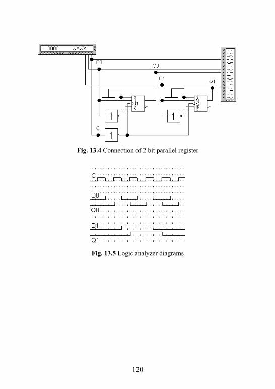
120
106
Methodology
To show the operation of the register it is necessary to prepare the data to be written into the register. Such data could be entered into the word generator and then supplied to the circuit. Logic ana-lyzer should be connected to the inputs and outputs of the circuit to monitor the changes.
In Fig. 13.4 2 bit parallel register made of JK negative edge trig-gered flip-flops is shown. Inputs J are connected through the invert-ers to inputs K, so JK flip-flop is working as a D flip-flop. Positive asynchronous inputs S and R are shorted to the ground to prevent any ambiguous signals on them. Inverter, added to the clock line, forces the register to store information on the positive edge while using negative edge triggered flip-flops. Word generator is filled with the “Up counter” pattern and the clock is connected to the rightmost pin of word generator which is the most frequently changing with the selected pattern. The timing diagram (in our case the output of the logic analyzer) after 12 steps is shown in Fig. 13.5. From the timing diagram it is clear that during the positive edge of the clock, data signals are stored into the flip-flops.
Fig. 13.4 Connection of the 2 bit parallel register Fig. 13.4 connection of 2 bit parallel register
Fig. 13.5 logic analyzer diagrams

121
tasks
during the laboratory work you will receive different tasks from the tutor.
example of the obligatory tasks (for 6 points out of 10 pos-sible):
1. From d gated latches design a 3 bit parallel register. con-nect the necessary indicators and tools to show the opera-tion of the circuit. draw timing diagrams and show the re-sults to the tutor. (3 points)
2. From D flip-flops design two 3 bit serial registers. Connect them in series and explain how many clock pulses are need-ed to transfer the data from one register to other. connect the necessary indicators and tools to show the operation of the circuit. draw timing diagrams and show the results to the tutor. (3 points)
example of the additional task (4 points):3. design a 2-to-1 multiplexer. From the 2-to-1 multiplexers
and D flip-flops design a 3 bit parallel-access shift register. connect the necessary indicators and tools to show the op-eration of the circuit in parallel and serial modes. show the results to the tutor.
Control questions
1. What is the difference between serial and parallel regis-ters?
2. What types of flip-flops are preferable for serial registers and why?
3. explain the operation of the serial 3 bit register and draw its timing diagrams.

122
4. how many clock cycles are needed to pass one bit from the input to the output of 5 bit serial register?
5. draw the circuit of 2-to-1 multiplexer.6. What for multiplexers are used in parallel-access shift reg-
ister?7. explain the operation of 3 bit parallel-access shift register.8. Design D type flip-flop from JK flip-flop. Test the opera-
tion of the designed flip-flop.9. design 2 bit serial register and draw its timing diagrams.10. design 2 bit parallel-access shift register. load it in paral-
lel way and output the loaded data in serial way. how many clock cycles are needed to output the stored data from the designed register? draw its timing diagrams showing the load and output operations.
Literature
1. Kleitz, W. (2008). Digital Electronics: A Practical Ap-proach. mcGraw hill, p. 374, 398, 542–563.
2. lala, Parag, K. (2007). Principles of Modern Digital De-sign. A John Willey & sons inc., p. 322–331.
3. Kirvaitis, r. (2000). Digital Devices. E-Text-book. Avail-able from the author, p. 100–104.
4. Kirvaitis, r. (1999). Loginės schemos. Vilnius: enciklope-dija, p. 199–203. (in lithuanian)

123
14. CounteRs
objective
the goal of this work is to get acquainted with binary counters, their structure and operation.
theory
counter is a special arithmetic circuit used for the purpose of counting pulses. to keep the counting value, the counter uses flip-flops in a similar way as a serial register. However in the case of a counter special type of counting D, T or JK flip-flops are pref-erable because of their ability to change the state into opposite on the positive pulse in their inputs. counters can work as up coun-ter, down counter or universal counter which can count in both directions. Asynchronous inputs of the flip-flops could be used to load the initial value into the counter. two distinctive types of counters exist: ripple, or asynchronous, counters and synchronous counters.
ripple counter is the simplest counter made as serial connec-tion of flip-flops only. In a 3 bit ripple counter (Fig. 14.1 a, b) a con-stant high level is applied to all T flip-flops, so they are working as counting T flip-flops. Positive output Q of the flip-flops is used as an output of binary bit. in a ripple up counter (Fig. 14.1 a) the inverted output is serving as a clock input to the next T flip-flop and in a ripple down counter (Fig. 14.1 b) the positive output is serving as a clock input to the next flip-flop. The ripple counter has one disad-vantage that the toggling of the flip-flop will happen only after the previous flip-flop has changed its state. This will lead to the output delay equal to the sum of all connected in series flip-flop delays. this delay limits the operational speed of the counter and the work

124
of such a counter is rather asynchronous especially when quantity of bits (and flip-flops) is great.
in the synchronous counters (Fig. 14.1 c, d and Fig. 14.2) all the flip-flops are clocked at the same time from the same source. So the circuit output will be delayed by one flip-flop delay time only. It is also possible to make a universal counter able to count in both direc-tions (Fig. 14.4). this 3 bit counter uses multiplexers at the output of the flip-flops to control the counting direction. When the low level is applied to Up input, the multiplexers conduct positive output Q of T flip-flops, when the high level is supplied – the inverted output of T flip-flop is conducted.
a)
t
c
t
c
t
c
Q0 Q1 Q2
1
C
b)
t
c
t
c
t
c
Q0 Q1 Q2
1
C
c)
t
c
t
c
&
t
c
Q0 Q1 Q2
1
C
&
t
c
Q3

125
d)
t
c
t
c
&t
c
Q0 Q1 Q2
1
C
&t
c
Q3
Fig. 14.1 a) 3 bit ripple up counter b) 3 bit ripple down counter c) synchronous 4 bit up counter d) synchronous 4 bit down counter
t
cmuX
&
Q1
t
c
Q2
t
c
Q0
1
C
muX
Up
Fig. 14.2 synchronous 3 bit up / down counter
methodology
design of a custom counter starts in a similar way as of any sequential circuit:
1. describe sequential circuit, its inputs and outputs.2. draw a state diagram for the expected circuit operation.3. Fill in a next-state table from a state diagram.4. Choose flip-flop and fill in its transition table.5. Fill Karnaugh maps for each flip-flop input from next-state
table and flip-flop transition table.6. Get minimized expressions of the circuit and implement it.
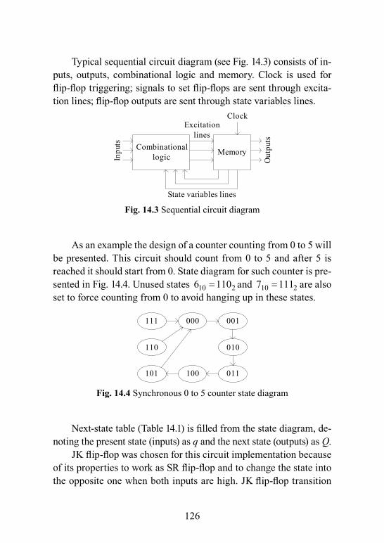
126
typical sequential circuit diagram (see Fig. 14.3) consists of in-puts, outputs, combinational logic and memory. clock is used for flip-flop triggering; signals to set flip-flops are sent through excita-tion lines; flip-flop outputs are sent through state variables lines.
combinationallogic memory
inpu
ts
Out
puts
state variables lines
excitation lines
clock
Fig. 14.3 sequential circuit diagram
As an example the design of a counter counting from 0 to 5 will be presented. this circuit should count from 0 to 5 and after 5 is reached it should start from 0. state diagram for such counter is pre-sented in Fig. 14.4. unused states 10 26 110= and 10 27 111= are also set to force counting from 0 to avoid hanging up in these states.
000 001
010
011100101
110
111
Fig. 14.4 synchronous 0 to 5 counter state diagram
Next-state table (Table 14.1) is filled from the state diagram, de-noting the present state (inputs) as q and the next state (outputs) as Q.
JK flip-flop was chosen for this circuit implementation because of its properties to work as SR flip-flop and to change the state into the opposite one when both inputs are high. JK flip-flop transition

127
table (table 14.2) represents what combination of input signals is required to receive the desired output. irrelevant inputs J and K are denoted by x.
table 14.1 next-state table of synchronous 0 to 5 counter
q2 q1 q0 Q2 Q1 Q00 0 0 0 0 10 0 1 0 1 00 1 0 0 1 10 1 1 1 0 01 0 0 1 0 11 0 1 0 0 01 1 0 0 0 01 1 1 0 0 0
table 14.2 Transition table of JK flip-flop
q Q J K0 0 0 x0 1 1 x1 0 x 11 1 x 0
For each JK flip-flop input the Karnaugh map (Fig. 14.5) should be created. the Karnaugh map values are taken from the next-state table and flip-flop transition table. For JK flip-flop denoted as 0, the values of q0 and Q0 are analyzed and relative output is writ-ten from the transition table into the Karnaugh map. For example, the values of q0 and Q0 from row 000 of the next-state table are 0 1; now the values for J and K are taken from 0 1 row of transition table (values 1 x) and written into Karnaugh maps ( 0J and 0K ) cells with number 000.

128
Expressions for each JK flip-flop input could be written di-rectly from Karnaugh maps: +0J q2 q1= , 10K = ; 1J q2 q0= ⋅ ,
+1K q2 q0= ; 2J q1 q0= ⋅ , +2K q1 q0= . the circuit is implement-ed using standard negative edge triggered JK flip-flops (Fig. 14.6).
a)
1
1
x
x
0 1
1
0
x
x
q2q100
01
11
10
q0
c1x
x
1
1
0 1
x
x
1
1
q2q100
01
11
10
q0
c1
J0 K0
c2
b)
x
0
x
1
0 1
0
x
0
x
q2q100
01
11
10
q0
c10
x
1
x
0 1
x
1
x
1
q2q100
01
11
10
q0
c1
J1 K1
c2
c)
0
0
1
0
0 1
x
x
x
x
q2q100
01
11
10
q0
c1
x
x
x
x
0 1
0
1
1
1
q2q100
01
11
10
q0
c1
J2 K2
c2
Fig. 14.5 Karnaugh maps for 0 to 5 counter JK flip-flops inputs

129
For simulation purposes it is convenient to create a sub-cir-cuit in the Electronics Workbench 5 by placing a design of T flip-flop (Fig. 14.7) and multiplexer (Fig. 14.9) into blocks. The use of the blocks greatly reduces the visual complexity of the circuit.
Fig. 14.6 synchronous 0 to 5 counter
a) b) Fig. 14.7 T flip-flop a) scheme b) block
a) b) Fig. 14.8 Counting D flip-flop a) scheme b) block
a) b) Fig. 14.9 2-to-1 multiplexer a) scheme b) block

130
Counting D flip-flop (Fig. 14.8) could be made from the edge triggered D flip-flop by connecting the inverted output Q to the input D. Counting D flip-flop will change its output at each positive edge of clock signal C. ripple counter could be designed by con-necting counting D flip-flops in the same way as T flip-flops.
decoded seven segments indicator could be connected to the counter to monitor the counter operation.
A typical connection of the tools for counter testing is shown in Fig. 14.10. constant high level connected to T input of the flip-flop is provided via 5 V power supply. direction of counting is selected via the switch. clock signal is provided via the word generator by filling it with the “Up Counter” pattern. By pressing the “Step” but-ton the word generator will start generating signals and the counter will start to count positive edges of the input clock signal. the de-coded seven segments indicator will show the number stored in the counter.
Fig. 14.10 connection of synchronous 3 bit counter

131
tasks
during the laboratory work you will receive different tasks from the tutor.
example of the obligatory tasks (for 6 points out of 10 pos-sible):
1. Design a counting D flip-flop and create its block. Design a 4 bit ripple up counter from the counting D flip-flop blocks. connect the necessary tools and indicators to show the operation of the counter and show the results to the tutor. (2 points)
2. Design a 2-to-1 multiplexer and T flip-flop blocks. From the blocks and logic gates design an up / down 4 bit synchro-nous counter. connect the necessary tools and indicators to show that the counter is counting in both directions. show the results to the tutor. (4 points)
example of the additional task (4 points):3. Perform the necessary calculations and from logic gates
and JK flip-flops design a counter counting from 1 to 5. connect the necessary tools and indicators to show the operation of the counter. show the results to the tutor.
Control questions
1. What the counters are used for?2. What is the difference between ripple and synchronous
counters? What are their advantages and disadvantages?3. compare ripple up counter and ripple down counter. What
are the differences between these two counters?

132
4. What type of counter should be used in a high speed cir-cuits?
5. draw universal up / down synchronous 4 bit counter and explain its operation.
Literature
1. Kleitz, W. (2008). Digital Electronics: A Practical Ap-proach. mcGraw hill, p. 462–516.
2. lala, Parag, K. (2007). Principles of Modern Digital De-sign. A John Willey & sons inc., p. 332–337.
3. Kirvaitis, r. (2000). Digital Devices. E-Text-book. Avail-able from the author, p. 104–105.
4. Kirvaitis, r. (1999). Loginės schemos. Vilnius: enciklope-dija, p. 204–210. (in lithuanian)

133
RefeRenCes
1. Kleitz, W. (2008). Digital Electronics: A Practical Ap-proach. McGraw Hill. 919 p.
2. Lala, Parag, K. (2007). Principles of Modern Digital De-sign. A John Willey & Sons Inc. 419 p.
3. Kirvaitis, R. (2000). Digital Devices. E-Text-book. Avail-able from the author.
4. Kirvaitis, R. (1999). Loginės schemos. Vilnius: Enciklope-dija. 247 p.
5. Rabaey, J. M. (1996). Digital Integrated Circuits: A Design Perspective. Prentice Hall. 1996 (Addendum B. The BiC-MOS Approach.) 19 p.