digital designer's guide to linear voltage regulators & thermal
TRANSCRIPT
Application ReportSLVA118A - April 2003 Revised June 2008
1
Linear Regulator Design Guide For LDOsBruce Hunter and Patrick Rowland PMP Portable Power
ABSTRACT
This application report evaluates the thermal considerations for linear regulator design. Thethermal equations governing a linear regulator and the evaluation and selection of a linearregulator for a particular design are presented.
Contents
1 Purpose 2. . . . . . . . . . . . . . . . . . . . . . . . . . . . . . . . . . . . . . . . . . . . . . . . . . . . . . . . . . . . . . . . . . . . . . . . . . . . .
2 The Basics 2. . . . . . . . . . . . . . . . . . . . . . . . . . . . . . . . . . . . . . . . . . . . . . . . . . . . . . . . . . . . . . . . . . . . . . . . . .
3 Power Dissipation in the Linear Regulator 3. . . . . . . . . . . . . . . . . . . . . . . . . . . . . . . . . . . . . . . . . . . . .
4 Thermal Equations—Will My Part Work? 5. . . . . . . . . . . . . . . . . . . . . . . . . . . . . . . . . . . . . . . . . . . . . . .
5 Thermal Equations—What to Do if My Part Does not Work? 8. . . . . . . . . . . . . . . . . . . . . . . . . . . . .
6 Summary of Approach and Equations 12. . . . . . . . . . . . . . . . . . . . . . . . . . . . . . . . . . . . . . . . . . . . . . . .
7 Things Often Overlooked 13. . . . . . . . . . . . . . . . . . . . . . . . . . . . . . . . . . . . . . . . . . . . . . . . . . . . . . . . . . . . 7.1 Differences Between Vendors 13. . . . . . . . . . . . . . . . . . . . . . . . . . . . . . . . . . . . . . . . . . . . . . . . . . . . . 7.2 The Math Does Not Work... But the Part Does 13. . . . . . . . . . . . . . . . . . . . . . . . . . . . . . . . . . . . . . . 7.3 Derating 13. . . . . . . . . . . . . . . . . . . . . . . . . . . . . . . . . . . . . . . . . . . . . . . . . . . . . . . . . . . . . . . . . . . . . . . .
8 Other Useful Items 14. . . . . . . . . . . . . . . . . . . . . . . . . . . . . . . . . . . . . . . . . . . . . . . . . . . . . . . . . . . . . . . . . . 8.1 Linear Regulator Efficiency 14. . . . . . . . . . . . . . . . . . . . . . . . . . . . . . . . . . . . . . . . . . . . . . . . . . . . . . . 8.2 Input Voltage, Dropout Voltage (VDO), and Low Dropout Regulators (LDO’s) 16. . . . . . . . . . . . .
9 Real World Examples 17. . . . . . . . . . . . . . . . . . . . . . . . . . . . . . . . . . . . . . . . . . . . . . . . . . . . . . . . . . . . . . .
Appendix A Thermal Management Vendors 21. . . . . . . . . . . . . . . . . . . . . . . . . . . . . . . . . . . . . . . . . . . . . .
Appendix B Additional TI Documentation on Thermal Topics, Packaging, and Linear Regulators 22. . . . . . . . . . . . . . . . . . . . . . . . . . . . . . . . . . . . . . . . . . . . . . . . . . . . . . . . . .
Appendix C Other References 24. . . . . . . . . . . . . . . . . . . . . . . . . . . . . . . . . . . . . . . . . . . . . . . . . . . . . . . . . .
Trademarks are the property of their respective owners.
SLVA118A
2 Linear Regulator Design Guide For LDOs
List of Figures
1 Potentiometer Model of a Linear Regulator 3. . . . . . . . . . . . . . . . . . . . . . . . . . . . . . . . . . . . . . . . . . . . . . . . . 2 Power Dissipation Table From the TPS763xx Data Sheet (April 00) 6. . . . . . . . . . . . . . . . . . . . . . . . . . . . 3 Power Dissipation Table From the TPS768xx Data Sheet (July 99) 7. . . . . . . . . . . . . . . . . . . . . . . . . . . . 4 Thermal Resistance vs PCB Area for 5 Leaded SOT223 7. . . . . . . . . . . . . . . . . . . . . . . . . . . . . . . . . . . . . 5 Thermal and Area Comparison of Packages 8. . . . . . . . . . . . . . . . . . . . . . . . . . . . . . . . . . . . . . . . . . . . . . . . 6 Steady State Thermal Equivalent Model 9. . . . . . . . . . . . . . . . . . . . . . . . . . . . . . . . . . . . . . . . . . . . . . . . . . . 7 Comparison of 100-µA lQ PMOS and PNP LDOs 15. . . . . . . . . . . . . . . . . . . . . . . . . . . . . . . . . . . . . . . . . . . 8 Dropout Voltage Example 16. . . . . . . . . . . . . . . . . . . . . . . . . . . . . . . . . . . . . . . . . . . . . . . . . . . . . . . . . . . . . . . 9 Power Dissipation Table From the TPS76318 Data Sheet (May 01) 17. . . . . . . . . . . . . . . . . . . . . . . . . . . 10 From the REG101 Data Sheet (July 01) 18. . . . . . . . . . . . . . . . . . . . . . . . . . . . . . . . . . . . . . . . . . . . . . . . . .
1 Purpose
The purpose of this application report is to explore the thermal considerations in using linearregulators. When finished, the reader will understand the following:
• Why thermal considerations are important for every linear regulator design
• The thermal equations governing a linear regulator
• How to evaluate/choose linear regulators for a design
In addition, this document provides a summary of approach and equations in Chapter 6. Thischapter is designed as a one page reference for the reader.
2 The Basics
The first considerations for choosing a linear regulator are input voltage (VI), output voltage (VO),and output current (IO). These are necessary for selecting the appropriate linear regulator for anapplication. Other very necessary, although often over looked, considerations in linear regulatorselection are the application specific thermal considerations. These thermal considerations arethe topic of this application report.
For a short review on the theory of operation, a linear regulator has a pass element that ismanaged by the controller portion of the IC. The controller monitors the feedback and eitheropens or restricts the pass element to maintain a constant output voltage over variation in theinput voltage and the output current required by the load. A helpful analogy is to think of thecontrol portion of the regulator as a lamp dimmer switch or potentiometer.
Where altering a dimmer switch varies the amount of light, a linear regulator alters the passelement to maintain a constant output voltage. We know that Ohm’s law states V = I × R. If alinear regulator maintains a constant output voltage (V) over varying input voltage and outputcurrent into the load, it follows that R is what is being controlled by the regulator. So that is howwe maintain the output voltage, but where does the heat come from?
The difference between the input voltage and output voltage with a fixed load current is energythat is dissipated by the linear regulator. Nearly all of this energy is converted to heat. How tocalculate and manage this heat is the topic of this application report.
SLVA118A
3 Linear Regulator Design Guide For LDOs
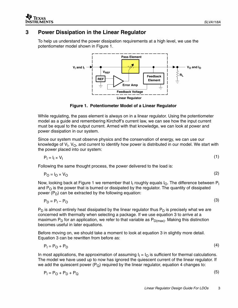
3 Power Dissipation in the Linear Regulator
To help us understand the power dissipation requirements at a high level, we use thepotentiometer model shown in Figure 1.
Pass Element
Error Amp
FeedbackElementREF
Feedback Voltage
RL
VI and II VO and IOVREF
Linear Regulator
Figure 1. Potentiometer Model of a Linear Regulator
While regulating, the pass element is always on in a linear regulator. Using the potentiometermodel as a guide and remembering Kirchoff’s current law, we can see how the input currentmust be equal to the output current. Armed with that knowledge, we can look at power andpower dissipation in our system.
Since our system must observe physics and the conservation of energy, we can use ourknowledge of VI, VO, and current to identify how power is distributed in our model. We start withthe power placed into our system:
PI = lI × VI
Following the same thought process, the power delivered to the load is:
PO = lO × VO
Now, looking back at Figure 1 we remember that II roughly equals IO. The difference between PIand PO is the power that is burned or dissipated by the regulator. The quantity of dissipatedpower (PD) can be extracted by the following equation:
PD = PI − PO
PD is almost entirely heat dissipated by the linear regulator thus PD is precisely what we areconcerned with thermally when selecting a package. If we use equation 3 to arrive at amaximum PD for an application, we refer to that variable as PD(max). Making this distinctionbecomes useful in later equations.
Before moving on, we should take a moment to look at equation 3 in slightly more detail.Equation 3 can be rewritten from before as:
PI = PO + PD
In most applications, the approximation of assuming II = IO is sufficient for thermal calculations.The model we have used up to now has ignored the quiescent current of the linear regulator. Ifwe add the quiescent power (PQ) required by the linear regulator, equation 4 changes to:
PI = PO + PD + PQ
(1)
(2)
(3)
(4)
(5)
SLVA118A
4 Linear Regulator Design Guide For LDOs
PQ is derived by multiplying the input voltage by the quiescent current of the regulator.Thermally, PQ is usually insignificant, as it is orders of magnitude smaller than the outputcurrent. For example, the TPS789xx series of 100 mA (or 0.1 A) low dropout regulators (LDO)has a typical IQ of 17 µA (or 0.000017 A). In an example where the TPS78925 is used with VI =3.3 V, VO = 2.5 V, and IO = 100 mA we can see how PQ (56 µW) is substantially smaller than PD(80 mW). Thus, out of practicality and for simplicity we examine the thermal considerations forlinear regulators based on equation 4 ignoring quiescent current.
Quiescent current can have a significant impact on efficiency in power sensitive applications.This is covered briefly in Other Useful Items (Chapter 8) and in more detail in the Efficiencyportion of TI application reports SLVA079 – Understanding the Terms and Definitions of Low-Dropout Voltage Regulators and SLVA072 – Technical Review of Low Dropout VoltageRegulator Operation and Performance, as listed in Appendix B.
Another topic that warrants a brief commentary is steady state verses transient or pulsed currentdemand of a load from its power supply. In many applications, an LDO supplies bothsteady-state and pulsed load current. A given design may have low duty cycle load transientcurrents in addition to the steady-state load. The current transients can approach the internalfixed current limit of the LDO, which is normally between 2 and 4 times the continuous currentrating of the device. However, if we have an excessive junction temperature rise, thermalshutdown is activated. The thermal shutdown junction temperature typically occurs at 150°C.Whether the thermal design is based upon the average load current or designed to handle themaximum peak current depends upon the duration and frequency of occurrence of the loadtransient. In either case we are safe if we do not exceed the absolute maximum junctiontemperature rating of the device.
Returning to PD, the power ratings of LDOs are normally based upon steady state operatingconditions. Steady-state conditions between junction and case are typically achieved in lessthan 10 seconds where several minutes may be required to achieve steady-state junction toambient. Transient thermal impedance illustrates the thermal response to a step change inpower. This information is provided for discrete power devices and normally not for integratedcircuits. The transient thermal response is a function of die size, die attach, and package. Welimit the scope of our discussion to steady-state thermal resistance.
By utilizing the thermal equations that follow in Chapter 4, we ensure that the junctiontemperature of our linear regulator remains within acceptable limits. A semiconductor’s longterm reliability is affected by its operating junction temperature; therefore, it is important tomaintain a junction temperature that falls below the manufacturers absolute maximum operatingjunction temperature. This restriction limits the device’s power dissipation capability. To do this,we need to calculate the maximum allowable dissipation, PD(max), and the actual dissipation, PD,which must be less than or equal to PD(max). How to make these calculations is what we explorenext.
Factors which influence thermal performance include PCB design, component placement,interaction with other components on the board, airflow, and altitude. There is no substitute for asystem level thermal analysis to ensure a successful design.
SLVA118A
5 Linear Regulator Design Guide For LDOs
4 Thermal Equations—Will My Part Work?
With an understanding of PD, now we can examine the thermal considerations PD generates.The following equation links PD to the thermal specifications for a linear regulator:
PD = (TJ − TA)/θJA
Where
θJA = theta ja (junction to ambient) − �C/W
TJ = junction temperature rating − �C
TA = ambient temperature − �C
PD = power dissipated in watts − W
Equation 6 enables us to relate power dissipation with the thermal characteristics of thedie/package combination and ambient temperature. It is useful to manipulate equation 6 to:
θJA = (TJ − TA)/PD
Equation 7 is useful as TJ, TA, and PD(max) (see equation 3) are often known quantities in anapplication. By using these three known values, equation 7 will tell us what value of θJA isnecessary in order to have enough thermal conductance or thermal dissipation capability for ourlinear regulator in a particular application. Having the appropriate thermal conductance ensuresthat the PD(max) does not exceed the PD that the linear regulator is capable of supporting.Exceeding the PD that the regulator can support creates extreme junction temperatures which inturn impact the reliability of the design. For the remainder of this application note, if we usePD(max) in equation 7 to determine a maximum θJA for an application, we are referring to it asθJA(max).
In looking at equation 7, θJA decreases with an increase in TA or PD. It follows that the lower θJAis from equation 7, the more challenging the thermal requirements. Additionally, the lower a θJAis specified in a data sheet, the better thermal conductance a device exhibits.
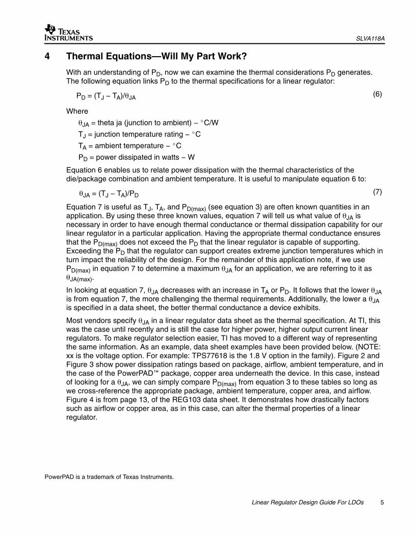
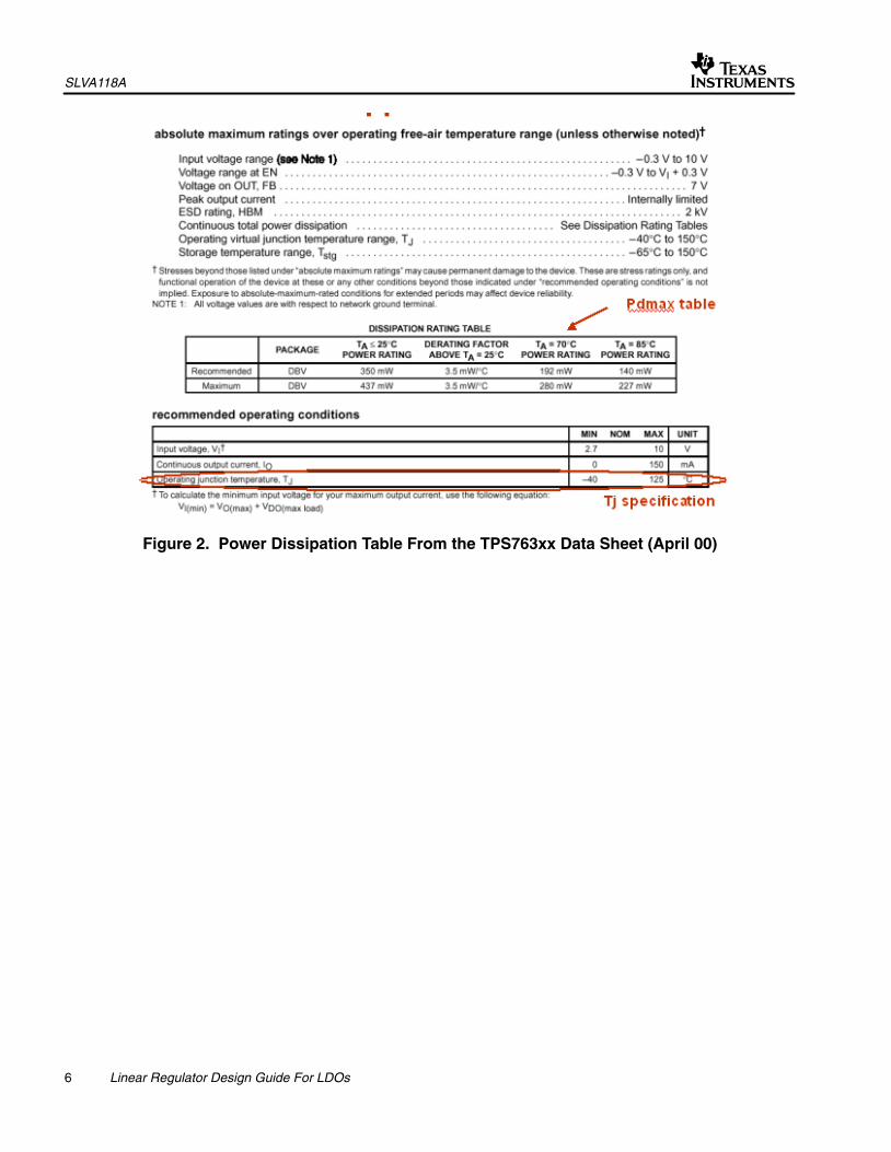
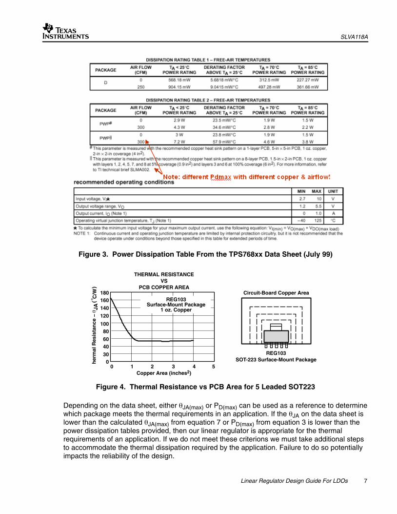
Most vendors specify θJA in a linear regulator data sheet as the thermal specification. At TI, thiswas the case until recently and is still the case for higher power, higher output current linearregulators. To make regulator selection easier, TI has moved to a different way of representingthe same information. As an example, data sheet examples have been provided below. (NOTE:xx is the voltage option. For example: TPS77618 is the 1.8 V option in the family). Figure 2 andFigure 3 show power dissipation ratings based on package, airflow, ambient temperature, and inthe case of the PowerPAD™ package, copper area underneath the device. In this case, insteadof looking for a θJA, we can simply compare PD(max) from equation 3 to these tables so long aswe cross-reference the appropriate package, ambient temperature, copper area, and airflow.Figure 4 is from page 13, of the REG103 data sheet. It demonstrates how drastically factorssuch as airflow or copper area, as in this case, can alter the thermal properties of a linearregulator.
PowerPAD is a trademark of Texas Instruments.
(6)
(7)
SLVA118A
6 Linear Regulator Design Guide For LDOs
Figure 2. Power Dissipation Table From the TPS763xx Data Sheet (April 00)
SLVA118A
7 Linear Regulator Design Guide For LDOs
Figure 3. Power Dissipation Table From the TPS768xx Data Sheet (July 99)
THERMAL RESISTANCEVS
PCB COPPER AREA180160
140
120
10080
6040
300
0 1 2 3 4 5Copper Area (inches2)
REG103Surface-Mount Package
1 oz. Copper
her
mal
Res
ista
nce
−JAθ
C/W
°()
Circuit-Board Copper Area
REG103SOT-223 Surface-Mount Package
Figure 4. Thermal Resistance vs PCB Area for 5 Leaded SOT223
Depending on the data sheet, either θJA(max) or PD(max) can be used as a reference to determinewhich package meets the thermal requirements in an application. If the θJA on the data sheet islower than the calculated θJA(max) from equation 7 or PD(max) from equation 3 is lower than thepower dissipation tables provided, then our linear regulator is appropriate for the thermalrequirements of an application. If we do not meet these criterions we must take additional stepsto accommodate the thermal dissipation required by the application. Failure to do so potentiallyimpacts the reliability of the design.
SLVA118A
8 Linear Regulator Design Guide For LDOs
5 Thermal Equations—What to Do if My Part Does not Work?
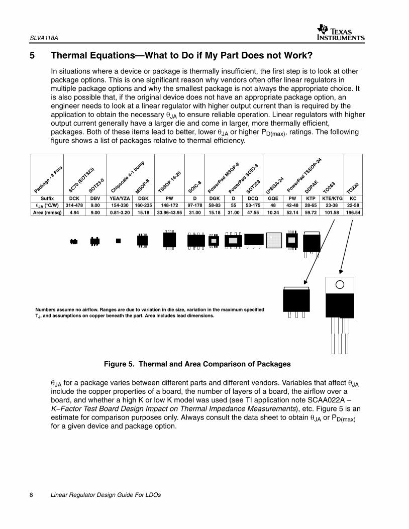
In situations where a device or package is thermally insufficient, the first step is to look at otherpackage options. This is one significant reason why vendors often offer linear regulators inmultiple package options and why the smallest package is not always the appropriate choice. Itis also possible that, if the original device does not have an appropriate package option, anengineer needs to look at a linear regulator with higher output current than is required by theapplication to obtain the necessary θJA to ensure reliable operation. Linear regulators with higheroutput current generally have a larger die and come in larger, more thermally efficient,packages. Both of these items lead to better, lower θJA or higher PD(max), ratings. The followingfigure shows a list of packages relative to thermal efficiency.
Area (mmsq) 4.94 9.00 0.81-3.20 15.18 33.96-43.95 31.00 15.18 31.00 47.55 10.24 52.14 59.72 101.58 196.54
θJA (°C/W) 314-478 9.00 154-330 160-235 148-172 97-178 58-83 55 53-175 48 42-48 28-65 23-38 22-58Suffix DCK DBV YEA/YZA DGK PW D DGK D DCQ GQE PW KTP KTE/KTG KC
Numbers assume no airflow. Ranges are due to variation in die size, variation in the maximum specifiedTJ, and assumptions on copper beneath the part. Area includes lead dimensions.
Figure 5. Thermal and Area Comparison of Packages
θJA for a package varies between different parts and different vendors. Variables that affect θJAinclude the copper properties of a board, the number of layers of a board, the airflow over aboard, and whether a high K or low K model was used (see TI application note SCAA022A –K−Factor Test Board Design Impact on Thermal Impedance Measurements), etc. Figure 5 is anestimate for comparison purposes only. Always consult the data sheet to obtain θJA or PD(max)for a given device and package option.
SLVA118A
9 Linear Regulator Design Guide For LDOs
There is some overlap and minor variation in packages depending on pin count and die size, butFigure 5 is a starting point for comparison of common packages. Also included in the list is TI’spatented PowerPAD™ packaging technology. PowerPAD footprints and dimensions remainstandard while the exposed thermal pad greatly enhances the thermal capabilities of thePowerPAD MSOP, TSSOP, and SOIC packages. For more information about PowerPAD, see TIapplication brief (http://www−s.ti/com/sc/techlit/slma004), PowerPAD Made Easy, and/orapplication note, (http://www−s.ti/com/sc/techlit/slma002), PowerPAD Thermally EnhancedPackage. Both of these documents are listed in Appendix B.
Where thermal considerations are challenging, another approach is to look at a switchingregulator. Often, the additional efficiency that can be possible with a switching design canalleviate thermal issues faced when using a linear regulator approach. There are manyconsiderations in migrating from a linear to a switching design that are beyond the scope of thisapplication report.
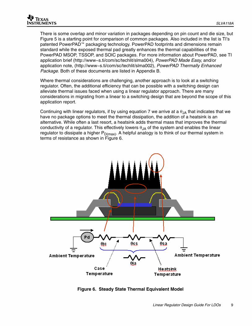
Continuing with linear regulators, if by using equation 7 we arrive at a θJA that indicates that wehave no package options to meet the thermal dissipation, the addition of a heatsink is analternative. While often a last resort, a heatsink adds thermal mass that improves the thermalconductivity of a regulator. This effectively lowers θJA of the system and enables the linearregulator to dissipate a higher PD(max). A helpful analogy is to think of our thermal system interms of resistance as shown in Figure 6.
Figure 6. Steady State Thermal Equivalent Model
SLVA118A
10 Linear Regulator Design Guide For LDOs
In this example, we are referring to:θJA = theta JA (junction to ambient) − °C/WθJC = theta JC (junction to case) − °C/WθCS = theta CS (case to heatsink) − °C/WθSA = theta SA (heatsink to ambient) − °C/W
NOTE: θCS is the thermal interface between the device case and the sink whether it is air,PCB/solder, or any other kind of heatsink.
Our simplified steady state heat transfer model is analogous to Ohm’s law. Power dissipation isanalogous to current, θ is analogous to electrical resistance, and ambient temperature isanalogous to ground potential or our reference point. We have used θJA up to now as we weredepending on the package for a complete thermal system from junction to ambient. Since aheatsink has been added, it is necessary to break the system down into more granularcomponents.
Adding a heatsink achieves a system θ junction to ambient low enough to meet the systemthermal requirements. A heatsink accomplishes this by offering a better thermal interface to airversus the package alone. Thus, we require the following to be met:
θJA(max) ≥ θJC + θCS + θSA
Where θJA(max) is the max acceptable thermal rating that meets the system requirements. Thisequation can be manipulated to:
θSA ≤ θJA(max) − θJC − θCS
If we refer back to equation 7, we can substitute (TJ – TA)/PD for θJA to obtain a θJA(max) andarrive at:
θSA ≤ [(TJ − TA)/PD(max)] − θJC − θCS
Equation 10 gives the designer one equation of what are normally known variables and yieldsthe maximum allowable value for a heatsink in an application.
The value of θCS depends upon the interface material and device mounting. In the case of aPowerPAD or a TO-263 package where the exposed pad is soldered directly to the bareprinted-circuit board copper, θCS is essentially 0°C/W. For a TO-220 package, which is mountedto a heatsink with a bolt or clip, a thermal interface material is used to fill voids between the taband heat sink. The interface thermal resistance depends upon the material used and is effectedby the mounting pressure, material thickness, and flatness of each surface. Typical values ofcommon interface material range between 0.1°C/W and 1°C/W and if no interface material isused could be as high as 5°C/W.
The user should consult the interface or heat sink vender to determine a suitable material tomeet the desired design goals.
By solving equation 10, we arrive at the required thermal impedance of the heatsink. Somepackages, such as the TO-220, TO-263, or DDPAK better lend themselves to using heatsinks.Packages such as the SC70 and SOT23 due to their physical size, are not generally consideredfor use with heatsinks. Appendix A has a short list of some thermal management vendors. Thevendors listed do offer various solutions for different package types. TI does not endorse onevendor over another and there are many other thermal management vendors not listed.
(8)
(9)
(10)
SLVA118A
11 Linear Regulator Design Guide For LDOs
Having read this far, the reader should have a basic understanding of the following:
• Why thermal considerations are important in linear regulator design
• Thermal equations for a linear regulator
• How to thermally evaluate different regulators for a design
The subsequent chapters of this applications report include a summary, real world examples,items to look out for, and appendixes including reference material, and additional usefulinformation on linear regulators and TI PowerPAD packaging technology.
SLVA118A
12 Linear Regulator Design Guide For LDOs
6 Summary of Approach and Equations
This chapter is a one page summary engineers can use to quickly evaluate a linear regulator.
With VI, VO, and IO (max) in hand, calculate PD(max) with:
PD(max) = PI − PO
= (VI − VO) × IO
NOTE: The IQ of the linear regulator is ignored due to its relative small size to IO. Thus, weassume lI = lO.
Then, take PD(max) and consult the data sheets of all perspective linear regulators. If the datasheet has power dissipation tables in watts, use PD(max) and compare the package with therating associated with the appropriate ambient temperature, copper area, and airflow. If the datasheet only offers a θJA for the package, calculate θJA(max) using:
θJA(max) = (TJ − TA)/PD(max)
If PD(max) is less than the power noted in the power dissipation table or θJA in the data sheet isless than the θJA(max) calculated in equation 7, the package is thermally acceptable. Otherwise,the package is not acceptable and an alternative should be found. Also, always be sure toreference θJA or PD(max) with the appropriate copper area and airflow for the application whenreading a data sheet.
In the case where the initial linear regulator is thermally insufficient, the easiest alternative is tolook for a different package. Figure 5 is a reasonable reference to help start such a search. It ispossible a linear regulator with more output current capability than required by the applicationmay be necessary to obtain the appropriate thermal properties.
If no package can be found to meet the thermal needs for the application, the next step is toconsider the addition of a heatsink or move to a switching power solution. When looking for aheatsink, use θJA calculated in equation 7 and substitute it into equation 9:
θSA ≤ θJA(max) − θJC − θCS
This yields the θSA required for the heatsink. The other major considerations in choosing aheatsink are form factor and mounting options for the linear regulator package.
(3)(11)
(7)
(9)
SLVA118A
13 Linear Regulator Design Guide For LDOs
7 Things Often OverlookedIncluded in this chapter are answers to common questions and items that are often overlooked.
7.1 Differences Between Vendors
In making a thermal comparison between linear regulator vendors, always check the data sheet.Different manufacturers are more or less aggressive in specifying θJA and the maximumrecommended junction temperature for a given package type. In addition, different vendorsmake different assumptions on things such as airflow or copper area under a device. Lead frameoptions such as TI’s PowerPAD can also drastically alter the thermal capabilities of a package.
Never assume similar parts have similar thermal capabilities, particularly when they come fromdifferent vendors, and always be aware of what assumptions or conditions the specificationsassume.
7.2 The Math Does Not Work... But the Part Does
It is not uncommon to find situations where the thermal equations indicate a potential problembut a part seems to work. Recall equation 7:
θJA = (TJ − TA)/PD
does not take into account airflow or the potential benefits of heatsinking into the PCB copper. Inaddition, manufacturers build headroom into their specifications. The cumulative headroom thisprovides could allow a part to work outside what is covered in the data sheet and this document.
If additional factors such as heatsinking into the PCB copper cannot account for why a partworks, it is not advised to continue to use it in a design. Violating the thermal ratings on a devicecan reduce the long-term reliability of the design.
The flip side to this is the situation where the original circuit was over-engineered for prototypingand exceeds what current the application requires. While the temptation is to leave the circuit asis, technically and financially it is often worth re-examining an over-engineered LDO. It can bepossible to obtain advantages in both cost and space with a minimal amount of work to populatethe function with a properly sized LDO.
7.3 Derating
Often, in demanding applications, companies have a policy of derating the integrated circuitsthey use. Depending on the project or end equipment this can be done in a variety of ways.From a thermal perspective, one often derates the absolute maximum junction temperature (TJ)for specific system reliability considerations when derating is necessary. This, in turn, decreasesθJA(max) in equation 6, which causes the application’s thermal design to be more demanding andoperation more robust.
It is up to the user to determine device suitability for a given application. It is important that thedevice operate within the manufacturers operating conditions stated in the data sheet. Deviceoperation at or above the absolute maximum ratings, which includes temperature, voltage, andcurrent causes premature device failure.
Several reliability prediction standards are used to assess product life such as MIL-HDBK-217Fand Bellcore TR-NWT-000332. Mil-HDBK-217F defines two prediction methods; a part stressanalysis and parts count reliability prediction.
(7)
SLVA118A
14 Linear Regulator Design Guide For LDOs
Common stresses that are known to accelerate device failure mechanisms include temperature,voltage, current, humidity, and temperature cycling. Temperature accelerates many chemical orphysical processes that may shorten the usable life of a semiconductor device.
The Arrhenius model is commonly used for semiconductor reliability prediction. The modelassumes that device failure rate is linear with time and that the acceleration factor is a functionof device junction temperature. The mean time between failure (MTBF) is defined as the inverseof the acceleration factor (f). Equation 12 shows the acceleration factor expressed as the ratio ofa time to fail at one temperature to a time to fail at a different temperature.
Acceleration factor f � t1t2
� exp �EaK� 1T1
� 1T2��
Where:Ea = Activation energy (ev)K = Boltzmans constant 8.6 x 10E−5 ev/°Kt1 = Time between failure at temperature T1t2 = Time between failure at temperature T2T1 = Junction temperature (°K) at time t1T2 = Junction temperature (°K) at time t2 where T2 >T1
We can use this equation to illustrate the effect on the MTBF by derating the maximumallowable junction temperature of the device. For this exercise we assume an activation energyof 0.9 ev. The manufacturers maximum operating junction temperature is found in the absolutemaximum ratings table in the data sheet. Many low dropout regulators are specified with anabsolute maximum rating of 125°C. If we reduce the maximum allowable junction temperatureby 10°C for a given design we see that the MTBF approximately doubles.
In many applications it is unnecessary to derate components. This discussion was provided asan example of one common way to derate components when necessary.
8 Other Useful Items
Included in this chapter are quick references to a few useful items regarding linear regulators.
8.1 Linear Regulator Efficiency
Efficiency of any power regulator is:
Eff = PO/PI × 100% = (VO × lO)/(VI × lI) × 100%
If we make the assumption as we did before that II = IO for a linear regulator discounting IQ dueto its relative size compared with IO, this can be simplified to:
Eff = VO/VI × 100%
This is a good rule of thumb, but remember, this only holds for a linear regulator design.Switching power supplies cannot be analyzed in this way.
There are applications that need to take into account the IQ of the linear regulator. To considerIQ, IO no longer equals II and thus equation 14 is invalid. To consider IQ, we examine equation 5:
(12)
(13)
(14)
SLVA118A
15 Linear Regulator Design Guide For LDOs
PI = PO + PD + PQ
Since quiescent power dissipation, PQ, is also derived from the input voltage, equation 13 canbe manipulated to:
Eff = (VO × lO)/[(VI × lI) + (VI × lQ)] × 100%
Assuming IQ comes from the same source, VI, as does II. An example where this is not the caseis the UC382 as it has a bias supply input, VB, which draws IQ. The UC382 aside and assumingboth II and IQ come from the same source, we return to our potentiometer module from Chapter3, and we conclude that:
Eff = (VO × lO)/[VI × (lO + lQ)] × 100%
Again, remember these equations only apply to a linear regulator design. One example of anapplication where this granularity could be important is in portable end equipments where theload is asleep for the majority of the time. With a very small load current for a significant amountof time, IQ can become a significant factor in efficiency and product run time. This is whycompanies such as TI have low IQ families of linear regulators. For comparison, the TPS761xxfamily of LDO’s has a typical quiescent current of 2.6 mA where the TPS769xx family has atypical quiescent current of 0.017 mA. Both are 100-mA LDOs, but the TPS769xx was designedfor power sensitive applications as are other TI LDOs which offer even lower IQ than theTPS769xx.
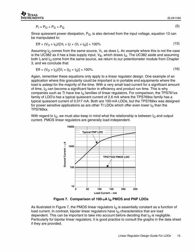
With regard to IQ, we must also keep in mind what the relationship is between IQ and outputcurrent. PMOS linear regulators are generally load independent.
Typical PNP LDO
TPS77333 PMOS LDO
100
100 50 100 150
Gro
un
d C
urr
ent
− 1000
Load Current − mA
10000
200 250
Aµ
Figure 7. Comparison of 100-�A lQ PMOS and PNP LDOs
As illustrated in Figure 7, the PMOS linear regulators IQ is essentially constant as a function ofload current. In contrast, bipolar linear regulators have IQ characteristics that are loaddependent. This can be important to take into account before deciding that IQ is negligible.Particularly for bipolar linear regulators, it is good practice to consult the graphs in the data sheetif they are provided.
(5)
(15)
(16)
SLVA118A
16 Linear Regulator Design Guide For LDOs
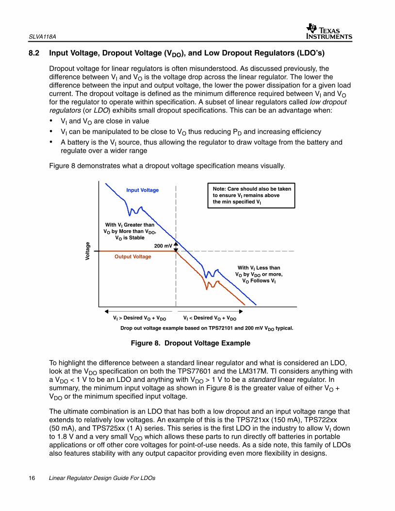
8.2 Input Voltage, Dropout Voltage (VDO), and Low Dropout Regulators (LDO’s)
Dropout voltage for linear regulators is often misunderstood. As discussed previously, thedifference between VI and VO is the voltage drop across the linear regulator. The lower thedifference between the input and output voltage, the lower the power dissipation for a given loadcurrent. The dropout voltage is defined as the minimum difference required between VI and VOfor the regulator to operate within specification. A subset of linear regulators called low dropoutregulators (or LDO) exhibits small dropout specifications. This can be an advantage when:
• VI and VO are close in value
• VI can be manipulated to be close to VO thus reducing PD and increasing efficiency
• A battery is the VI source, thus allowing the regulator to draw voltage from the battery andregulate over a wider range
Figure 8 demonstrates what a dropout voltage specification means visually.
Output Voltage
Input Voltage
With VI Greater thanVO by More than VDO,
VO is Stable
200 mV
With VI Less thanVO by VDO or more,
VO Follows VI
VI > Desired VO + VDO VI < Desired VO + VDO
Drop out voltage example based on TPS72101 and 200 mV VDO typical.
Vo
ltag
e
Note: Care should also be takento ensure VI remains abovethe min specified VI
Figure 8. Dropout Voltage Example
To highlight the difference between a standard linear regulator and what is considered an LDO,look at the VDO specification on both the TPS77601 and the LM317M. TI considers anything witha VDO < 1 V to be an LDO and anything with VDO > 1 V to be a standard linear regulator. Insummary, the minimum input voltage as shown in Figure 8 is the greater value of either VO +VDO or the minimum specified input voltage.
The ultimate combination is an LDO that has both a low dropout and an input voltage range thatextends to relatively low voltages. An example of this is the TPS721xx (150 mA), TPS722xx(50 mA), and TPS725xx (1 A) series. This series is the first LDO in the industry to allow VI downto 1.8 V and a very small VDO which allows these parts to run directly off batteries in portableapplications or off other core voltages for point-of-use needs. As a side note, this family of LDOsalso features stability with any output capacitor providing even more flexibility in designs.
SLVA118A
17 Linear Regulator Design Guide For LDOs
9 Real World Examples
Included in this chapter are four real world examples to further illustrate the thermal conceptspresented in this application report.
Example 1:
We need to power a C5409 DSP core with a small amount of additional logic at 1.8 V. Theapplication calls for a 100 mA solution at 1.8 V and this rail needs to be created from 5 V. Themaximum ambient temperature is 70°C, and we assume zero airflow. The TPS76318 andREG101-A linear regulators are under consideration. Which device(s) and package options areacceptable?
Answer:
As a side note, if we take a quick look at efficiency with equation 14:
Eff = VO/VI × 100%Eff = 1.8 V/5 V × 100% = ~36%
Obviously, a linear regulator is not the optimal solution for efficiency in this case but we assumeefficiency is not a primary design goal in this application.
Both the TPS76318 and REG101-A have an acceptable input voltage range, output voltagerange, and output current capability. The potential pitfall in this application are the thermalconsiderations.
Ignoring the IQ of the linear regulator, at 100 mA output current we calculate the input and outputpower:
Output Power: P = I × V = 100 mA × 1.8 V = 180 mWInput Power: P = I × V = 100 mA × 5 V = 500 mW
PD = PI – POPD(max) = 500 mW – 180 mW = 320 mW
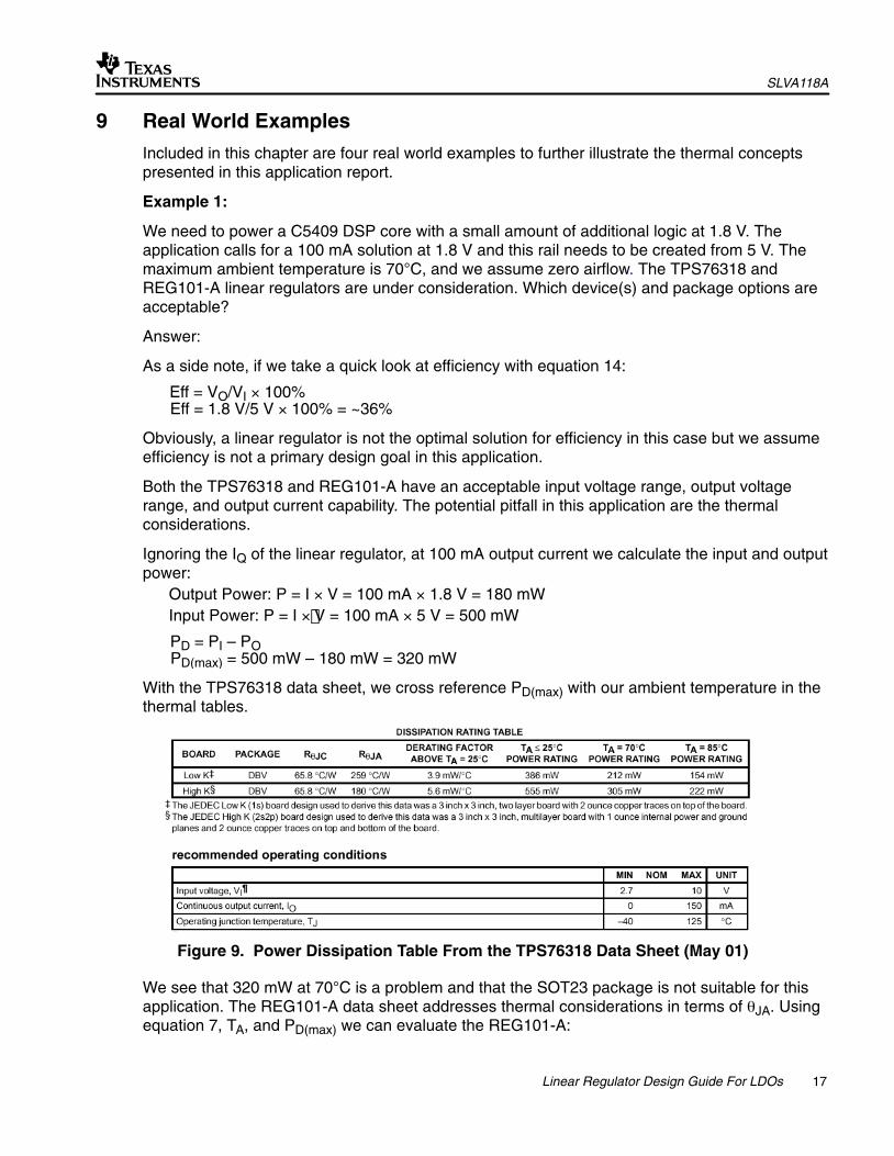
With the TPS76318 data sheet, we cross reference PD(max) with our ambient temperature in thethermal tables.
Figure 9. Power Dissipation Table From the TPS76318 Data Sheet (May 01)
We see that 320 mW at 70°C is a problem and that the SOT23 package is not suitable for thisapplication. The REG101-A data sheet addresses thermal considerations in terms of θJA. Usingequation 7, TA, and PD(max) we can evaluate the REG101-A:
SLVA118A
18 Linear Regulator Design Guide For LDOs
θJA = (TJ – TA)/PDθJA = (125°C – 70°C)/0.320 W = ~171°C/W
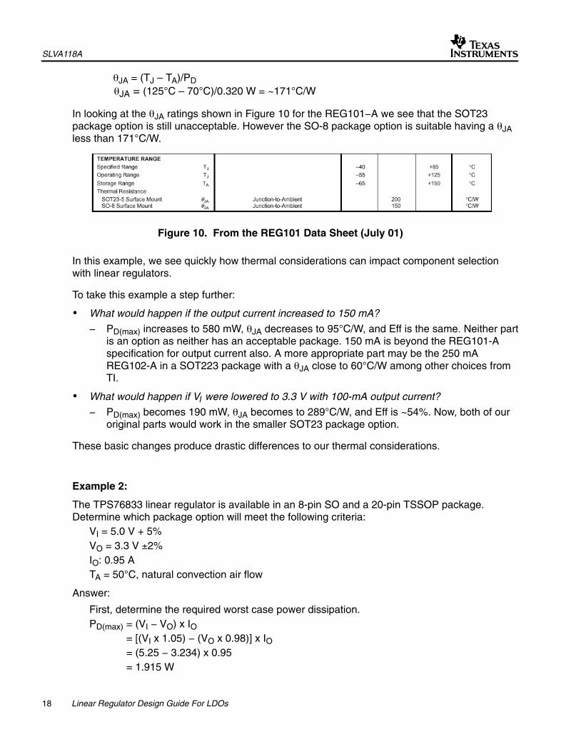
In looking at the θJA ratings shown in Figure 10 for the REG101−A we see that the SOT23package option is still unacceptable. However the SO-8 package option is suitable having a θJAless than 171°C/W.
Figure 10. From the REG101 Data Sheet (July 01)
In this example, we see quickly how thermal considerations can impact component selectionwith linear regulators.
To take this example a step further:
• What would happen if the output current increased to 150 mA?
− PD(max) increases to 580 mW, θJA decreases to 95°C/W, and Eff is the same. Neither partis an option as neither has an acceptable package. 150 mA is beyond the REG101-Aspecification for output current also. A more appropriate part may be the 250 mAREG102-A in a SOT223 package with a θJA close to 60°C/W among other choices fromTI.
• What would happen if VI were lowered to 3.3 V with 100-mA output current?
− PD(max) becomes 190 mW, θJA becomes to 289°C/W, and Eff is ~54%. Now, both of ouroriginal parts would work in the smaller SOT23 package option.
These basic changes produce drastic differences to our thermal considerations.
Example 2:
The TPS76833 linear regulator is available in an 8-pin SO and a 20-pin TSSOP package.Determine which package option will meet the following criteria:
VI = 5.0 V + 5%VO = 3.3 V ±2%IO: 0.95 ATA = 50°C, natural convection air flow
Answer:
First, determine the required worst case power dissipation.PD(max) = (VI − VO) x IO
= [(VI x 1.05) − (VO x 0.98)] x IO = (5.25 − 3.234) x 0.95 = 1.915 W
SLVA118A
19 Linear Regulator Design Guide For LDOs
Now determine the maximum package thermal impedance requirement given the above criteria.PD(max) = (TJ(max) − TA)/θJA Rearranging and solving for θJA
θJA ≤ (TJ(max) − TA)/PD(max)
From the TPS76815 data sheet we see that the absolute maximum junction temperature is125°C. In this application, your company mandates that all components have derated TJ(max).For this example we derate by 10°C.
Let TJ(max) = 115°C
Therefore the required θJA ≤ (115 – 50)°C/1.915 W = 33.9°C/W
From the data sheet we see that the 8-pin SOIC package (D) does not meet the requirementsince it has a θJA of 172°C/W. The 20-pin TSSOP PowerPAD package (PWP) meets therequirement having a θJA of 32.6°C/W if it is mounted on a board having a copper heat sink areaof at least four square inches (1 oz. copper).
Example 3:
The REG104 linear regulator is available in a SOT223 and TO-263 surface mount packaging.Determine which package option meets the following criteria:
VI = 5.0 V + 5%
VO = 2.5 V ±2%IO: 1.0 A
TA = 50°C, natural convection air flow
Answer:
First, determine the required worst case power dissipation:PD(max) = (VI − VO) x IO
= [(VI x 1.05) − (VO x 0.98)] x IO = (5.25 − 2.45) x 1 = 2.8 W
Now determine the maximum package thermal impedance requirement given the above criteria.
PD(max) = (TJ(max) − TA)/θJA Rearrange and solving for θJA
θJA ≤ (TJ(max) − TA)/PD(max)
From the REG104 data sheet we see that the absolute maximum junction temperature is 150°C.Thus,
Let TJ(max) = 150°C
Therefore the required θJA ≤ (150 – 50)°C/2.8 W = 35.7°C/W
From Figure 10 of the REG104 data sheet we see that a TO-263 mounted on 1.5 square inchesof 1 oz. copper has a θJA of 32°C/W. Since the mounting tab is at ground potential, the entireground plane can be used to further reduce the thermal impedance.
SLVA118A
20 Linear Regulator Design Guide For LDOs
Example 4:Given that a TMS320C6201 DSP has the following system requirements:
Core: 1.8 V ±3% at 1.0 WI/O: 3.3 V ±5% at 0.2 WVI = 5.0 V ±5%TA = 50°C
Find a suitable power solution using a dual LDO regulator to power the DSP system.
We must first determine the total power dissipation required for the dual regulator.PD(core) = (VI − Vcore)) x I(core)
= (VI(1.05) – Vcore(0.97)) Pcore/Vcore(0.97)= (5.25 – 1.75) (1.0)/1.75 = 2.0 W
PD(I/O) = (VI − VO(I/O)) x I(I/O)
= (VI(1.05) – VI/O(0.95)) PI/O/VI/O(0.95)= (5.25 – 3.14) (0.2)/3.14 = 0.134 W
Total regulator dissipation = PD(core) + PD(I/O) = 2.0 W + 0.124 W = 2.124 W
Next, determine the required maximum package thermal impedance.
Maximum allowable dissipation:
PD(max) = (TJ(max) − TA)/θJA
θJA ≤ (TJ(max) − TA)/PD(max)
Most of the TI LDO data sheets list an absolute maximum junction temperature rating of 125°C.Thus,
Let TJ(max) = 125°C
Therefore θJA ≤ (125 – 50)/2.124 = 35.3°C
The DSP power selection matrix table (page 35) of the Power Management Selection Guide,literature number SLVT145 recommends the TPS767D318 as a possible product to meet thesystem requirements. From the TPS767D318 data sheet we find that it meets the voltage andtolerance requirements as well as thermal. It features a θJA of 32.6°C/W if at least four squareinches of 1 oz. copper heat sink area is used. Since the thermal pad is at ground potential, theentire ground plane could be used to further reduce the thermal impedance.
SLVA118
21 Digital Designer’s Guide to Linear Voltage Regulators and Thermal Management
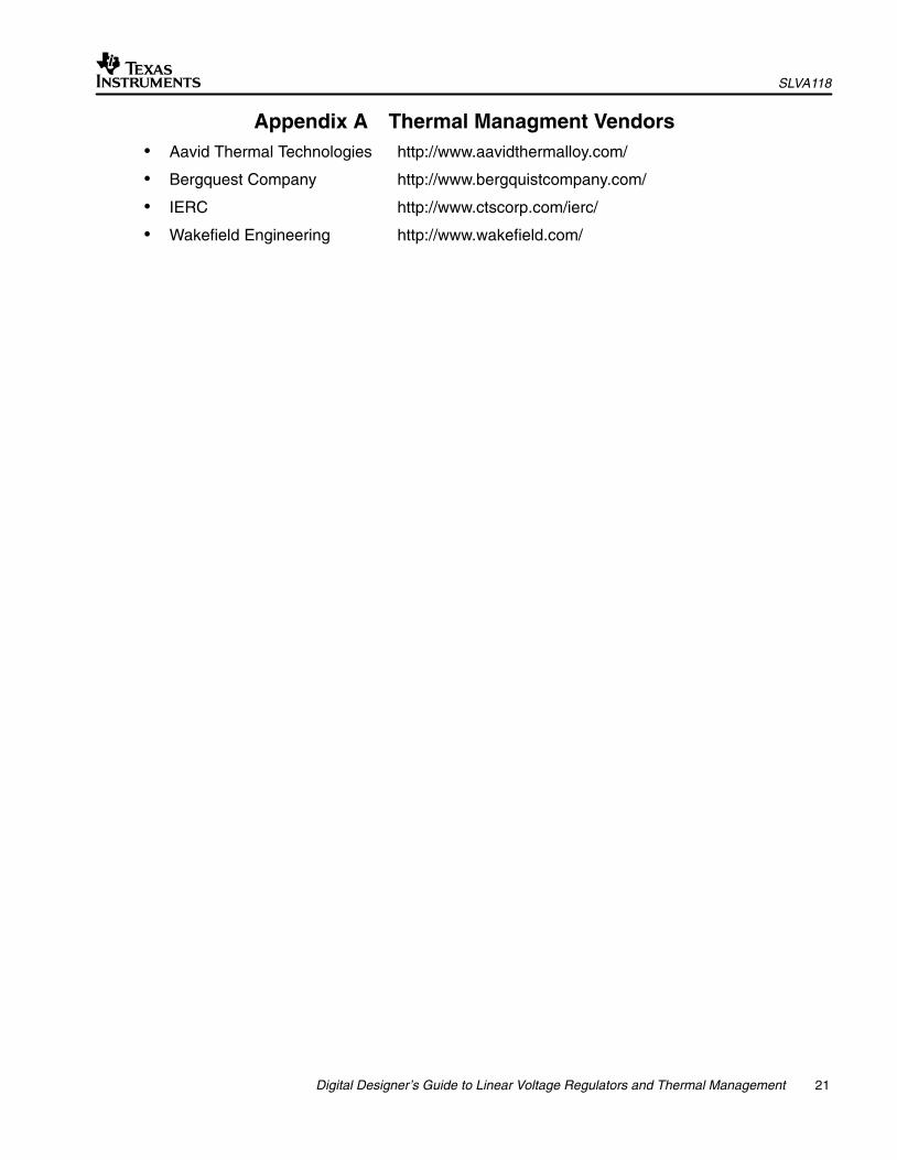
Appendix A Thermal Managment Vendors• Aavid Thermal Technologies http://www.aavidthermalloy.com/
• Bergquest Company http://www.bergquistcompany.com/
• IERC http://www.ctscorp.com/ierc/
• Wakefield Engineering http://www.wakefield.com/
SLVA118
22 Digital Designer’s Guide to Linear Voltage Regulators and Thermal Management
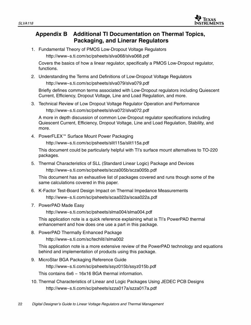
Appendix B Additional TI Documentation on Thermal Topics, Packaging, and Linerar Regulators
1. Fundamental Theory of PMOS Low-Dropout Voltage Regulators
http://www−s.ti.com/sc/psheets/slva068/slva068.pdf
Covers the basics of how a linear regulator, specifically a PMOS Low-Dropout regulator,functions.
2. Understanding the Terms and Definitions of Low-Dropout Voltage Regulators
http://www−s.ti.com/sc/psheets/slva079/slva079.pdf
Briefly defines common terms associated with Low-Dropout regulators including QuiescentCurrent, Efficiency, Dropout Voltage, Line and Load Regulation, and more.
3. Technical Review of Low Dropout Voltage Regulator Operation and Performance
http://www−s.ti.com/sc/psheets/slva072/slva072.pdf
A more in depth discussion of common Low-Dropout regulator specifications includingQuiescent Current, Efficiency, Dropout Voltage, Line and Load Regulation, Stability, andmore.
4. PowerFLEX™ Surface Mount Power Packaging
http://www−s.ti.com/sc/psheets/slit115a/slit115a.pdf
This document could be particularly helpful with TI’s surface mount alternatives to TO-220packages.
5. Thermal Characteristics of SLL (Standard Linear Logic) Package and Devices
http://www−s.ti.com/sc/psheets/scza005b/scza005b.pdf
This document has an exhaustive list of packages covered and runs though some of thesame calculations covered in this paper.
6. K-Factor Test-Board Design Impact on Thermal Impedance Measurements
http://www−s.ti.com/sc/psheets/scaa022a/scaa022a.pdf
7. PowerPAD Made Easy
http://www−s.ti.com/sc/psheets/slma004/slma004.pdf
This application note is a quick reference explaining what is TI’s PowerPAD thermalenhancement and how does one use a part in this package.
8. PowerPAD Thermally Enhanced Package
http://www−s.ti.com/sc/techlit//slma002
This application note is a more extensive review of the PowerPAD technology and equationsbehind and implementation of products using this package.
9. MicroStar BGA Packaging Reference Guide
http://www−s.ti.com/sc/psheets/ssyz015b/ssyz015b.pdf
This contains 6x6 − 16x16 BGA thermal information.
10. Thermal Characteristics of Linear and Logic Packages Using JEDEC PCB Designs
http://www−s.ti.com/sc/psheets/szza017a/szza017a.pdf
SLVA118
23 Digital Designer’s Guide to Linear Voltage Regulators and Thermal Management
11. Thermal Derating Curves for Logic-Products Packages
http://www−s.ti.com/sc/psheets/szza013a/szza013a.pdf
12. PT3100/4100 Series Application note revised 5/15/98.
13. TI external website for packaging information
http://www.ti.com/sc/docs/package/pkg_thermal_db.htm
As an example, if looking for TSSOP information: Enter packaging group = all, package typeTSSOP, JEDEC design guidelines = all, Then SEARCH.
NOTE: urls are provided for quick reference, but as the web is always changing please beaware that these links may change as well! If you have trouble finding one of these documents,please contact your local TI representative or your regional TI Product Information Center.
SLVA118
24 Digital Designer’s Guide to Linear Voltage Regulators and Thermal Management
Appendix C Other References1. S. M. Sze, VLSI Technology, McGraw-Hill, New York, 1988.
2. AN1029 Fairchild, April, 1996Maximum Power Enhancement Techniques for SO-8 Power MOSFETsAlan Li, Brij Mohan, Steve Sapp, Izak Bencuya, Linh HongNote: Related documents include AN1028, AN1025, AN1026 for other packages.
3. AN−569, Motorola, 1973Transient Thermal Resistance—General Data and Its UseBill Roehr and Bryce Shiner
IMPORTANT NOTICE
Texas Instruments Incorporated and its subsidiaries (TI) reserve the right to make corrections, enhancements, improvements and otherchanges to its semiconductor products and services per JESD46C and to discontinue any product or service per JESD48B. Buyers shouldobtain the latest relevant information before placing orders and should verify that such information is current and complete. Allsemiconductor products (also referred to herein as “components”) are sold subject to TI’s terms and conditions of sale supplied at the timeof order acknowledgment.
TI warrants performance of its components to the specifications applicable at the time of sale, in accordance with the warranty in TI’s termsand conditions of sale of semiconductor products. Testing and other quality control techniques are used to the extent TI deems necessaryto support this warranty. Except where mandated by applicable law, testing of all parameters of each component is not necessarilyperformed.
TI assumes no liability for applications assistance or the design of Buyers’ products. Buyers are responsible for their products andapplications using TI components. To minimize the risks associated with Buyers’ products and applications, Buyers should provideadequate design and operating safeguards.
TI does not warrant or represent that any license, either express or implied, is granted under any patent right, copyright, mask work right, orother intellectual property right relating to any combination, machine, or process in which TI components or services are used. Informationpublished by TI regarding third-party products or services does not constitute a license to use such products or services or a warranty orendorsement thereof. Use of such information may require a license from a third party under the patents or other intellectual property of thethird party, or a license from TI under the patents or other intellectual property of TI.
Reproduction of significant portions of TI information in TI data books or data sheets is permissible only if reproduction is without alterationand is accompanied by all associated warranties, conditions, limitations, and notices. TI is not responsible or liable for such altereddocumentation. Information of third parties may be subject to additional restrictions.
Resale of TI components or services with statements different from or beyond the parameters stated by TI for that component or servicevoids all express and any implied warranties for the associated TI component or service and is an unfair and deceptive business practice.TI is not responsible or liable for any such statements.
Buyer acknowledges and agrees that it is solely responsible for compliance with all legal, regulatory and safety-related requirementsconcerning its products, and any use of TI components in its applications, notwithstanding any applications-related information or supportthat may be provided by TI. Buyer represents and agrees that it has all the necessary expertise to create and implement safeguards whichanticipate dangerous consequences of failures, monitor failures and their consequences, lessen the likelihood of failures that might causeharm and take appropriate remedial actions. Buyer will fully indemnify TI and its representatives against any damages arising out of the useof any TI components in safety-critical applications.
In some cases, TI components may be promoted specifically to facilitate safety-related applications. With such components, TI’s goal is tohelp enable customers to design and create their own end-product solutions that meet applicable functional safety standards andrequirements. Nonetheless, such components are subject to these terms.
No TI components are authorized for use in FDA Class III (or similar life-critical medical equipment) unless authorized officers of the partieshave executed a special agreement specifically governing such use.
Only those TI components which TI has specifically designated as military grade or “enhanced plastic” are designed and intended for use inmilitary/aerospace applications or environments. Buyer acknowledges and agrees that any military or aerospace use of TI componentswhich have not been so designated is solely at the Buyer's risk, and that Buyer is solely responsible for compliance with all legal andregulatory requirements in connection with such use.
TI has specifically designated certain components which meet ISO/TS16949 requirements, mainly for automotive use. Components whichhave not been so designated are neither designed nor intended for automotive use; and TI will not be responsible for any failure of suchcomponents to meet such requirements.
Products Applications
Audio www.ti.com/audio Automotive and Transportation www.ti.com/automotive
Amplifiers amplifier.ti.com Communications and Telecom www.ti.com/communications
Data Converters dataconverter.ti.com Computers and Peripherals www.ti.com/computers
DLP® Products www.dlp.com Consumer Electronics www.ti.com/consumer-apps
DSP dsp.ti.com Energy and Lighting www.ti.com/energy
Clocks and Timers www.ti.com/clocks Industrial www.ti.com/industrial
Interface interface.ti.com Medical www.ti.com/medical
Logic logic.ti.com Security www.ti.com/security
Power Mgmt power.ti.com Space, Avionics and Defense www.ti.com/space-avionics-defense
Microcontrollers microcontroller.ti.com Video and Imaging www.ti.com/video
RFID www.ti-rfid.com
OMAP Mobile Processors www.ti.com/omap TI E2E Community e2e.ti.com
Wireless Connectivity www.ti.com/wirelessconnectivity
Mailing Address: Texas Instruments, Post Office Box 655303, Dallas, Texas 75265Copyright © 2012, Texas Instruments Incorporated