digital design review - oregon state...
TRANSCRIPT

Digital Design Review
I Why?I You never learned how - traffic light controllersI You have forgotten or are rustyI You have bad habits (ad hoc, asynchronous design, old technology)I You need a method that will work for more complex designs
I We will learn on simple designs, then add complexity

Digital Design Review
I Why not jump into System Verilog (SV) now?I If you can’t correctly do digital design, SV only helps you make
mistakes more quickly!I SV describes circuits, it dosen’t design circuits. (coding 6=design)I SV 6= design tool. Block, timing and state machine diagrams are.I Typically, coding begins once the design is finished.I We use SV templates to implement our designs. Writing SV code
should be a nearly mindless translation step.I Clever code 6= clever circuit design. ”Optimizing” SV code is useless
in the conventional sense except for simulation. Synthesis probablyignores your clever code anyway!
I Good designs stem from good architecture (structure), not clevercode.
A problem occurs when we think that using System Verilog is all about”coding up” designs. Coding is not the emphasis. Instead, the focus is ondescribing an already defined hardware structure. The design process isnot ”coding”. Design is a separate, earlier step, done with different tools.

Digital Design Review
I C and System Verilog are very different animalsI C compilation is a translation from complex instructions to simple in
a model that is inherrently sequential with a single thread of control.
for(i=0;i<=5;i++){ numb ++}
becomes
mov i, 5;
loop: inc numb;
dec i;
jnz lp;
I System Verilog compilation is very differentI Logic synthesis infers or deduces from code structure a gate-level
logic structure from the abstract description of circuit behavior givenby a language that models parallel operation.

Digital Design Review: 32x32 Multiplier
I Longhand multiplication
11101001x
1110 0000 0000 1110
1111110
I Check first (LSB) bit of multiplier, if multiplier is a one, save a copyof multiplicand, else save all zeros.
I Check next bit of multiplier, if its a one, left-shift the multiplicandonce and add it to the previously saved value. Else, add only zeros.
I Once all bits of the multiplicand are checked, and additionsperformed, the sum is the product.

Digital Design Review: 32x32 Multiplier
I Design constraints:I Synchronous (not combinatorial) using edge-triggered flip-flopsI One clock, rising edge only, never gatedI One reset, asynchronous, applied at power-upI One input to tell us to start, one output to indicate completion
I Now, ask, ”what structures and paths do I need to implement themultiplication?”
I Need storage for operands and product plus an adderI These will be flip-flops, not RAM. RAM makes no sense and is very
expensive.I Then, what data paths will be needed between the blocks?
Digital Design Review: 32x32 Multiplier
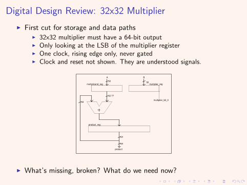
I First cut for storage and data pathsI 32x32 multiplier must have a 64-bit outputI Only looking at the LSB of the multiplier registerI One clock, rising edge only, never gatedI Clock and reset not shown. They are understood signals.
FILE: REVISION:
DRAWN BY: PAGE OF
TITLE
multiplier_regmultiplicand_reg
product_reg
3232
multiplier_bit_0
A B
64
64
64
32 ??
product
I What’s missing, broken? What do we need now?

Digital Design Review: 32x32 Multiplier
I Clean up initial design - fix data paths, add some control stubsI Need 64-bit multiplicand register to shift left up-to 32 timesI Need to be able to load the operand registersI Need to be able to load or hold value in product (free running clock)
FILE: REVISION:
DRAWN BY: PAGE OF
TITLE
multiplier_regmultiplicand_reg
product_reg
3232
multiplier_bit_0
A B
shift_left
64
64
shift_right
load_prod_reg
64
64
load_operands
product

Digital Design Review: 32x32 Multiplier
I Add remaining control signalsI Upper 32 bits of multiplicand, product register needs to be clearedI Add ”start” and ”done” signals
FILE: REVISION:
DRAWN BY: PAGE OF
TITLE
multiplier_regmultiplicand_reg
product_reg
3232
mult_control
multiplier_bit_0
A B
shift_left
64
64
shift_right
load_prod_reg
whole register isinitalized to zeroat beginning64
64
load_operands
start_mult
clear_regs
upper half isinitalized to zeroat beginning
I High-level block diagram is done! Time for a noggin simulation.
I Control is abstracted away into its own block.

Digital Design Review: 32x32 Multiplier
I By now, you should see some optimizations that can be made.
I Approaching the design as we have exposes optimizations clearly.
I A ”code first” approach will not reveal these optimizations.
I ”Optimizing” your HDL code will never create theseoptimizations, as they are based in the structure of the hardware.
I ”Optimizing” HDL code very often gives you exactly the samestructure, only with more difficult to read code.

Digital Design Review: 32x32 Multiplier
I First OptimizationI The multiplicand register is filled with zeros as its shifted left. Half of
it only holds zeros that the 64-bit ALU had to process.I Consider: don’t shift the multiplicand but shift the product right.I Result: 32-bit multiplicand register and ALU. No synchronous reset
required for the product or multiplicand register.
FILE: REVISION:
DRAWN BY: PAGE OF
TITLE
multiplier_regmultiplicand_reg
product_reg
3232
mult_control
multiplier_bit_0
A B
32shift_right
load_prod_reg
64
32
load_operands
start_mult
32
shift_right
32 32

Digital Design Review: 32x32 Multiplier
I Final OptimizationI Any values in the lower half of the product register are discarded as it
is shifted right. The wasted space is exactly the size of the multiplier.I As wasted space in the product disappears, so does the multiplier.I Lower half of the product register temporarily stores multiplier.I Result: Removal of the 32-bit multiplier register and simpler control.
FILE: REVISION:
DRAWN BY: PAGE OF
TITLE
multiplicand_reg
product_reg
32
32
mult_control
multiplier_bit_0
A B
32
shift_right
load_prod_reg
64
32
load_operands
start_mult
32
32 32
32

Digital Design Review: 32x32 Multiplier
I With an acceptable architecture we can create the control signalsand tidy things up a bit. Fortunately, we have a simpler datapath tocontrol.
FILE: REVISION:
DRAWN BY: PAGE OF
TITLE
multiplicand_reg
prod_reg_high
32
32
mult3_ctl
multiplier_bit_0
a_in b_in
32
shift
load
64
32
start
32
32 32
32
done
shift
load
prod_reg_shift_rt
reg_a
’0
0 1S start
start
startB
LS
product
prod_reg_ld_high
prod_reg_low
D
Q
D
Q
D
Q

Digital Design Review: 32x32 Multiplier
I Ground-rules for our control designI All control signals are synchronous to one clock (rising edge)I All control signals are created in synchronous state machines.I All control signals change state at rising clock edge.I All data movement happens at the rising clock edges.I Clock is never gated, we use enabled flip-flops.
I Use timing diagram and state machine diagrams to develop
I Start with either, go back and forth making sure they agree and thatthe signals are created at the correct time.

Digital Design Review: 32x32 Multiplier
I Why timing and state machine diagrams?
I Algorithms describe what things happen in a sequential manner.Parallelism is hidden.
I Timing Diagrams describe when things happen in a parallel manner.Parallelism is exposed.
I State Machine Diagrams separate parallel operations into easier tounderstand mini-machines.
I The visual nature of timing and state machines allow the use ofvisual pattern matching to observe commonality, see mistakes andto simplify our designs.

Digital Design Review: 32x32 MultiplierI Timing and state machine diagrams are best worked out with paper
and pencil or whiteboards.I Producing these diagrams is another eraser-intensive exercise. Its
hard work, and worth every minute.I Time spent here is equal to 5x-10x time debugging HDL code.
I We will finish the timing and state diagrams as a homeworkassignment.