digital design and test automation flow lab introduction...
TRANSCRIPT

KIT – University of the State of Baden-Wuerttemberg and National Research Center of the Helmholtz Association
INSTITUTE OF COMPUTER ENGINEERING (ITEC) – CHAIR FOR DEPENDABLE NANO COMPUTING (CDNC)
www.kit.edu
Digital Design and Test Automation Flow Lab
Introduction and Overview
Mehdi Tahoori
Chair of Dependable Nano-Computing, Faculty of Informatics2
Objective
Electronic Design Automation (EDA) Behind all novel electronic systems that we use in our daily lives
Such as iPod, smartphones, laptops, TVs, digital cameras, etc.
The objective of this lab To have a hands-on practice on major steps in digital design and test automation flow
From system-level specification to physical design and verification
Using industrial EDA toolsets
You will work on sample designs and go through all major design and test steps
Become familiar with the steps and tool chain in the digital design and test automation flow
Prof. Mehdi Tahoori
Chair of Dependable Nano-Computing, Faculty of Informatics3
Topics
System-level specification and simulation
High-level synthesis
Logic-level synthesis and simulation
Design for testability
Test pattern generation and fault simulation
Circuit design, simulation and verification
Timing analysis and closure
Area, delay, and power estimation and analysis
With a flavor of dependable computing
Prof. Mehdi Tahoori
Chair of Dependable Nano-Computing, Faculty of Informatics4
Structure
Block 1: System level design
Block 2: RTL design and test
Block 3: Circuit level design
Prof. Mehdi Tahoori

Chair of Dependable Nano-Computing, Faculty of Informatics5
VLSI Realization Process
Prof. Mehdi Tahoori
Determine requirements
specifications
Design synthesis and Verification
FabricationManufacturing test
Chips to customer
Customer’s need
Test development
Chair of Dependable Nano-Computing, Faculty of Informatics6
Definitions
Design synthesis: Given an Input-Output function, develop a procedure to manufacture a device using known materials and processes
Verification: Predictive analysis to ensure that the synthesized design, when manufactured, will perform the given Input-Output function
Prof. Mehdi Tahoori

Chair of Dependable Nano-Computing, Faculty of Informatics7
Y Chart
Prof. Mehdi Tahoori
Chair of Dependable Nano-Computing, Faculty of Informatics8
Y transformations
Prof. Mehdi Tahoori

Chair of Dependable Nano-Computing, Faculty of Informatics9
Design Steps
Prof. Mehdi Tahoori
Specifications High-levelDescriptionHigh-levelDescription
FunctionalDescriptionFunctionalDescription
BehavioralVHDL, C
StructuralVHDL
Chair of Dependable Nano-Computing, Faculty of Informatics10
Packaging Fabri-cation
PhysicalDesign
TechnologyMapping
Synthesis
Design Steps (cont)
Prof. Mehdi Tahoori
Specifications High-levelDescription
FunctionalDescription
Placed& RoutedDesign
Placed& RoutedDesign
X=(AB*CD)+(A+D)+(A(B+C))
Y = (A(B+C)+AC+D+A(BC+D))
Gate-levelDesign
Gate-levelDesign
LogicDescription
LogicDescription

Chair of Dependable Nano-Computing, Faculty of Informatics11
Block1 : System level design
We will focus in this block on high level abstraction
C++ for high level design of a microprocessor.
Benefits:Faster implementation of the specifications.
The behavior of the system can be practiced in early phase.
Early discovery of errors in the specifications.Before the manufacturing begins
Early performance estimations are possibleFind possible bottlenecks
Easy design space exploration
Prof. Mehdi Tahoori
Chair of Dependable Nano-Computing, Faculty of Informatics12
Behavioral Domain
Prof. Mehdi Tahoori

Chair of Dependable Nano-Computing, Faculty of Informatics13
Example: MIPS processor
MIPS comes from Microprocessor without Interlocked Pipeline Stages
Reduced Instruction Set Computer (RISC) design
32-bit and 64-bit versions
Used mainly in embedded systemsWindows CE devices
Routers
Video game consolesSony PlayStation 2 and PlayStation Portable
Many manufacturers are using the MIPS license:ATI & AMD
Infineon
Toshiba
Prof. Mehdi Tahoori
Chair of Dependable Nano-Computing, Faculty of Informatics14
MIPS pipeline structure
Prof. Mehdi Tahoori

Chair of Dependable Nano-Computing, Faculty of Informatics15
Main tasks in Block1
Re-implementation of the MIPS ALU using bit level
Adding fault detection and recovery strategies to the ALU.
Implementation of a fault injection mechanismTo test the efficiency of the added techniques
Main tools:Qt Creator development environment
Cross-platform
Qt GUI
C++
Free version available
SPIM SimulatorSPIM simulator
Implemented in Qt Creator
Open source
Prof. Mehdi Tahoori
Chair of Dependable Nano-Computing, Faculty of Informatics16
Block2: RTL Design and Test
Prof. Mehdi Tahoori
Chair of Dependable Nano-Computing, Faculty of Informatics17
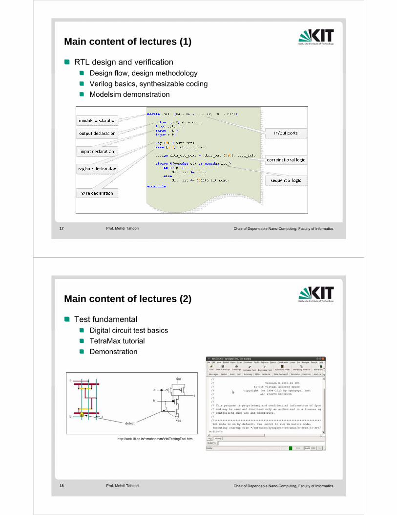
Main content of lectures (1)
RTL design and verificationDesign flow, design methodology
Verilog basics, synthesizable coding
Modelsim demonstration
Prof. Mehdi Tahoori
Chair of Dependable Nano-Computing, Faculty of Informatics18
Main content of lectures (2)
Test fundamentalDigital circuit test basics
TetraMax tutorial
Demonstration
Prof. Mehdi Tahoori
http://web.iiit.ac.in/~mohanbvm/VlsiTestingTool.htm

Chair of Dependable Nano-Computing, Faculty of Informatics19
Lab tasks and arrangements
Session 1 ~ 2Verilog design of a simple ALU
Session 3Logic synthesis of designed ALU
Session 4 ATPG and fault simulation about the synthesized ALU
Prof. Mehdi Tahoori
Chair of Dependable Nano-Computing, Faculty of Informatics20
Block3 : Circuit level design
We will focus on transistor level design
HSPICE simulations of CMOS gate
Motivation:Scaling the technology → everything becomes analogue
More accurate simulationsPower measurement of basic cells
Delay measurement of basic cells
Optimize basic cells for meet in the middle strategyFor area, delay and power
Physics based analysis is possibleProcess Variation analysis
Reliability analysis
Prof. Mehdi Tahoori

Chair of Dependable Nano-Computing, Faculty of Informatics21
Behavioral Domain
Prof. Mehdi Tahoori
Chair of Dependable Nano-Computing, Faculty of Informatics22
Introduction of CMOS technology
MOSFETMOS : Metal Oxide Semiconductor
FET: Field Effect transistor
CMOS: Complementary MOS:which means using both NMOS and PMOS transistors to form a circuit.
Transistors are not ideal switches.NMOS cannot transfer VDD ideally
And PMOS cannot transfer 0 ideally.
CMOS inverter:
Prof. Mehdi Tahoori

Chair of Dependable Nano-Computing, Faculty of Informatics23
Main tasks in Block3
Introducing the structure of basic CMOS cellsWhat are the challenges
How to overcome
Use Hspice as analogue simulator for basic cells:Design
Verify the functionalityDC analysis
Transient analysis
Delay measurement
Power measurement
Basic cells areSimple structures: NOT, NAND, NOR
More complex structures: Full Adder and Ripple Carry Adder
Main tools:Hspice
Prof. Mehdi Tahoori
Chair of Dependable Nano-Computing, Faculty of Informatics24
Dates ???
As a block Lab (recommended)At the end of the semester
5 full days from 16-20 July
Wednesdays 14:00 – 18:00 or
Thursdays 14:00 – 18:00
Prof. Mehdi Tahoori