digital current balancing for an interleaved boost pfc · 19 analog applications journal texas...
TRANSCRIPT
19
Analog Applications Journal
Texas Instruments Incorporated
2Q 2013 www.ti.com/aaj High-Performance Analog Products
Digital current balancing for an interleaved boost PFC
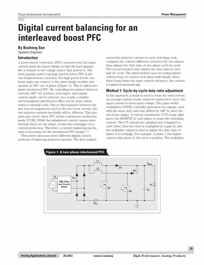
IntroductionA power-factor correction (PFC) converter lets the input current track the input voltage so that the load appears like a resistor to the voltage source that powers it. The most popular power topology used in active PFC is the non-isolated boost converter. For high power levels, two boost units can connect to the same bridge rectifier and operate at 180° out of phase (Figure 1). This is called two-phase interleaved PFC. By controlling two phases’ inductor currents 180° out of phase, both input- and output- current ripple can be reduced. As a result, a smaller electromagnetic-interference filter can be used, which reduces material costs. Due to discrepancies between the two sets of components used in the two boost circuits, the two inductor currents inevitably will be different. This situ-a tion gets worse when PFC enters continuous-conduction mode (CCM). While the unbalanced current causes more thermal stress on one phase, it may also mistrigger over-current protection. Therefore, a current-balancing mecha-nism is necessary for the interleaved PFC design.1–4
This article discusses three different digital-control methods of bal ancing inductor currents. The first method
senses the inductor current on each switching cycle, compares the current difference between the two phases, then adjusts the duty ratio of one phase cycle-by-cycle. The second method only adjusts the duty ratio in each half AC cycle. The third method uses two independent current loops to control each phase individually. Since these loops share the same current reference, the current is balanced automatically.
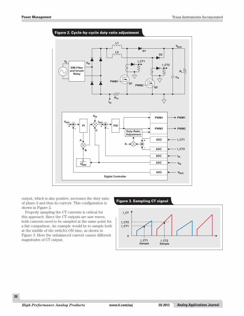
Method 1: Cycle-by-cycle duty-ratio adjustmentIn this approach, a shunt is used to sense the total current. An average-current mode control is employed to force the input current to track input voltage. The pulse-width- modulation (PWM) controller generates two signals, each with the same duty ratio but shifted by 180° to drive the two boost stages. A current transformer (CT) is put right above the MOSFET in each phase to sense the switching current. The CT outputs are sampled and compared to each other; then the error is multiplied by a gain K, and the multiplier output is used to adjust the duty ratio of phase 2 accordingly. For example, if phase 1 has higher current than phase 2, the error is positive. The multiplier
Power Management
By Bosheng SunSystems Engineer
VS
RS1
RL
Q1CB
VIN
D1
D2L2
L1
EMI Filterand Inrush
Relay
Q2
VBUS
Figure 1. A two-phase interleaved PFC
Texas Instruments Incorporated
20
Analog Applications JournalHigh-Performance Analog Products www.ti.com/aaj 2Q 2013
Power Management
output, which is also positive, increases the duty ratio of phase 2 and thus its current. This configuration is shown in Figure 2.
Properly sampling the CT currents is critical for this approach. Since the CT outputs are saw waves, both currents need to be sampled at the same point for a fair comparison. An example would be to sample both at the middle of the switch’s ON time, as shown in Figure 3. Here the unbalanced current causes different magnitudes of CT output.
IIN
PWM2
VBUS
Q1
PWM1
D1
D2L2
L1
PI PID+ +– –
VREF IREF
A
B
C
+ +
KM
PWM1
PWM1
PWM2
VBUS
VIN
IIN
ADC I_CT1
I_CT2
Digital Controller
Duty-RatioAdjustment
K
I_CT1
I_CT2EMI Filter
and InrushRelay
Q2PWM2
+
–+
1
VRMS2
ADC
ADC
ADC
ADC
VS VIN
RL
CB
RS1
Figure 2. Cycle-by-cycle duty-ratio adjustment
I_CT1Sample
I_CT2Sample
I_CT
I_CT2
I_CT1
0
Figure 3. Sampling CT signal
Texas Instruments Incorporated
21
Analog Applications Journal 2Q 2013 www.ti.com/aaj High-Performance Analog Products
Power Management
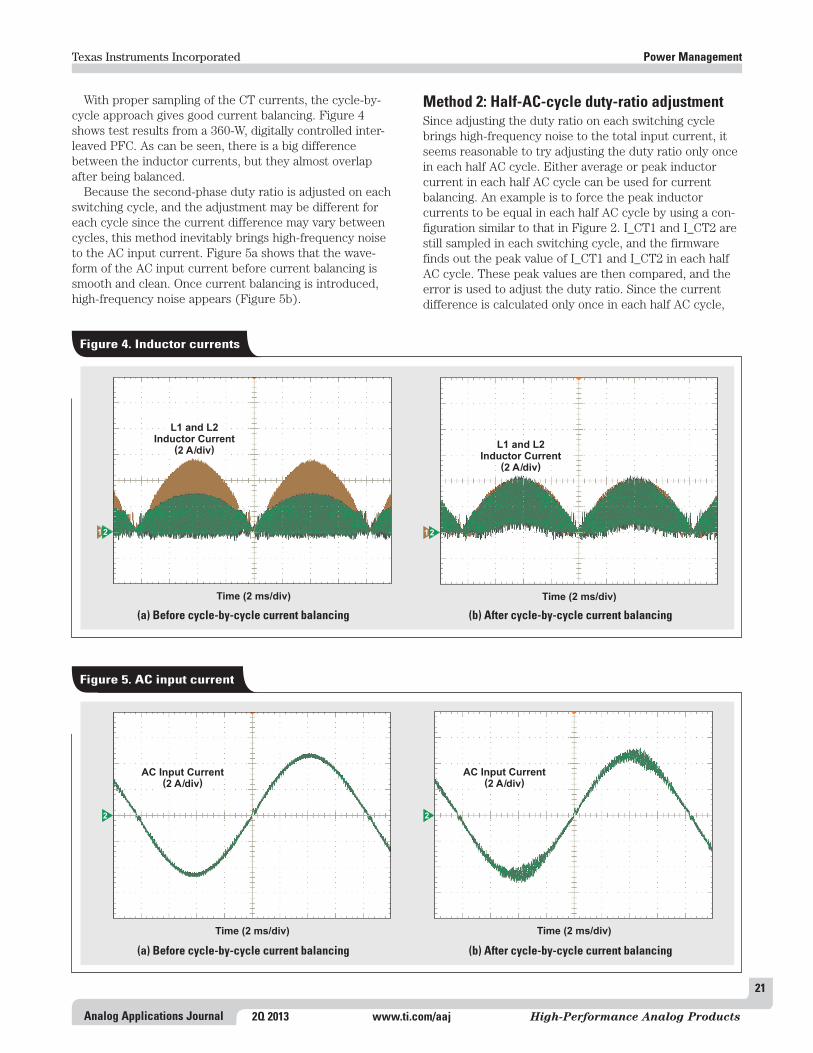
With proper sampling of the CT currents, the cycle-by-cycle approach gives good current balancing. Figure 4 shows test results from a 360-W, digitally controlled inter-leaved PFC. As can be seen, there is a big difference between the inductor currents, but they almost overlap after being balanced.
Because the second-phase duty ratio is adjusted on each switching cycle, and the adjustment may be different for each cycle since the current difference may vary between cycles, this method inevitably brings high-frequency noise to the AC input current. Figure 5a shows that the wave-form of the AC input current before current balancing is smooth and clean. Once current balancing is introduced, high-frequency noise appears (Figure 5b).
Method 2: Half-AC-cycle duty-ratio adjustmentSince adjusting the duty ratio on each switching cycle brings high-frequency noise to the total input current, it seems reasonable to try adjusting the duty ratio only once in each half AC cycle. Either average or peak inductor current in each half AC cycle can be used for current balancing. An example is to force the peak inductor currents to be equal in each half AC cycle by using a con-figuration similar to that in Figure 2. I_CT1 and I_CT2 are still sampled in each switching cycle, and the firmware finds out the peak value of I_CT1 and I_CT2 in each half AC cycle. These peak values are then compared, and the error is used to adjust the duty ratio. Since the current difference is calculated only once in each half AC cycle,
1
Time (2 ms/div)
2
L1 and L2Inductor Current
(2 A/div)
Figure 4. Inductor currents
1
Time (2 ms/div)
2
L1 and L2Inductor Current
(2 A/div)
(a) Before cycle-by-cycle current balancing (b) After cycle-by-cycle current balancing
Time (2 ms/div)
2
AC Input Current(2 A/div)
Figure 5. AC input current
Time (2 ms/div)
2
AC Input Current(2 A/div)
(a) Before cycle-by-cycle current balancing (b) After cycle-by-cycle current balancing
Texas Instruments Incorporated
22
Analog Applications JournalHigh-Performance Analog Products www.ti.com/aaj 2Q 2013
Power Management
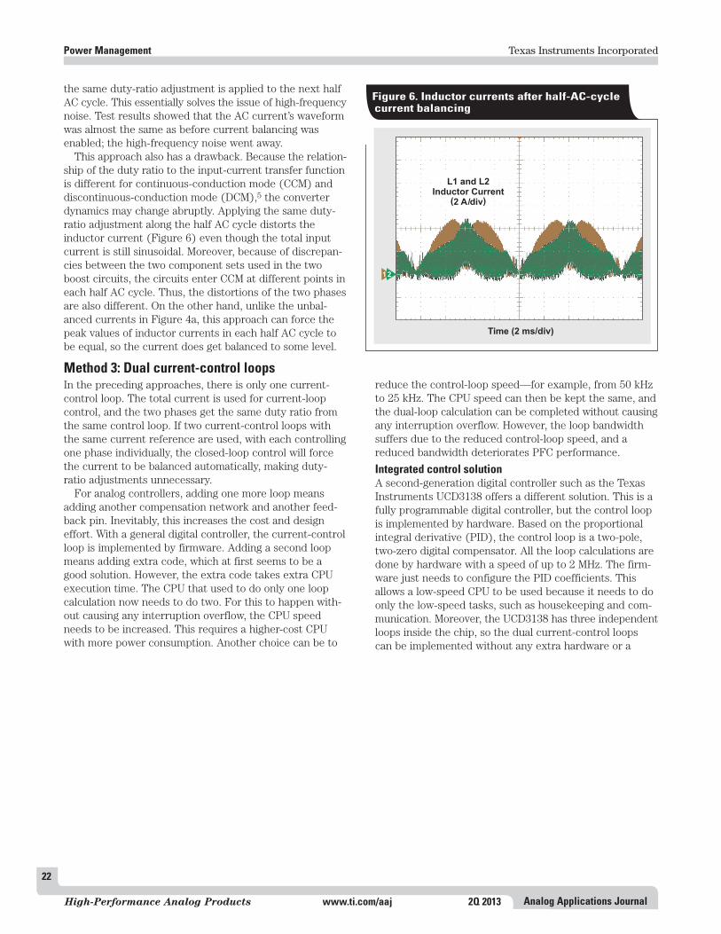
the same duty-ratio adjustment is applied to the next half AC cycle. This essentially solves the issue of high-frequency noise. Test results showed that the AC current’s waveform was almost the same as before current balancing was enabled; the high-frequency noise went away.
This approach also has a drawback. Because the rela tion-ship of the duty ratio to the input-current transfer function is different for continuous-conduction mode (CCM) and discontinuous-conduction mode (DCM),5 the converter dynamics may change abruptly. Applying the same duty-ratio adjustment along the half AC cycle distorts the inductor current (Figure 6) even though the total input current is still sinusoidal. Moreover, because of discrepan-cies between the two component sets used in the two boost circuits, the circuits enter CCM at different points in each half AC cycle. Thus, the distortions of the two phases are also different. On the other hand, unlike the unbal-anced currents in Figure 4a, this approach can force the peak values of inductor currents in each half AC cycle to be equal, so the current does get balanced to some level.
Method 3: Dual current-control loopsIn the preceding approaches, there is only one current-control loop. The total current is used for current-loop control, and the two phases get the same duty ratio from the same control loop. If two current-control loops with the same current reference are used, with each controlling one phase individually, the closed-loop control will force the current to be balanced automatically, making duty-ratio adjustments unnecessary.
For analog controllers, adding one more loop means adding another compensation network and another feed-back pin. Inevitably, this increases the cost and design effort. With a general digital controller, the current-control loop is implemented by firmware. Adding a second loop means adding extra code, which at first seems to be a good solution. However, the extra code takes extra CPU execution time. The CPU that used to do only one loop calculation now needs to do two. For this to happen with-out causing any interruption overflow, the CPU speed needs to be increased. This requires a higher-cost CPU with more power consumption. Another choice can be to
reduce the control-loop speed—for example, from 50 kHz to 25 kHz. The CPU speed can then be kept the same, and the dual-loop calculation can be completed without causing any interruption overflow. However, the loop bandwidth suffers due to the reduced control-loop speed, and a reduced bandwidth deteriorates PFC performance.
Integrated control solutionA second-generation digital controller such as the Texas Instruments UCD3138 offers a different solution. This is a fully programmable digital controller, but the control loop is implemented by hardware. Based on the proportional integral derivative (PID), the control loop is a two-pole, two-zero digital compensator. All the loop calculations are done by hardware with a speed of up to 2 MHz. The firm-ware just needs to configure the PID coefficients. This allows a low-speed CPU to be used because it needs to do only the low-speed tasks, such as housekeeping and com-munication. Moreover, the UCD3138 has three independent loops inside the chip, so the dual current-control loops can be implemented without any extra hardware or a
1
Time (2 ms/div)
2
L1 and L2Inductor Current
(2 A/div)
Figure 6. Inductor currents after half-AC-cycle current balancing
Texas Instruments Incorporated
23
Analog Applications Journal 2Q 2013 www.ti.com/aaj High-Performance Analog Products
Power Management
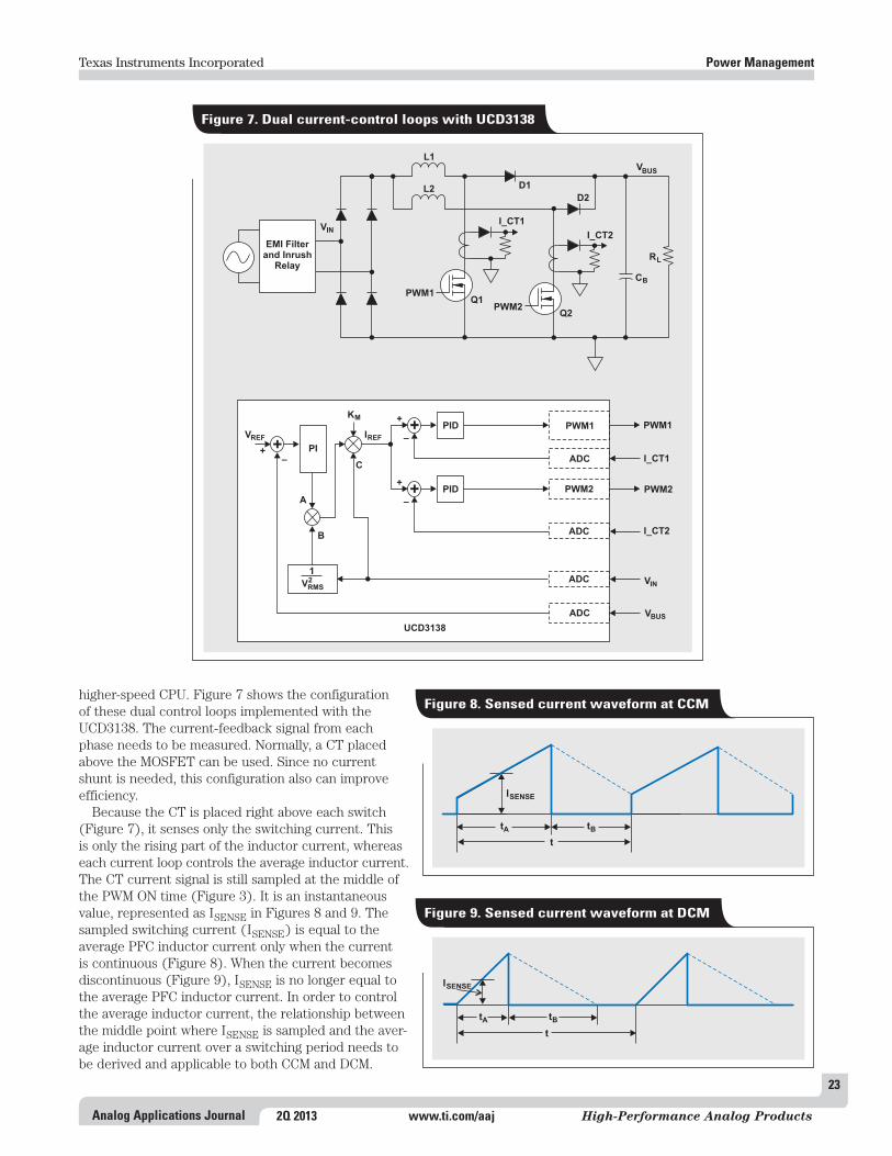
higher-speed CPU. Figure 7 shows the configuration of these dual control loops implemented with the UCD3138. The current-feedback signal from each phase needs to be measured. Normally, a CT placed above the MOSFET can be used. Since no current shunt is needed, this configuration also can improve efficiency.
Because the CT is placed right above each switch (Figure 7), it senses only the switching current. This is only the rising part of the inductor current, whereas each current loop controls the average inductor current. The CT current signal is still sampled at the middle of the PWM ON time (Figure 3). It is an instantaneous value, represented as ISENSE in Figures 8 and 9. The sampled switching current (ISENSE) is equal to the average PFC inductor current only when the current is continuous (Figure 8). When the current becomes discontinuous (Figure 9), ISENSE is no longer equal to the average PFC inductor current. In order to control the average inductor current, the relationship between the middle point where ISENSE is sampled and the aver-age inductor current over a switching period needs to be derived and applicable to both CCM and DCM.
VBUS
Q1
PWM1
D1
D2L2
L1
PI+–
VREF IREF
A
B
C
+
KM
PWM1
PWM1
PWM2PWM2
VBUS
VIN
ADC I_CT1
I_CT2
UCD3138
I_CT1
I_CT2EMI Filter
and InrushRelay
Q2PWM2
1
VRMS2
ADC
ADC
ADC
VIN
RL
CB
PID+
–+
PID+
–+
Figure 7. Dual current-control loops with UCD3138
ISENSE
tA
t
tB
Figure 8. Sensed current waveform at CCM
t
ISENSE
tA tB
Figure 9. Sensed current waveform at DCM
Texas Instruments Incorporated
24
Analog Applications JournalHigh-Performance Analog Products www.ti.com/aaj 2Q 2013
Power Management
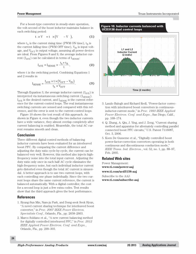
For a boost-type converter in steady-state operation, the volt-second of the boost inductor maintains balance in each switching period:
( )˙˙˙˙t V t V V ,× = × − (1)
where tA is the current rising time (PWM ON time), tB is the current falling time (PWM OFF time), VIN is input volt-age, and VOUT is output voltage, assuming all power devices are ideal. From Figures 8 and 9, the average inductor cur-rent (IAVE) can be calculated in terms of ISENSE:
A BAVE SENSE
t tI I ,
t
+= × (2)
where t is the switching period. Combining Equations 1 and 2 results in
( )AVE OUT INSENSE
A OUT
I t V VI .
t V
× × −=
× (3)
Through Equation 3, the average inductor current (IAVE) is interpreted via instantaneous switching current (ISENSE). IAVE is the desired current, and ISENSE is the current refer-ence for the current-control loops. The real instantaneous switching currents are sensed and compared with this ref-erence, and the error is sent to the current-control loops.
Figure 10 shows the test result of this approach. As shown in Figure 4, even though the two inductor currents have a wide variance, they almost overlap completely after current balancing is enabled. Meanwhile, the total AC cur-rent remains smooth and clean.
ConclusionThree different digital-control methods of balancing inductor currents have been evaluated for an interleaved boost PFC. By comparing the current difference and adjusting the duty ratio cycle-by-cycle, the current can be balanced very well. However, this method also injects high- frequency noise into the total input current. Adjusting the duty ratio only once in each half AC cycle eliminates the high-frequency noise, but each individual inductor current gets distorted even though the total AC current is sinusoi-dal. A better approach is to use two current loops, with each controlling one phase individually. Since the two cur-rent loops share the same current reference, the current is balanced automatically. With a digital controller, the cost for a second loop is just a few extra codes. Test results show that the third approach gives the best performance.
References1. Byung-Sun Min, Nam-ju Park, and Dong-seok Seok Hyun,
“A novel current sharing technique for interleaved boost converter,” in Proc. 2007 IEEE Power Electron. Specialists Conf., Orlando, Fla., pp. 2658–2663.
2. Marco Soldano et al., “A new current balancing method for digitally controlled interleaved PFC,” in Proc. 2012 IEEE Applied Power Electron. Conf. and Expo., Orlando, Fla., pp. 299–303.
3. Laszlo Balogh and Richard Redl, “Power-factor correc-tion with interleaved boost converters in continuous-inductor-current mode,” in Proc. 1993 IEEE Applied Power Electron. Conf. and Expo., San Diego, Calif., pp. 168–174.
4. Q. Zhang, A. Qiu, J. Ying, and J. Zeng, “Current sharing method and apparatus for alternately controlling parallel connected boost PFC circuits,” U.S. Patent 7116087, Oct. 3, 2006.
5. Koen De Gusseme et al., “Digitally controlled boost power-factor-correction converters operating in both continuous and discontinuous conduction mode,” IEEE Trans. Ind. Electron., vol. 52, no. 1, pp. 88–97, Feb. 2005.
Related Web sitesPower Management:www.ti.com/power-aaj
www.ti.com/ucd3138-aaj
Subscribe to the AAJ:www.ti.com/subscribe-aaj
1
Time (2 ms/div)
2
L1 and L2Inductor Current
(2 A/div)
Figure 10. Inductor currents balanced with UCD3138 dual control loops
© 2013 Texas Instruments Incorporated
E2E is a trademark of Texas Instruments. All other trademarks are the property of their respective owners.
SLYT517
TI Worldwide Technical Support
InternetTI Semiconductor Product Information Center Home Pagesupport.ti.com
TI E2E™ Community Home Pagee2e.ti.com
Product Information CentersAmericas Phone +1(512) 434-1560
Brazil Phone 0800-891-2616
Mexico Phone 0800-670-7544
Fax +1(972) 927-6377 Internet/Email support.ti.com/sc/pic/americas.htm
Europe, Middle East, and AfricaPhone European Free Call 00800-ASK-TEXAS (00800 275 83927) International +49 (0) 8161 80 2121 Russian Support +7 (4) 95 98 10 701
Note: The European Free Call (Toll Free) number is not active in all countries. If you have technical difficulty calling the free call number, please use the international number above.
Fax +(49) (0) 8161 80 2045Internet www.ti.com/asktexasDirect Email [email protected]
JapanPhone Domestic 0120-92-3326
Fax International +81-3-3344-5317 Domestic 0120-81-0036
Internet/Email International support.ti.com/sc/pic/japan.htm Domestic www.tij.co.jp/pic
AsiaPhone International +91-80-41381665 Domestic Toll-Free Number Note: Toll-free numbers do not support
mobile and IP phones. Australia 1-800-999-084 China 800-820-8682 Hong Kong 800-96-5941 India 1-800-425-7888 Indonesia 001-803-8861-1006 Korea 080-551-2804 Malaysia 1-800-80-3973 New Zealand 0800-446-934 Philippines 1-800-765-7404 Singapore 800-886-1028 Taiwan 0800-006800 Thailand 001-800-886-0010Fax +8621-23073686Email [email protected] or [email protected] support.ti.com/sc/pic/asia.htm
A090712
Important Notice: The products and services of Texas Instruments Incorporated and its subsidiaries described herein are sold subject to TI’s standard terms and conditions of sale. Customers are advised to obtain the most current and complete information about TI products and services before placing orders. TI assumes no liability for applications assistance, customer’s applications or product designs, software performance, or infringement of patents. The publication of information regarding any other company’s products or services does not constitute TI’s approval, warranty or endorsement thereof.
IMPORTANT NOTICE
Texas Instruments Incorporated and its subsidiaries (TI) reserve the right to make corrections, enhancements, improvements and otherchanges to its semiconductor products and services per JESD46, latest issue, and to discontinue any product or service per JESD48, latestissue. Buyers should obtain the latest relevant information before placing orders and should verify that such information is current andcomplete. All semiconductor products (also referred to herein as “components”) are sold subject to TI’s terms and conditions of salesupplied at the time of order acknowledgment.
TI warrants performance of its components to the specifications applicable at the time of sale, in accordance with the warranty in TI’s termsand conditions of sale of semiconductor products. Testing and other quality control techniques are used to the extent TI deems necessaryto support this warranty. Except where mandated by applicable law, testing of all parameters of each component is not necessarilyperformed.
TI assumes no liability for applications assistance or the design of Buyers’ products. Buyers are responsible for their products andapplications using TI components. To minimize the risks associated with Buyers’ products and applications, Buyers should provideadequate design and operating safeguards.
TI does not warrant or represent that any license, either express or implied, is granted under any patent right, copyright, mask work right, orother intellectual property right relating to any combination, machine, or process in which TI components or services are used. Informationpublished by TI regarding third-party products or services does not constitute a license to use such products or services or a warranty orendorsement thereof. Use of such information may require a license from a third party under the patents or other intellectual property of thethird party, or a license from TI under the patents or other intellectual property of TI.
Reproduction of significant portions of TI information in TI data books or data sheets is permissible only if reproduction is without alterationand is accompanied by all associated warranties, conditions, limitations, and notices. TI is not responsible or liable for such altereddocumentation. Information of third parties may be subject to additional restrictions.
Resale of TI components or services with statements different from or beyond the parameters stated by TI for that component or servicevoids all express and any implied warranties for the associated TI component or service and is an unfair and deceptive business practice.TI is not responsible or liable for any such statements.
Buyer acknowledges and agrees that it is solely responsible for compliance with all legal, regulatory and safety-related requirementsconcerning its products, and any use of TI components in its applications, notwithstanding any applications-related information or supportthat may be provided by TI. Buyer represents and agrees that it has all the necessary expertise to create and implement safeguards whichanticipate dangerous consequences of failures, monitor failures and their consequences, lessen the likelihood of failures that might causeharm and take appropriate remedial actions. Buyer will fully indemnify TI and its representatives against any damages arising out of the useof any TI components in safety-critical applications.
In some cases, TI components may be promoted specifically to facilitate safety-related applications. With such components, TI’s goal is tohelp enable customers to design and create their own end-product solutions that meet applicable functional safety standards andrequirements. Nonetheless, such components are subject to these terms.
No TI components are authorized for use in FDA Class III (or similar life-critical medical equipment) unless authorized officers of the partieshave executed a special agreement specifically governing such use.
Only those TI components which TI has specifically designated as military grade or “enhanced plastic” are designed and intended for use inmilitary/aerospace applications or environments. Buyer acknowledges and agrees that any military or aerospace use of TI componentswhich have not been so designated is solely at the Buyer's risk, and that Buyer is solely responsible for compliance with all legal andregulatory requirements in connection with such use.
TI has specifically designated certain components as meeting ISO/TS16949 requirements, mainly for automotive use. In any case of use ofnon-designated products, TI will not be responsible for any failure to meet ISO/TS16949.
Products Applications
Audio www.ti.com/audio Automotive and Transportation www.ti.com/automotive
Amplifiers amplifier.ti.com Communications and Telecom www.ti.com/communications
Data Converters dataconverter.ti.com Computers and Peripherals www.ti.com/computers
DLP® Products www.dlp.com Consumer Electronics www.ti.com/consumer-apps
DSP dsp.ti.com Energy and Lighting www.ti.com/energy
Clocks and Timers www.ti.com/clocks Industrial www.ti.com/industrial
Interface interface.ti.com Medical www.ti.com/medical
Logic logic.ti.com Security www.ti.com/security
Power Mgmt power.ti.com Space, Avionics and Defense www.ti.com/space-avionics-defense
Microcontrollers microcontroller.ti.com Video and Imaging www.ti.com/video
RFID www.ti-rfid.com
OMAP Applications Processors www.ti.com/omap TI E2E Community e2e.ti.com
Wireless Connectivity www.ti.com/wirelessconnectivity
Mailing Address: Texas Instruments, Post Office Box 655303, Dallas, Texas 75265Copyright © 2013, Texas Instruments Incorporated