digital communications lab -...
TRANSCRIPT

Microwave and Digital communication Lab
1
DIGITAL COMMUNICATIONS LAB
List of Experiments:
1. PCM Generation and Detection.
2. Differential Pulse Code modulation.
3. Delta modulation.
4. Time Division Multiplexing of 2band Limited Signals.
5. Frequency Shift Keying: Generation and Detection.
6. Phase Shift Keying: Generation and Detection.
7. Amplitude shift Keying: Generation and Detection.
8. Study of the spectral characteristics of PAM, QAM.
9. DPSK: Generation and Detection.
10. QPSK: Generation and Detection.
Note: (Any 6 Experiments)

Microwave and Digital communication Lab
2
Expt No: 1
PULSE CODE MODULATION AND DEMODULATION
AIM: To Study & understand the operation of the Pulse code modulation &
Demodulation.
APPARATUS:
1. PCM Modulator trainer
2. PCM Demodulator trainer
3. Storage Oscilloscope/ Dual Trace Oscilloscope
(Note: Storage oscilloscope is desired for satisfactory observation of PCM
wave forms)
4. Digital multimeter.
5. 2 No.’s of co-axial cables (standard accessories with trainer)
6. patch chords
7.
CIRCUIT DIAGRAM:

Microwave and Digital communication Lab
3
THEORY:
Pulse modulation: A form of modulation in which a pulse train is used as the carrier.
Information is conveyed by modulating some parameter of the pulses with a set of
discrete instantaneous samples of the messages signal. The minimum sampling
frequency is the minimum frequency at which the modulating waveform can be
sampled to provide the set of discrete values without a significant loss of information.
PCM: In pulse code modulation (PCM) only certain discrete values are allowed for
the modulating signals. The modulating signal sampled, as in other forms of pulse
modulation. But any sample falling within a specified range of values is assigned a
discrete value. Each value is assigned a pattern of pulses and the signal transmitted by
means of this code. The electronic circuit that produces the coded pulse train from the
modulating waveform is termed a coder or encoder. A suitable decoder must be used
at the receiver in order to extract the original information from the transmitted pulse
train.
PROCEDURE:
1. Study the theory of operation thoroughly.
2. Connect the trainer (Modulator) to the mains and switch on the power supply.
3. Observe the output of the AF generator using CRO, it should be a Sine wave
of 200Hz frequency with 3Vpp amplitude.
4. Verify the output of the DC source with multimeter / scope, output should
vary 0 to +5v.
5. Observe the output of the Clock generator using CRO, they should be 64KHz
and 4KHz frequency of square wave with 5 Vp amplitude.
Note: These clock signals are internally connected the circuit so no external
connections are required.
6. Connect the trainer (De Modulator) to the mains and switch on the power
supply.
7. Observe the output of the clock generator using CRO, it should be 64 KHz
square wave with 5 Vp-p amplitude.

Microwave and Digital communication Lab
4
PCM Operation (with DC input)
Modulation:
8. Set DC source to some value say 1 V with the help of multimeter and connect
it to the A/D converter input and observe the output LED’s.
9. Note down the digital code i.e output of the A/D converter and compare with
the theoretical value
Theoretical value can be obtained by:
A/D input voltage
________________ = X(10) = Y(2)
1 LSB value
Where
1 LSB value = Vref / 2n
Since Vref = 5V and n= 8
1 LSB Value = 0.01953
Example:
A/D input voltage = 1 V
= 51.2(10)
= 00110011(2)
So digital output is 00110011
10. Keep CRO in dual mode. Connect one channel to 4KHz signal ( which is
connected to the shift register) and another channel to the PCM out put
11. Observe the PCM output with respect to the 4KHz signal and sketch the
waveforms. Compare them with the given waveforms
Note: From this wave form you can observe that the LSB bit enters the output
first.
Demodulation:
12. Connect PCM signal to the demodulators (S-P Shift register) from the PCM
modulator (AET-68M) with help of coaxial cable (supplied with the trainer)
13. Connect clock signal (64 KHz) from the transmitter to the receiver using
coaxial cable.
14. Connect transmitter clock to the timing circuit
15. Observe and note down the S-P shift register output data and compare it with
the transmitted data (i.e output A/D converter at transmitter). You will notice
that the output of the S-P shift register is following the A/D converter output

Microwave and Digital communication Lab
5
in the modulator. Observe D/A converter output (demodulated output) using
multimeter /scope and compare it with the original signal and you can observe
that there is no loss in information in process of conversion and transmission.
16. Similarly you can try for different values of modulating signal voltage.
Sample work sheet:
1. Modulating signal : 1V
2. A/D output (theoretical) : 00 11 00 11(2)
3. A/D output (practical) : 00 11 00 11(2)
4. S-P output : 00 11 00 11(2)
5. D/A Converter output : 1V
(Demodulation output)
PCM Operation (with AC input)
Modulation:
17. Connect AC signal of 2VPP amplitude to Sample & Hold circuit.
18. Keep the CRO in dual mode. Connect one channel to the AF signal and
another channel to the sample & hold output. Observe and sketch the sample
& hold output.
19. Connect the sample and hold output to the A/D converter and observe the
PCM output using storage oscilloscope/ DTO
20. Observe PCM output by varying AF signal voltage.
Demodulation
21. Connect PCM signal to the demodulator input (S-P shift register) from the
PCM modulator with the help of coaxial cable (supplied with the trainer)
22. Connect clock signal (64KHz) from the transmitter to the receiver using
coaxial cable
23. Connect transmitter clock to the timing circuit.
24. Keep CRO in dual mode. Connect CH 1 input to the sample and hold output
and CH 2 input ot the D/A converter output .
25. Observe and sketch the D/A output.
26. Connect D/A output to the LPF input.
27. Observe output of the LPF/Amplifier and compare it with the original
modulating signal .
28. From above observation you can verify that there is no loss in information
(modulating signal) in conversion and transmission process.

Microwave and Digital communication Lab
6
29. Disconnect clock from transmitter and connect to local oscillator (i.e. clock
generator output from Demodulator) with remaining setup as it is. Observe
D/A output and compare it with the previous result. This signal is little bit
distorted in shape. This is because lack of synchronization between clock at
transmitter and clock at receiver.
Note: You can take modulating signals from external sources. Maximum
amplitude should not exceed 4V incase of DC and 3VPP in case of AC (AF)
signals.
EXPECTED WAVEFORMS:

Microwave and Digital communication Lab
7
PCM wave forms / timing diagram of DC input
Input signal +1 v
Gnd. _______________________________________________________________
Clock 1 (64 KHz)
Clock 2 (4 KHz)
+ 5v
Gnd
11 11 11 11
00 00 0 0
0 0
A/D Output 0101 (Led Indication MSB to LSB)
DPCM signal
S – P : Register output 0101 (Led Indication MSB to LSB)
D/A output (demodulated signal)
+1 v
Gnd
______________________________________________________________
_

Microwave and Digital communication Lab
8
RESULT:
QUESTIONS:
1. Differentiate PCM over Analog modulation?
2. What is bit synchronization & frame synchronization?
3. Explain block diagram of PCM?
4. What is the different error control coding technique?
5. What is resolution in ADC?
6. For arbitrary fixed reference voltage write the table of 4-bit ADC?
7. The accuracy of any digital reproduction of an analog signal depends on what?
8. If sample requires at least 12 levels of precision (+0 to +5 and –0 to –5). How many
bits should be sent for each sample? use one bit form sign.
9. What is the formula for bit rate in PCM?
10. If we want to digitize human voice (4 KHz B.W), what is the bit rate assuming 8
Bits/sample?
11. What is the sampling rate for PCM if the frequency ranges from 1000Hz to
4000Hz?
12. If the interval between two samples in a digital signal is 125 micro seconds. What
is the sampling rate?

Microwave and Digital communication Lab
9
Expt No: 2
DIFFERENTIAL PULSE CODE MODULATION AND DEMODULATION
AIM: To Study & understand the operation of the DPCM
APPARATUS:
1. DPCM Modulator trainer
2. DPCM Demodulator trainer
3. Storage Oscilloscope
4. Digital Multimeter.
5.2 No’s of co- axial cables (standard accessories with trainer)
6. Patch chords
THEORY:
Differential PCM is quite similar to ordinary PCM. However, each word in
this system indicates the difference in amplitude, positive or negative, between this
sample and the previous sample. Thus the relative value of each sample is indicated
rather than, the absolute value as in normal PCM.
This unique system consists of
BLOCK DIAGRAM:

Microwave and Digital communication Lab
10
I. DPCM Modulator
1. Regulated power supply
2. Audio Frequency signal generator
3. Prediction Filter
4. Sample & Hold circuit
5. A/D Converter
6. Parallel –Serial Shift register
7. Clock generator / Timing circuit
8. DC source
II. DPCM Demodulator
1. Regulated Power Supply
2. Serial-Parallel Shift registers.
3. D/A converter.
4. Clock generator
5. Timing circuit
6. Prediction filter
7. Passive low pass filter
PROCEDURE:
1. Study the theory of operation thoroughly.
2. Connect the trainer (Modulator) to the mains and switch on the power supply.
3. Observe the output of the AF generator using CRO, it should be Sine wave of
400 Hz frequency with 3V pp amplitude.
4. Verify the output of the DC source with multimeter/scope; output should vary
0 to +290mV.
5. Observe the output of the Clock generator using CRO, they should be 64 KHz
and 8 KHz frequency of square with 5 Vp-p amplitude.
6. Connect the trainer (De Modulator) to the mains and switch on the power
supply.
7. Observe the output of the Clock generator using CRO; it should be 64 KHz
square wave with amplitude of 5 pp.

Microwave and Digital communication Lab
11
DPCM Operation (with DC input):
Modulation:
1. Keep CRO in dual mode. Connect one channel to 8 KHz signal (one which is
connected to the Shift register) and another channel to the DPCM output.
2. Observe the DPCM output with respect to the 8 KHz signal and sketch the
Waveforms.
Note: Form this waveform you can observe that the LSB bit enters the output
First.
Demodulation
3. Connect DPCM signal to the demodulator (S-P register) from the DPCM
modulator with the help of coaxial cable (supplied with the trainer).
4. Connect clock signal (64 KHz) from the transmitter to the receiver using
coaxial cable.
5. Connect transmitter clock to the timing circuit.
6. Observe and note down the S-P shift register output data and compare it with
the transmitted data (i.e. output A/D converter at transmitter) notice that the
output of the S-P shift register is following the A/D converter output in the
modulator.
7. Observe D/A converter output (demodulated output) using multimeter/scope
and compare it with the original signal and can observe that there is no loss in
information in process of conversion and transmission.
DPCM Operation (with AC input):
Modulation:
8. Connect AC signal of 3VPP amplitude to positive terminal of the summer
circuit.
Note: The output of the prediction filter is connected to the negative terminal of
the summer circuit and can observe the waveforms at the test points provided on
the board.
9. The output of the summer is internally connected to the sample and hold circuit
10. Keep CRO in dual mode. Connect one channel to the AF signal and another
channel to the Sample and Hold output. Observe and sketch the sample &
hold output

Microwave and Digital communication Lab
12
11. Connect the Sample and Hold output to the A/D converter and observe the
DPCM output using oscilloscope.
12. Observe DPCM output by varying AF signal voltage.
Demodulation:
13. Connect DPCM signal to the demodulator input (S-P shift register) from the
DPCM modulator with the help of coaxial cable (supplied with trainer).
14. Connect clock signal (64 KHz) from the transmitter to the receiver using
coaxial cable.
15. Connect transmitter clock to the timing circuit.
16. Keep CRO in dual mode. Connect one channel to the sample & hold output
and another channel to the D/A converter output.
17. Observe and sketch the D/A output
18. Connect D/A output to the LPF input and observe the output of the LPF.
19. Observe the wave form at the output of the summer circuit.
20. Disconnect clock from transmitter and connect to the local oscillator (i.e.,
clock generator output from Demodulator) with remaining setup as it is.
Observe D/A output and compare it with the previous result. This signal is
little bit distorted in shape. This is because lack of synchronization between
clock at transmitter and clock at receiver.

Microwave and Digital communication Lab
13
EXPECTED WAVEFORMS:
Draw the wave forms for the given DC input (190mV)corresponding binary
data wave form, and for AC input draw sample and hold waveform then D/A
converter o/p and then reconstructed AC signal
DPCM way form / timing diagram DC input
190mV
Input signal
Gnd. ______________________________________________________________ _
Clock 1 (64 KHz)
Clock 2 (8 KHz)
+ 5v
Gnd
1 1 1 1
0 0 0
0
A/D Output 0101 (Led Indication MSB to LSB)
DPCM signal
S – P : Register output 0101 (Led Indication MSB to LSB)
D/A output (demodulated signal)
190mV
Gnd
_____________________________________________________________
RESULT:

Microwave and Digital communication Lab
14
Expt No: 3
DELTA MODULATION AND DEMODULATION
AIM: To transmit an analog message signal in its digital form and again reconstruct
back the original analog message signal at receiver by using Delta modulator. APPARATUS:
Equipment required:
1. DM Modulator trainer
2. DM Demodulator trainer
3. Storage Oscilloscope
(Note: Storage oscilloscope is desired for satisfactory observation of DM wave
forms)
4. Digital multimeter.
5. 2 No’s co-axial cables (standard accessories with trainer)
THEORY: Introduction:
Pulse modulation: A form modulation in which a pulse train is used as the
carrier. Information is conveyed by modulating some parameter of the pulses with a
set of discrete instantaneous samples of the message signal. The minimum sampling
frequency is the minimum frequency at which the modulating waveform can be
sampled to provide the set of discrete values without a significant loss of information.
There are different forms of pulse modulations like pulse amplitude modulation
(PAM), pulse width modulation (PWM), pulse position modulation (PPM). In PAM
the amplitude of the pulses is modulated by the corresponding samples of the
modulating wave. In PPM the samples are used to vary the time of occurrence of
some parameter of the pulses. In PWM the time of occurrence of the leading edge or
trailing edge is varied from its un-modulated position. All these types are un-coded
modulation.
PCM: in pulse code modulation (PCM) only certain discrete values are allowed for
the modulating signals. The modulating signal is sampled, as in other forms of pulse
modulation. But any sample falling within a specified range of values is assigned a
discrete value. Each value is assigned a pattern of pulses and the signal transmitted by
means of this code. The electronic circuit that produces the coded pulse train from the
modulating waveform is termed a coder or encoder. A suitable decoder must be used

Microwave and Digital communication Lab
15
at the receiver in order to extract the original information from the transmitted pulse
train.
DPCM: Differential PCM differs from the conventional PCM in the respect that here
only the relative amplitude of various samples ant not the absolute magnitude is
indicated. That is each word in this system indicates difference in amplitude between
this sample and the previous sample. The logic behind this approach is that there are
very little variations from sample to sample and the transmission of difference would
require only a fewer bits and hence a smaller bandwidth.
Encoding and decoding process in differential PCM tend to become very complicated
and it is because of these reasons that this system has not found wide acceptance.
DM: Delta modulation is almost similar to differential PCM. In this, only one bit is
transmitted per sample just to indicate whether the present sample is larger or smaller
than the previous one. The encoding, decoding and quantizing process become
extremely simple but this system cannot handle rapidly varying samples. This
increases quantizing noise. It has also not found wide acceptance.
Delta Modulation & Demodulation is a self sustained and well organized kit for the
demonstration of delta modulation & demodulation. Basic circuits those are well
known to every electronic student have been used in this trainer system. And this is
absolute practical implementation of delta modulation theory which we come across
in class room. This unique system consists of:
DM Modulator:
Regulated power supply.
Audio Frequency signal generator.
Buffer/Signal shaping network.
Voltage comparator.
4 Bit UP/DOWN Counter.
Clock generator/ Timing circuit.
4 Bit D/A converter.
DC source.
DM Demodulator:
Regulated power supply.
4 Bit UP/DOWN Counter.
4 Bit D/A converter.
Clock generator.
Passive low pass filter.
Audio amplifier.

Microwave and Digital communication Lab
16
EXPERIMENTAL PROCEDURE:
DM Modulator:
1. Study the theory of operation.
2. Connect the trainer (DM Modulator) to the mains and switch on the power
supply.
3. Observe the output of the AF generator using CRO, it should be a Sine wave
of 100 Hz frequency with 3Vpp amplitude.
4. Verify the output of the DC source with multimeter/scope; output should vary
0 to +4v.
5. Observe the output of the Clock generator using CRO, they should be 4 KHz
frequency of square wave with 5 Vpp amplitude.
Note: This clock signal is internally connected to the up/down counter so no
external connection is required
DM With DC Voltage as modulating signal:
1. Connect dc signal from the DC source to the inverting input of the
comparator and set some voltage say 3V.
2. Observe and plot the signals at D/A converter output (i.e., non-inverting
input of the comparator), DM signal using CRO and compare them with
the wave forms given in figure1:2.
Connect DM signal (from Modulator) to the DM input of the demodulator
1. Connect clock (4 KHz) from modulator to the clock input of the
demodulator. Connect clock input of the UP/DOWN counter to the clock
from transmitter with the help of springs provided.
2. Observe digital output (LED Indication) of the UP/DOWN counter and
compare it with the output of the UP/DOWN. By this you can notice that
the both the outputs are same.
3. Observe and plot the output of the D/A converter and compare it with the
wave forms given in Figure 1:2.
4. Measure the demodulated signal (i.e. output of the D/A converter with the
help of multimeter and compare it with the original signal.
5. From above observation you can notice that the both the voltages are equal
and there is no loss in process of modulation, transmission and
demodulation.
6. Similarly you can verify the DM operation for different values of
modulating signal.

Microwave and Digital communication Lab
17
DM With AF signals as modulating signal:
7. Connect AF signal from AF generator to the inverting input of the
comparator and set output amplitude at 3Vpp.
8. Observe and plot the signals at D/A converter output (i.e., non-inverting
input of the comparator), DM signal using CRO and compare them with
the wave forms given in figure1:3.
9. Connect DM signal to the DM input of the demodulator.
10. Connect clock (4 KHz) from modulator to the clock input of the
demodulator. Connect clock input of the UP/DOWN counter to the clock
from transmitter with the help of springs provided.
11. Observe and plot the output of the D/A converter and compare it with the
wave forms given in Figure 1:3.
12. Observe and sketch the D/A output.
13. Connect D/A output to the LPF input.
14. Observe the output of the LPF/Amplifier and compare it with the original
modulating signal.
From above observation you can verify that there is no loss in information
(modulating signal) in conversion and transmission process.
15. Disconnect clock from transmitter and connect to local oscillator (i.e., clock
generator output from with remaining setup as it is. Observe demodulated signal
output and compare it with the previous result. This signal is little bit distorted
in shape. This is because lack of synchronization between clock at transmitter
and clock at receiver.
Note: you can take modulating signals from external sources. Maximum
amplitude should not exceed 4 V in case of DC and 3 Vpp in case of AC (AF)
signals.

Microwave and Digital communication Lab
18
CIRCUIT DIAGRAM

Microwave and Digital communication Lab
19
EXPECTED GRAPHS:
MODULATION WITH DC Input:

Microwave and Digital communication Lab
20
MODULATION WITH AF Input:
DEMODULATION WITH AF Input:

Microwave and Digital communication Lab
21
PRECAUTIONS:
1. Connections must be tight.
2. Note down the comparator inputs carefully.
RESULT: Hence we obtained the digital data output of a given analog message
signal by using delta modulator
VIVA QUESTIONS:
What are the advantages of Delta modulator?
What are the disadvantages of delta modulator?
How to overcome slope overload distortion?
How to overcome Granular or ideal noise?
What are the differences between PCM & DM?
Define about slope over load distortion?
What is the other name of Granular noise?
What is meant by staircase approximation?
What are the disadvantages of Delta modulator?
Write the equation for error at present sample?

Microwave and Digital communication Lab
22
Expt No: 4
TIME DIVISION MULTIPLEXING & DEMULTIPLEXING
AIM: To transmit a multiplexed output of different frequency message signals
through a single channel using TDM system and recover back the original message
signals through a demultiplexer at receiver end.
EQUIPMENT REQUIRED:
1. TDM Multiplexer trainer
2. TDM De-Multiplexer trainer
3. Storage Oscilloscope
(Note: Storage oscilloscope is desired for satisfactory observation of TDM wave
forms)
4. Digital Multimeter.
5. 2 No’s co-axial cables (standard accessories with trainer)
THEORY:
Time Division Multiplexing is the technique for simultaneous transmission of
more than one intelligence signals on one channel and the single carrier by utilizing
the time scale without loss of identity of an individual signal. PACIFIC Educational
trainer AET-55 (55M & 55D) is a self sustained kit for the demonstration of 2
Channel Time Division Multiplexer & De-multiplexer system. This system provides
visual understanding of actual TDM concepts, and this consists of:
1. TDM Multiplexer:
1. Regulated power supply.
2. Audio Frequency signal generators.
3. 2 channel TDM multiplexer.
4. Clock generator.
5. Logic source.
2. TDM De-Multiplexer:
1. Regulated power supply.
2. 2 channel TDM de-multiplexer.
3. Clock generator.

Microwave and Digital communication Lab
23
4. 2 no’s of passive low pass filters.
5. 2 no’s of audio amplifiers.
6. Logic source.
CIRCUIT DESCRIPTION:
Regulated power supply:
This consists of a bridge rectifier followed by Capacitor filters and three
terminal regulators 7805 and 7905 to provide regulated DC voltages of ± 5V @ 300
mA to the on board circuits. These supplies have been internally connected to the
circuits, so no external connections are required for operation.
Audio Frequency (AF) Signal generators:
Sine wave signals of 400 Hz & 200 Hz are generated from AF generator-1 and
AF generator -2 respectively to use as a message signals to be transferred. These
generators are Op-Amp based Wein bridge Oscillators using IC TL084. IC TL084 is a
FET input general purpose Operational Amplifier. Amplitude control is provided in
the circuit to vary the output amplitude of AF signal.
Clock generator:
A TTL compatible clock signal of variable frequency is provided on board to
use as a control (timing) signal to the multiplexer & de-multiplexer circuits. This
circuit has been designed based on the application of CMOS integrated circuits in
linear mode. Here IC 4069 is used as an active device. 4069 is a CMOS hex inverters
integrated circuit. Three inverters are used to form a oscillator and other three are
connected as a buffer to isolate oscillator from output and to improve current
capability.
Logic source:
As name indicates this provides logic signals i.e. Logic’1’ (represents +5V)
and Logic ’0’ (represents 0V). This is a simple two way switch followed by a buffer
circuit and this is applicable in single step operation of multiplexer & de-multiplexer
circuits.

Microwave and Digital communication Lab
24
Low pass filters:
These are a series of simple RC networks provided on board to reconstruct the
message signals from PAM signals i.e. output of the de-multiplexer. RC values are
chosen such that the cutoff frequency would be at 200 Hz.
Amplifiers:
These are Op-amp (IC TL084) based non-inverting variable gain amplifiers
provided on board to amplify the recovered message singles i.e. output of the Low
pass filter to desired level. Amplitude control is provided in circuit to vary the gain of
the amplifier between 0 and 10. AC/DC Switch facilitates to couple the input signal
through capacitor or directly to the amplifier input.
2 Channel TDM multiplexer:
Figure 1:1 shows the TDM Multiplexer using 4052. CD 4052 IC is a 4
channel analog multiplexer/de-multiplexer and is used as an active component in this
circuit. One of the control signals (pin 9) of 4052 is grounded so that 4052 will act as
a two channel multiplexer and other control input (pin 10) is being terminated as
control signal of TDM Multiplexer. The message signals that are to be transmitted has
to be connected to CH1 and CH2 inputs of the CD 4052. TL084 has been used as a
buffer at input of the CD4052 in order to avoid loading effect on signal sources. For
pin configuration and other operating conditions of IC 4052 you can go through the
data sheet provided along with manual.
Operation:
When control signal is 1 i.e. control signal is logic high (+5V), output of the
4052 is connected to CH1 and whatever signal at CH1 is there, it will be passed on to
output. Similarly when control signal is 0 (0V), output of the multiplexer (4052) is
connected to CH2 and the signal at this input will be passed on to output. In summary:
If control signal is 1……. CH1 will be connected to the multiplexer output
If control signal is 0……. CH2 will be connected to the multiplexer output.
When we drive this control signal with a clock signal (square wave) of desired
frequency the output of the multiplexer will be connected to CH1 and CH2
automatically in sequence depend on clock signal condition i.e. ON/OFF time. So

Microwave and Digital communication Lab
25
multiplexer samples each the input signals in sequence and transmits over a single
channel. If you make one of the input signal amplitude to zero, output of the
multiplexer is a simple natural top PAM signal otherwise it is a Time Division
Multiplexed PAM. In the same way we can use any pulse modulation technique (i.e.
PWM, PPM, PCM) instead of PAM, here we have selected PAM.
Output of the TDM multiplexer has been terminated with RCA Socket which is
useful to connect a cable (represents actual transmission line) to transmit TDM-PAM
signal to de-multiplexer (55D).
2 Channel TDM De-multiplexer:
Figure 1:2 shows the TDM De-multiplexer using 4052. IC CD 4052 is a 4
channel analog multiplexer/de-multiplexer and is used as an active component in this
circuit. One of the control signals (pin 9) of 4052 is grounded so that 4052 will act as
a two channel de-multiplexer and other control input (pin 10) is being terminated as
control signal of TDM de-multiplexer. The TDM signal that has to be de-multiplexed
is connected to a common input (pin 13). De-multiplexed outputs are taken as CH1
(from pin 14) and CH2 (pin 12). Outputs of the de-multiplexer can be connected to
low pass filters for smoothing the output. TL084 has been used as a buffer at input of
the CD4052 in order to avoid loading effect on signal sources. For pin configuration
and other operating conditions of IC 4052 you can go through the data sheet provided
along with manual.
Operation:
When control signal is 1 i.e. control signal is logic high (+5V), input of the
4052 is connected to CH1 output and the signal which is at input will be passed on to
output. Similarly when control signal is 0 (0V), input of the multiplexer (4052) is
connected to CH2 output and the signal at the input will be passed on to output. In
summary:
If control signal is 1…….De-multiplexer Input will be connected to
CH1output.
If control signal is 0……De-multiplexer Input will be connected to CH2
output.

Microwave and Digital communication Lab
26
When we drive this control signal with a clock signal (square wave) of desired
frequency the input of the de-multiplexer will be connected to CH1 output and CH2
output automatically in sequence depend on clock signal condition i.e. ON/OFF time.
So a part of the TDM-PAM signal will be passed on to CH1 and CH2 in sequence
depend on clock signal condition i.e. to CH1 during ON time and to CH2 during OFF
time. Output of CH1 and CH2 are simple natural top PAM signals. The original AF
signals can be recovered from these PAM signal by smoothening with low pass filters.
These recovered AF signals can be amplified with the help of amplifiers provided on
board if desired.
Synchronization:
De-multiplexer at the receiver should be operate in synchronize with the
multiplexer which is at transmitter in order to recover the original signals without any
loss. In actual communication system a synch signal will be added to the TDM signal
and the clock generator at receiver will be triggered with the synch signal. In general
these synch signals will be a over sized in amplitude or in width depends on the
modulation technique which we adapts. In this trainer synch signal is not added in
TDM, anyhow facility has been provided to study the effect of synchronization on
recovered signal. For this a clock generator (which represents a local oscillator) is
provided in de-multiplexer kit , and we can use the same clock which is used at
transmitter .
BLOCK DIAGRAM:
Multiplexer

Microwave and Digital communication Lab
27
Demultiplexer
EXPERIMENTAL PROCEDURE:
Multiplexer:
1. Study the theory of operation.
2. Connect the trainer TDM Multiplexer to the mains and switch on the power
supply.
3. Measure the output of the regulated power supply i.e. +5V and -5V with the
help of digital multimeter.
4. Observe the output of the AF generator-1 using CRO, it should be a Sine wave
of 400 Hz frequency with 3 Vpp amplitude.
5. Observe the output of the AF generator-2 using CRO it should be a Sine wave
of 200 Hz frequency with 3 Vpp amplitude.
6. Verify the operation of logic source with multimeter/scope, output should be
+5V in logic1 position and 0V in logic 0 position.
7. Observe the output of the Clock generator using CRO, it should be a Square
wave of 500 Hz to 15 KHz frequency with 5 Vpp amplitude.
8. Now connect the CH1 & CH2 Inputs of the TDM multiplexer to the outputs of
the AF Generator1 and 2 respectively.

Microwave and Digital communication Lab
28
9. Connect Control input of the TDM multiplexer to the output of the logic
source.
10. Put control signal (logic source) at logic 1 condition and observe the output of
the TDM multiplexer with the help oscilloscope, by this we can notice that the
output of the TDM multiplexer is a signal which has been connected to CH1
input. In this condition the signal at CH2 input has no effect on multiplexer
output.
11. Similarly put logic source at logic 0 position and observe the output of the
TDM multiplexer. Now notice that the output of the TDM multiplexer is a
signal which has been connected to the CH2 input and the signal at CH1 input
has no effect on multiplexer output.
12. Now disconnect logic source and connect clock output to the control input.
13. Observe TDM wave form using CRO at different values of clock frequency,
input signal voltage levels and sketch them.
Note1: After setting the clock frequency and input signals to desire values put
storage scope in STOP mode so that you can view stable display of waveforms.
Note2: Sample wave forms given in Figure 1:3, 1:4 are drawn at 1 KHz sampling
clock, you can take at any clock frequency.
14. Similarly you can observe and plot the TDM waveforms for different inputs
i.e. DC signals alone, AC&DC instead of AC signals.
Note1: DC Signals (voltages) can be connected from an external sources and care
should be taken in case voltage levels i.e. maximum voltage input voltage must be
in range of ± 4.8V.
Note2: You can use even normal scope, when you observe the TDM wave form
for DC inputs.
De-multiplexer:
15. Study the theory of operation.
16. Connect the trainer TDM DE-multiplexer to the mains and switch on the
power supply.
17. Measure the output of the regulated power supply i.e. +5V and -5V with the
help of digital multimeter.
18. Verify the operation of logic source with multimeter/scope, output should be
+5V in logic1 position and 0V in logic 0 position.
19. Observe the output of the Clock generator using CRO, it should be a Square
wave of 500 Hz to 15 KHz frequency with 5 Vp amplitude.

Microwave and Digital communication Lab
29
20. Connect TDM-PAM signal to input of TDM de-multiplexer from TDM
multiplexer with the help of co-axial cable (supplied with trainer).
21. Connect control input to logic source output.
22. Keep CRO in dual mode; connect one input to CH1 output and another input
to CH2 output.
23. Put logic source to 1 position and observe CH1 and CH2 outputs. You can
notice that the entire TDM signal is transferred to CH1 output and has no
signal at CH2 output.
24. Similarly put logic source to 0 positions and observe CH1 and CH2 outputs.
Now the entire TDM signal is transferred to CH2 output and has no signal at
CH1 output. By the above two steps you can notice that the entire TDM signal
is transferred to CH1 output when control input is 1 and to CH2 output when
control input is 0.
25. Now disconnect logic source and connect clock from the transmitter (i.e.,
AET- 55M) through a coaxial cable.
26. Observe CH1 and CH2 outputs. You will notice that the outputs are natural
top sampled PAM signals.
27. Connect CH1, CH2 outputs to low pass filters and observe the output of the
filters and compare them with the original AF Signals ( at multiplexer inputs)
using CRO. You will notice that both the signals are same in frequency and
shape. Signal amplitude may be attenuated during smoothing process and this
can be achieved by taking amplifiers output. Select AC/DC coupling
depending on the input signal.
28. Observation on effect of synchronization:
29. Disconnect clock from multiplexer (AET-55M) and connect to local oscillator
(i.e., clock generator output from AET-55D) with remaining setup as it is.
Observe CH1 and CH2 outputs and compare them with the previous results.
These signals are little bit distorted in shape. This is because lack of
synchronization between clock at multiplexer and clock at de-multiplexer.
You can get further perfection in output wave forms by adjusting the locally
generated clock.

Microwave and Digital communication Lab
30
PRECAUTIONS:
1. Connections must be tight.
2. Waveforms must be noted carefully.
VIVA QUESTIONS:
What is meant by multiplexing technique and what are the different types
of Multiplexers?
Briefly explain about TDM&FDM?
What is the transmission band width of a PAM/TDM signal?
Define crosstalk effect in PAM/TDM system?
What are the advantages of TDM system?
What are major differences between TDM&FDM?
Give the value of Ts in TDM system?
What are the applications of TDM system and give some example?
What is meant by signal overlapping?
Which type of modulation technique will be used in TDM?
RESULT:
Hence four message signals are transmitted at a time through a single
communication channel, using TDM system and again de-multiplex these four
message signals at receiver is observed.

Microwave and Digital communication Lab
31
Expt No: 5
FREQUENCY SHIFT KEYING
AIM: Study the operation of FSK modulation & Demodulation and to plot the
FSK wave forms for Binary data at different frequencies.
EQUIPMENT REQUIRED:
1.Frequency Shift Keying system trainer
2.Dual trace Oscilloscope
3.Digital multimeter
4.Digital frequency counter
THEORY:
Frequency Shift Keying (FSK) is a modulation/ Data transmitting
technique in which carrier frequency is shifted between two distinct fixed
frequencies to represent logic 1 and logic 0. The low carrier frequency
represents a digital 0 (space) and higher carrier frequency is a 1 (mark). FSK
system has a wide range of applications in low speed digital data transmission
systems. Wave forms are shown in Figure 1:3. FSK Modulating &
Demodulating circuitry can be developed in number of ways, familiar VCO
and PLL circuits are used in this trainer. Figure 1:1 and Figure 1:2 shows the
FSK modulator and demodulator respectively.
FSK Modulator:
Figure 1:1 shows the FSK modulator using IC XR 2206. IC XR 2206 is a
VCO based monolithic function generator capable of producing Sine, Square,
Triangle signals with AM and FM facility. In this trainer XR2206 is used
generate FSK signal. Mark (Logic 1) and space (logic 0) frequencies can be
independently adjusted by the choice of timing potentiometers F0 & F1. The
output is phase continuous during transitions. The keying signals i.e. data
signal is applied to pin 9.
FSK Demodulator:
Figure 1:2 shows FSK Demodulator, is a combination of PLL (LM565) and
comparator (Op-amp). The frequency-changing signal at the input to the PLL drives
the phase detector to result in rapid change in the error voltage, which is applied to the

Microwave and Digital communication Lab
32
input of the comparator. At the space frequency, the error voltage out of the phase
detector Is below the comparison voltage of the comparator. The comparator is a non-
inverting circuit, so its output level is also low. As the phase detector input frequency
shifts low (to the mark frequency), the error voltage steps to a high level, passing
through the comparison level, causing the comparator output voltage to go high. This
error voltage change will snap the comparator output voltage between its two output
levels in manner that duplicates the data signal input to the XR2206 modulator.
The free running frequency of the PLL (no input signal) is set midway
between the mark and space frequencies. A space at 2025 Hz and mark at 2225 Hz
will have a free running VCO frequency of 2125 Hz.
CICUIT DIAGRAM:
Figure 1:1 FSK Modulator using XR2206
Figure 1:2 FSK De Modulator using LM565

Microwave and Digital communication Lab
33
EXPERIMENTAL PROCEDURE:
1. Study the theory of operation.
2. Connect the trainer to mains and switch on the power supply.
3. Measure the output voltage of the regulated power supply i.e. +12V with the
help of digital multimeter.
4. Verify the operation of the logic source using digital multimeter. Output
should be zero volts in Logic 0 position and 12V in logic 1 position.
5. Observe the output of the data signal using Oscilloscope. It should be a square
wave of 20 Hz to 180 Hz @ 10Vpp. ( For frequency variation potentiometer
is provided)
FSK Modulation:
1. Connect output of the logic source to data input of the FSK Modulator.
2. Set logic source switch in 0 positions.
3. Connect FSK modulator output to Oscilloscope as well as frequency counter.
4. Set the output frequency of the FSK modulator as per your desire (say 1.2
KHz) with the help of control F0 which represents logic 0.

Microwave and Digital communication Lab
34
5. Set logic source switch in 1 position.
6. Set the output frequency of the FSK modulator as per your desire (say 2.4
KHz) with the help of control F1 which represents logic 1.
Note: We have chosen F0 as 1.2 KHz and F1 as 2.4 KHz for ease of operation, in fact
you may set any value.
3. Now connect data input of the FSK modulator to the output of the data signal
generator.
4. Keep CRO in dual mode connect CH1 input of the oscilloscope to the input of
the FSK modulator and CH2 input to the output of the FSK modulator.
5. Observe the FSK signal for different data signal frequencies and plot them.
By this we can observe that the carrier frequency is shifting between two
predetermined frequencies as per the data signal i.e. 1.2 KHz when data signal
is 0 and 2.4 KHz when data input is 1 in this case.
6. Compare these plotted wave forms with the theoretically drawn in figure 1:3.
FSK Demodulation:
7. Again connect input of the FSK modulator to the logic source and put data
source switch in 0 positions.
8. Connect the frequency counter to the output of the FSK modulator output.
9. Set FSK output frequency to 2025 Hz with the help of FO control.
10. Now put data source switch in 1 position and set the FSK output frequency to
2225 Hz with the help of F1 control without disturbing the F0.
Note: As per one of the standards, for proper demodulation of FSK signal the F0
should be 2025 Hz and F1 should be 2225 Hz.
11. Disconnect the FSK input of the modulator from logic source and connect to
the data signal generator.
12. Observe the output of the modulator using CRO and compare them with
given waveforms in figure 1:3.
13. Now connect the FSK modulator output to the FSK input of the demodulator.
14. Connect CH1 input of the Oscilloscope to the data signal at modulator and
CH2 input to the output of the FSK demodulator (keep CRO in dual mode).
15. Observe and plot the output of the FSK demodulator for different frequencies
of data signal. Compare the original data signal and demodulated signal; by

Microwave and Digital communication Lab
35
this we can observe that there is no loss in process of FSK modulation and
demodulation.
EXPECTED WAVEFORMS
VIVA QUESTIONS:
1. Define Binary FSK signal?
2. What is meant by carrier swing?
3. Define Frequency deviation of FSK signal?
4. What are the advantages of this FSK signal?
5. Give the differences between FSK & FM?
RESULT:
Hence obtained the FSK signal for a given input data and also obtained the
demodulated data the given FSK signal.

Microwave and Digital communication Lab
36
Expt No:6
PHASE SHIFT KEYING
AIM: Study the operation of PSK (Binary) Modulation & Demodulation and to plot
the PSK wave forms for Binary data at different frequencies.
APPARATUS:
1. Phase Shift keying trainer-
2. Dual trace Oscilloscope
3. Digital multimeter
4. Patch chords
THEORY: Phase Shifting Keying (PSK) is a modulating / Data transmitting
technique in which phase of the carrier signal is shifted between two distinct levels. In
a simple PSK (i.e. Binary PSK) unshifted carrier Vcos Wo t is transmitted to indicate a
1 condition, and the carrier shifted by 180 o i.e. -V cos Wo t is transmitted to indicate a
0 condition. Wave forms are shown in Figure PSK Modulating & Demodulating
circuitry can be developed in number of ways; one of the simple circuits is used in
this trainer.
BLOCK DIAGRAM:

Microwave and Digital communication Lab
37
PROCEDURE:
1. Study the theory of operation.
2. Connect the trainer to mains and switch on the power supply.
3. Measure the output of the regulated power supply i.e +5V and -5V with the help
of digital multimeter.
4. Observe the output of the carrier generator using CRO, it should be an 8 KHz
Sine with 5 Vpp amplitude.
5. Observe the various data signals (1 KHz, 2 KHz and 4 KHz) using CRO.
Modulation
6. Connect carrier signal to carrier input of the PSK Modulator.
7. Connect data signal say 4 KHz from data source to data input of the modulator.
8. Keep CRO in dual mode.
9. Connect CH1 input of the CRO to data signal and CH2 to the output of the PSK
Modulator
10. Observe the PSK o/p Signal with respect to data signal and plot the wave forms
Compare the plotted waveforms with given wave forms.
Demodulation:
11. Connect the PSK output to the PSK input of the demodulator.
12. Connect carrier to the carrier input of the PSK demodulator
Note: In actual communication system reference carrier is generated at receiver.

Microwave and Digital communication Lab
38
13. Keep CRO in dual mode.
14. Connect CH1 to the data signal (at Modulator) and CH2 to the output of the
demodulator.
15. Compare the demodulated signal with original data signal, By this we can notice
that there is no loss in modulation and demodulation process.
16. Repeat the steps 7 to 15 with different data signals i.e 2 KHz and 1 KHz.
EXPECTED WAVEFORMS:
RESULT:
QUESTIONS:
Explain the concept of PSK?
Compare ASK, FSK, PSK?
Draw the waveforms of PSK?
What is M-ary signaling? What are its advantages over 2-ary signaling?
Explain the demodulation scheme of PSK?.
What is the advantage of PSK over ASK, FSK?
Will the smaller variations in the signal can be detected reliably by PSK?
Microwave and Digital communication Lab
39
Expt No: 7
DIFFERENTIAL PHASE SHIFT KEYING
AIM: Study the characteristics of differential phase shift keying.
APPARATUS:
1. Differential Phase Shift Keying Kits
2. C.R.O (20MHz)
3. Digital multimeter.
4. No’s of coaxial cables (standard accessories with trainer)
THEORY:
DPSK: Phase Shift Keying requires a local oscillator at the receiver which is
accurately synchronized in phase with the un-modulated transmitted carrier, and in
practice this can be difficult to achieve. Differential Phase Shift Keying (DPSK)
over comes the difficult by combining two basic operations at the transmitter (1)
differential encoding of the input binary wave and (2) phase shift keying – hence the
name differential phase shift keying. In other words DPSK is a no coherent version of
the PSK.
The differential encoding operation performed by the modulator is explained
below Let b (t) be the binary message to be transmitted. An encoded message stream
b(t) is generated from b’(t) by using a logic circuit The first bit in b(t) is arbitrary
which may be chosen as 1 or 0 . The subsequent bits in b(t) are determined on the
basis of the rule that when b’(t) is 1 b(t)does not change its value fig 1.4 shows two
possible bit streams b(t) and the respective phases. In the first bit stream, the initial
bit (arbitrary) is 1 and in the second bit stream, the initial bit is 0 EX-NOR gate can be
used to perform this operation as its output is a 1 when both the input are same, and a
0 when the inputs are different.
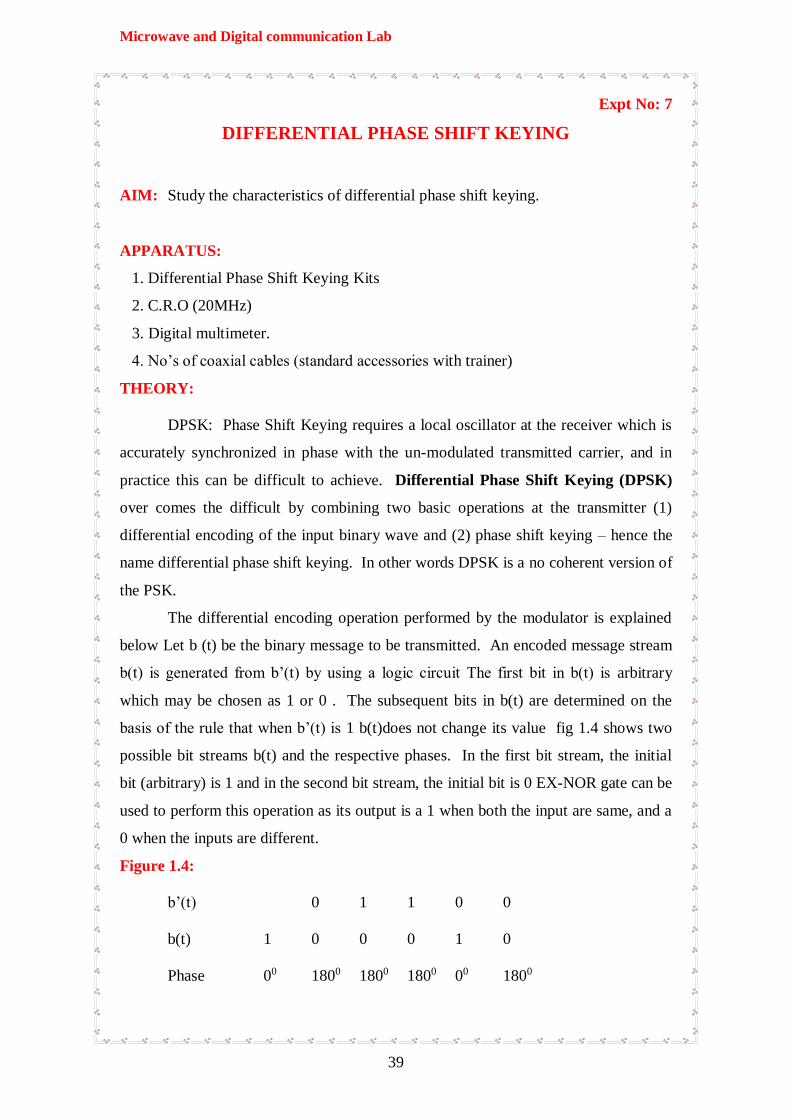
Figure 1.4:
b’(t) 0 1 1 0 0
b(t) 1 0 0 0 1 0
Phase 00 1800 1800 1800 00 1800

Microwave and Digital communication Lab
40
B(t) 0 1 1 1 0 1
Phase 1800 00 00 00 1800 00
Figure 1.5 Example for Complete DPSK operation (with arbitrary bit as 0):
Message signal(to be transmitted) 0 1 1 0 0
Encoded data(differential data) 0 1 1 1 0 1
Transmitted signal phase: 1800 00 00 00 1800 00
Received signal phase : 1800 00 00 00 1800 00
Encoded data(differential data) 0 1 1 1 0
Message signal (Demodulation) 0 1 1 0 0
Dpsk Demodulator:
Fig 1.1 shown the DPSK modulator. This consists of PSK modulator and
differential encoder.
PSK Modulator: IC CD 4052 is a 4 channel analog multiplexer and is used as an
active component in this circuit. One of the control signals of 4052 is grounded so
that 4052 will act as a two channel multiplexer and other control is being connected
to the binary signal i.e., encoded data . Un shifted carrier signal is connected directly
to CH1 and carrier shifted by 1800is connected to CH2. Phase shift network is a unity
gain inverting amplifier using Op-Amp (TL084).
When control signal is at high voltage, output of the 4052 is connected to CH1
and un shifted (or 0 phase) carrier is passed on to output. Similarly when control
signal is at zero voltage output of 4052 is connected to CH2 and carrier shifted by
1800 is passed on to output.
Differential encoder: This consists of 1 bit delay circuit and an X-NOR Gate. 1 bit
delay circuit is formed by a D-Latch. Data signal i.e., signal to be transmitted is
connected to one of the input of the X-NOR gate and other one being connected to out
of the delay circuit. Output of the X-NOR gate and is connected to control input of
the multiplexer (IC 4052) and as well as to input of the D-Latch. Output of the X-
NOR gate is 1 when both the inputs are same and it is 0 when both the inputs are
different.

Microwave and Digital communication Lab
41
Dpsk Demodulator:
Fig 1.2 shows the DPSK Demodulator. This consists of 1 bit delay circuit, X-
NOR Gate and a signal shaping circuit. Signal shaping circuit consists of a Op-amp
based zero crossing detector followed by a D-latch. Receiver DPSK signal is
converted to square wave with the help of zero crossing and this square wave will
pass through the D-Latch. So output of the D-latch is an encoded data. This encoded
data is applied to 1 bit delay circuit as well as to one of the inputs of X-NOR gate.
And output of the delay circuit is connected to another input of the X-NOR gate.
Output of the X-NOR gate is 1 when both the inputs are same and it is 0 when both
the inputs are different.
BLOCK DIAGRAM:
fig (1.1)

Microwave and Digital communication Lab
42
fig(1.2)
PROCEDURE:
Modulation:
1.Connect carrier signal to carrier input of the PSK Modulator.
2.Connect data signal from data input of the X-NOR gate.
3.Keep CRO in dual mode.
4.Connect CH1 input of the CRO to data signal and CH2 input to the encoded data
(which is nothing but the output of the X-NOR gate)
5.Observe the encoded data with respect to data input. The encoded data will be
in a given sequence.
Actual data signal : 10101101001010110100
Encoded data signal : 01100011011001110010
6. Now connect CH2 input of the CRO to the DPSK output and CH1 input to the
encoded data. Observe the input and output waveforms and plot the same.
7. Compare the plotted waveforms with the given waveforms in fig: 1.3
Note: Observe and plot the waveforms after perfect triggering. Better to keep the
encoded data more than 4 cycles for perfect triggering.

Microwave and Digital communication Lab
43
Demodulation:
1. Connect DPSK signal to the input of the signal shaping circuit from DPSK
transmitter with the help of coaxial cable (supplied with trainer).
2. Connect clock from the transmitter ( i.e. DPSK Modulator) to clock input of the
1 bit delay circuit using coaxial cable.
3. Keep CRO in dual mode. Connect CH1 input to the encoded data (at modulator
) and CH2 input to the encoded data ( at demodulator).
4. Observe and plot both the waveforms and compare it with the given waveforms.
You will notice that both the signals are same with one bit delay.
5. Keep CRO in dual mode. Connect CH1 input to the data signal (at modulator)
and CH2 input to the output of the demodulator.
6. Observe and plot both the waveforms and compare it with the given waveforms.
You will notice that both the signals are same with one bit delay.
7. Disconnect clock from transmitter and connect to local oscillator clock (i.e.,
clock generator output from De Modulator) with remaining setup as it is.
Observe demodulator output and compare it with the previous output. This
signal is little bit distorted. This is because lack of synchronization between
clock at modulator and clock at demodulator. You can get further perfection in
output waveform by adjusting the locally generated clock frequency by varying
potentiometer.

Microwave and Digital communication Lab
44
EXPECTEDWAVEFORMS
RESULT:
QUESTIONS:
1. How does DPSK differ from PSK?
2. Explain theoretical modulation & demodulation of DPSK using arbitrary bit
Sequence and assuming initial bit 0 and 1?
3. What is the advantage of DPSK over PSK?
4. Why do we need 1 bit delay in DPSK modulator & demodulator?
5. What does a synchronous detector (multiplier) do in DPSK demodulator?
6. What is the relation between carrier frequency & the bit interval ‘T’?
7. What are the disadvantages of DPSK?
8. Is the error rate of DPSK is greater than PSK?
9. What is the expression for DPSK error?
10. What are the applications of DPSK?

Microwave and Digital communication Lab
45
Expt No: 8
PULSE AMPLITUDE MODULATION & DEMODULATION
AIM: To generate a Pulse amplitude modulated signal and also demodulate the
original signal. APPARATUS:
1. BC107 transistor-1
2. 10KΩ resistors -2
3. Function generators-2
4. CRO
5. Bread board
6. Connecting wires, probes
THEORY:
In pulse Amplitude Modulation the amplitude of the carrier pulses varies in
accordance with the instantaneous values of message signal and the pulse width is
fixed, in practice this is realized by a simple mechanical commutator or by electronic
circuit. Natural PAM signal sampling occurs when finite width is used in the
modulators and tops of the pulses are forced to follow the magnitude of modulating
waveform. Flat tapped PAM system is quite often used because of the generating the
modulating waveform and spectrum. Finite width pulses are used but they are flat
topped after modulation. Reconstruction of original signal is possible by passing the
modulated signal through a low pass filter.
CIRCUIT DIAGRAM:

Microwave and Digital communication Lab
46
PROCEDURE:
1. Connections are made as per the circuit diagram.
2. Modulating signal is given to a collector terminal of a BC 107 transistors and
carrier signal of High frequency is given to a base terminal of a transistor and
switch ON the power supply.
3. Then the modulated output is observed across the transistor emitter terminal.
4. The output characteristics of a PAM signal is plotted on a graph.
OUTPUT WAVEFORM:

Microwave and Digital communication Lab
47
PRECAUTIONS:
1. Connections must be tight.
2. The width of the signal must be noted carefully.
VIVA QUESTIONS:
What are the classifications of pulse modulation techniques?
What is the transmission bandwidth of Pulse amplitude modulation?
What are the Draw backs in Pulse amplitude modulated signal?
What do you mean by synchronization in PAM?
Write the standard equation of a PAM in frequency domain?
What is meant by Aperture effect?
Draw the frequency spectrum of a PAM signal?
What is the time domain representation of a PAM signal?
What are the major differences between PAM &PWM?
Which type of sampling technique is used in PAM signal?
RESULT:
The output characteristic of a Pulse amplitude modulated/demodulated signal
is obtained.

Microwave and Digital communication Lab
48
Expt No: 9
GENERATION AND DETECTION OF QPSK
AIM: To generate QPSK wave and detect it using QPSK module.
APPARATUS:
1. QPSK Modem Kit.
2. Power supply with regulated supply of +5V, + 12V.
3. CRO and CRO Probes.
4. Patch chords and Jumper wires.
THEORY:
QPSK Kit Description
QPSK Transmitter:
XR 2206 generates a master clock of frequency 10 KHz. The clock divider
circuit consists of two numbers of 74HC161. Patch cord is used for selecting data rate
between 600 bps or 300 bps. A 1C 74HC161 form a divide by 8 circuits which is used
for getting a word pulse (WP).CD4014 generates the data. It converts the 8 bit parallel
data in serial form. Data pattern can be selected through the DIP switch SW1. QPSK
system (fig4.1) requires four signals –sin, sin, cos and –cos which are generated using
four number of UA741 through signal processing operation like inversion and
differentiation. 74HC161 and CD 4094 form a two bit shift register used for serial to
parallel conversion (Bit splitter). The two bit parallel output is used for selecting one
of the four signal generated by IC’s UA741. CD14053 and UA741 form a multiplexer
and adder which is used for selecting one of the four signals of the QPSK modulation
depends on the value of two bits of B0 and B1.
QPSK Receiver:
QPSK receiver (fig4.2) consists of band pass filter and two parallel branches
of multiplier, a low pass filter and a comparator. In coming QPSK signal is fed two
parallel branches of multiplier, LPF and level converter. Multiplier is used to remove
the carrier frequency and recover the and band signal. Then it is passed through a LPF
to restrict the noise and made to fall within the base band signal bandwidth. The level
converter is enables the decision circuit to decide ‘1’ or ‘0’ of transmitted bits. The
local carrier is used in the multiplier are sine and cos signal, which ultimately
generates two bit streams B0 and B1 at the output of level converters. These outputs
are then fed to 2 bit parallel to serial bit combiner to recover the original data.

Microwave and Digital communication Lab
49
CIRCUIT DIAGRAM:
QPSK Transmitter
Fig4.1: Block diagram of a QPSK transmitter module.
QPSK Receiver
Fig4.2: Block diagram of a QPSK receiver module

Microwave and Digital communication Lab
50
PROCEDURE:
Transmitter
1. Connect the power supply to the QPSK Kit by using connecter wire +5V, +12
V, -12V (Fig4.1).
2. Select the input bit stream by combination of dip switches here input 8 bits
data is selected. Select the proper transmission rate 600bps or 1200 bps.
3. Select NRZ (L) data at the output of data generator.
4. Measure the clock signal, word pulse and NRZ (L) input data stream.
If transmission rate is 1200 bps then Word pulse width is (1/1200=833 μSec ).
5. Check the odd stream and even stream data output
6. If binary input data 1 1 0 1 1 0 0 0 the odd stream B1= 1 1 0 0 11 00 and
B0= 1 1 1 1 0 0 0 0 as seen in figure
7. The four carrier signal generator with phase is selected according to the
combination of the digits of input data stream (odd and even stream).
8. The output QPSK signal is verified with reference of Word pulse. Here word
pulse is the start of 8 bits input data
Receiver
1. The QPSK modulated signal is fed to the receiver input (fig4.2).
2. Here odd stream B1 offset and even stream B0 offset is used to track the
transmitter odd stream and even stream. So connect transmitter odd stream to
one channel of CRO and receiver odd stream to another channel of CRO, and
check the same bits pattern and repeat same for even stream.
3. Verify the demodulated output with transmitted message signal.
4. The input waveform and expected output waveforms are shown in fig 4.3.
Fig4.3: QPSK output signal with constellation diagram
RESULT: