digital communication using the pic16f84a microcontroller€¦ · the purpose of this project is to...
TRANSCRIPT

DIGITAL COMMUNICATION USING THE PIC16F84A MICROCONTROLLER
Melonee Wise Physics344 Fall 2003
Physics 344 Final Project Fall 2003 Physics Department, University of Illinois Digital Communication By Melonee Wise Instructor: Steve Errede
Page 2/21
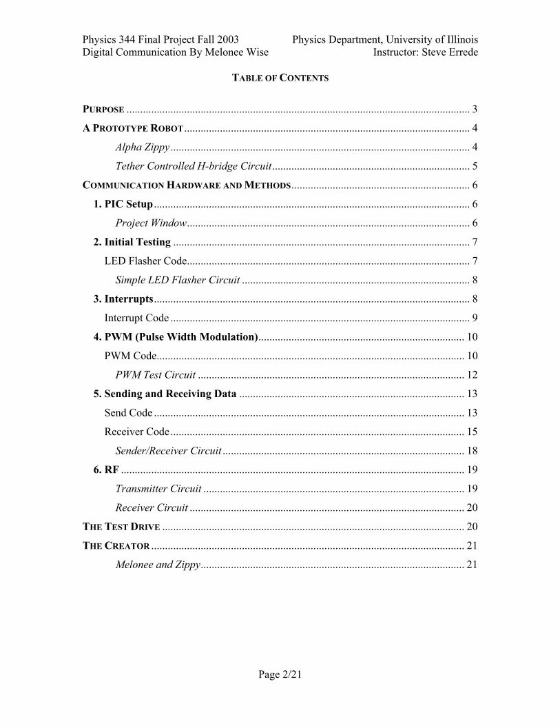
TABLE OF CONTENTS
PURPOSE ............................................................................................................................. 3
A PROTOTYPE ROBOT........................................................................................................ 4
Alpha Zippy ............................................................................................................. 4
Tether Controlled H-bridge Circuit........................................................................ 5
COMMUNICATION HARDWARE AND METHODS................................................................. 6
1. PIC Setup ................................................................................................................... 6
Project Window....................................................................................................... 6
2. Initial Testing ............................................................................................................ 7
LED Flasher Code....................................................................................................... 7
Simple LED Flasher Circuit ................................................................................... 8
3. Interrupts................................................................................................................... 8
Interrupt Code ............................................................................................................. 9
4. PWM (Pulse Width Modulation)........................................................................... 10
PWM Code................................................................................................................ 10
PWM Test Circuit ................................................................................................. 12
5. Sending and Receiving Data .................................................................................. 13
Send Code ................................................................................................................. 13
Receiver Code........................................................................................................... 15
Sender/Receiver Circuit ........................................................................................ 18
6. RF ............................................................................................................................. 19
Transmitter Circuit ............................................................................................... 19
Receiver Circuit .................................................................................................... 20
THE TEST DRIVE .............................................................................................................. 20
THE CREATOR .................................................................................................................. 21
Melonee and Zippy................................................................................................ 21

Physics 344 Final Project Fall 2003 Physics Department, University of Illinois Digital Communication By Melonee Wise Instructor: Steve Errede
Page 3/21
Purpose The purpose of this project is to develop digital communication using the PIC16F84A microcontroller for interface with RF transceivers to control a robot. The specific goals of the project are:
1. Construct Prototype Robot 2. PIC Chip Setup
- Obtain necessary software (MPLAB IDE and PICPRO). - Setup new project within MPLAB. - Configure the assembler code properly for the PIC16F84A chip.
3. Hardware Design - Design necessary test circuitry to test each software progression. - Design necessary circuitry to interface the PIC chips and the RF modules
with the prototype robot. 4. Software Design
- Write a LED flasher program. - Write an interrupt program. - Write a PWM program. - Write a sender program. - Write a receiver program.
5. Test the PIC send and receive protocol. 6. Test the PIC chip with RF. 7. Drive robot around using digital RF controller.

Physics 344 Final Project Fall 2003 Physics Department, University of Illinois Digital Communication By Melonee Wise Instructor: Steve Errede
Page 4/21
A Prototype Robot For this project a prototype robot, Zippy, was built (Figure 1).
Figure 1 Alpha Zippy
Zippy’s main components consist of: 2 pieces of plywood 2 bicycle training wheels 4 bicycle training wheel brackets 2 Pitman motors (donated by the ECE department) 1 12V motorcycle battery 2 pieces of 1 ½ PVC pipe (hold the motors and shafts in place) 2 yards of rope 2 tape holders (counterbalance the battery) 10 or so nuts and bolts 2 H-bridges 1 receiver 1 kill switch
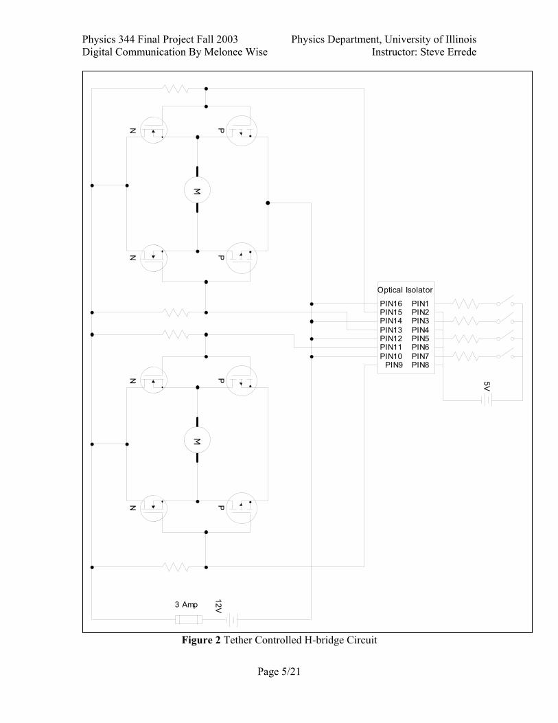
Of the hardware used to construct Zippy only the electrical components will be discussed within this report because it obvious to see the degree of craftsmanship that was necessary to construct the prototype. Initially Zippy was a tether controlled robot, a switch controller was linked directly to the speed controller. The speed controller consisted of two H-bridges that controlled each motor separately. The N-type and P-type mosfets were salvaged off of old computer boards and can handle a max of 6 Amps. A 12V motor cycle battery was used to power the motors and four, slightly used, 1.5V (double A) batteries were used to power the switch logic. A 3 Amp fuse was used on the 12V battery to stop potential hazards (i.e. fires, exploding mosfets, ect.).
Physics 344 Final Project Fall 2003 Physics Department, University of Illinois Digital Communication By Melonee Wise Instructor: Steve Errede
Page 5/21
Figure 2 Tether Controlled H-bridge Circuit
N
M
NN P
M
N P 5V
PIN1PIN2PIN3PIN4PIN5PIN6PIN7PIN8PIN9
PIN10PIN11PIN12PIN13PIN14PIN15PIN16
Optical Isolator
3 Amp
12VP
P
Physics 344 Final Project Fall 2003 Physics Department, University of Illinois Digital Communication By Melonee Wise Instructor: Steve Errede
Page 6/21
Communication Hardware and Methods
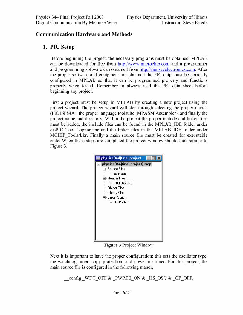
1. PIC Setup Before beginning the project, the necessary programs must be obtained. MPLAB can be downloaded for free from http://www.microchip.com and a programmer and programming software can obtained from http://ramseyelectronics.com. After the proper software and equipment are obtained the PIC chip must be correctly configured in MPLAB so that it can be programmed properly and functions properly when tested. Remember to always read the PIC data sheet before beginning any project. First a project must be setup in MPLAB by creating a new project using the project wizard. The project wizard will step through selecting the proper device (PIC16F84A), the proper language toolsuite (MPASM Assembler), and finally the project name and directory. Within the project the proper include and linker files must be added, the include files can be found in the MPLAB_IDE folder under disPIC_Tools/support/inc and the linker files in the MPLAB_IDE folder under MCHIP_Tools/Lkr. Finally a main source file must be created for executable code. When these steps are completed the project window should look similar to Figure 3.
Figure 3 Project Window
Next it is important to have the proper configuration; this sets the oscillator type, the watchdog timer, copy protection, and power up timer. For this project, the main source file is configured in the following manor,
__config _WDT_OFF & _PWRTE_ON & _HS_OSC & _CP_OFF,
Physics 344 Final Project Fall 2003 Physics Department, University of Illinois Digital Communication By Melonee Wise Instructor: Steve Errede
Page 7/21
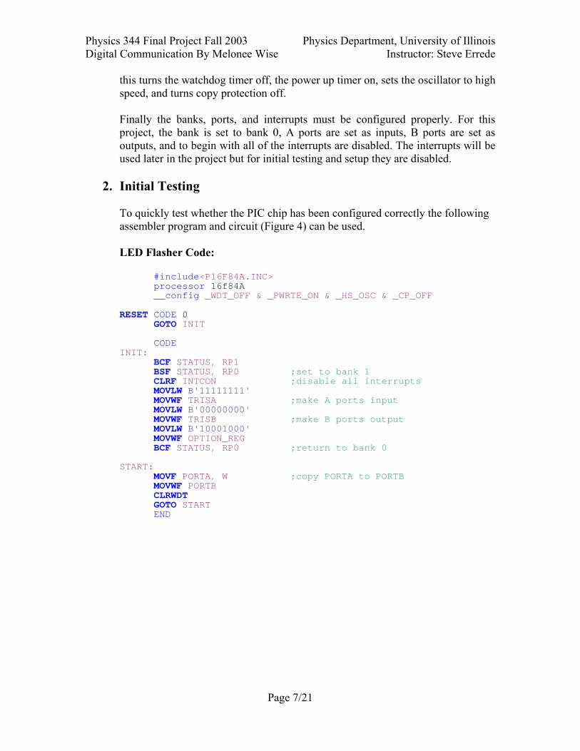
this turns the watchdog timer off, the power up timer on, sets the oscillator to high speed, and turns copy protection off. Finally the banks, ports, and interrupts must be configured properly. For this project, the bank is set to bank 0, A ports are set as inputs, B ports are set as outputs, and to begin with all of the interrupts are disabled. The interrupts will be used later in the project but for initial testing and setup they are disabled.
2. Initial Testing
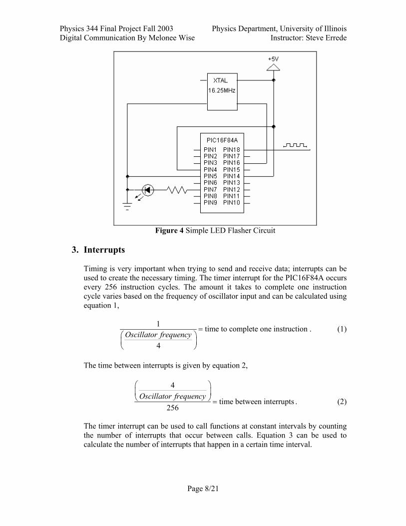
To quickly test whether the PIC chip has been configured correctly the following assembler program and circuit (Figure 4) can be used.
LED Flasher Code:
#include<P16F84A.INC> processor 16f84A __config _WDT_OFF & _PWRTE_ON & _HS_OSC & _CP_OFF RESET CODE 0 GOTO INIT CODE INIT: BCF STATUS, RP1 BSF STATUS, RP0 ;set to bank 1 CLRF INTCON ;disable all interrupts MOVLW B'11111111' MOVWF TRISA ;make A ports input MOVLW B'00000000' MOVWF TRISB ;make B ports output MOVLW B'10001000' MOVWF OPTION_REG BCF STATUS, RP0 ;return to bank 0 START: MOVF PORTA, W ;copy PORTA to PORTB MOVWF PORTB CLRWDT GOTO START END
Physics 344 Final Project Fall 2003 Physics Department, University of Illinois Digital Communication By Melonee Wise Instructor: Steve Errede
Page 8/21
Figure 4 Simple LED Flasher Circuit
3. Interrupts
Timing is very important when trying to send and receive data; interrupts can be used to create the necessary timing. The timer interrupt for the PIC16F84A occurs every 256 instruction cycles. The amount it takes to complete one instruction cycle varies based on the frequency of oscillator input and can be calculated using equation 1,
1 time to complete one instruction 4
Oscillator frequency=
. (1)
The time between interrupts is given by equation 2,
4
time between interrupts256
Oscillator frequency = . (2)
The timer interrupt can be used to call functions at constant intervals by counting the number of interrupts that occur between calls. Equation 3 can be used to calculate the number of interrupts that happen in a certain time interval.
Physics 344 Final Project Fall 2003 Physics Department, University of Illinois Digital Communication By Melonee Wise Instructor: Steve Errede
Page 9/21
4 number of interrupts in x seconds
256
Oscillator frequencytime ⋅ = . (3)
For this project a 16.25MHz clock was used, all calculations are based on this oscillator frequency.
When an interrupt occurs the PCL of the chip is set to register 4 in the memory bank, i.e. the interrupt code must start at 4. When using an interrupt special care must be taken so that the program returns with all of the correct values in the W and STATUS registers. For this project interrupts were used as a timer, each time the interrupt was called it incremented a register which the main program checked. When the registers reached a certain value/time the send or receive function was called to send or receive data. Make sure to use the appropriate number of registers for the amount of time needed, each register can only hold two bits in HEX.
The following interrupt code demonstrates how to store the W and STATUS registers and increment counter registers for timing.
Interrupt Code: #include<P16F84A.INC> processor 16f84A UDATA
W_TEMP res 1 STATUS_TEMP res 1 GLOBAL TIMEC1 TIMEC1 res 1 GLOBAL TIMEC2 TIMEC2 res 1 INTERRUPT CODE 4 ;sets code start to 4th register GOTO PUSH CODE GLOBAL PUSH PUSH: ;save W and status MOVWF W_TEMP SWAPF STATUS, W MOVWF STATUS_TEMP ISR: ;interrupt service routine INCFSZ TIMEC1, F ;if zero increment next register GOTO POP INCF TIMEC2, F ;if zero increment next register POP: ;restore W and status BCF INTCON, T0IF SWAPF STATUS_TEMP, W MOVWF STATUS SWAPF W_TEMP, F SWAPF W_TEMP, W
Physics 344 Final Project Fall 2003 Physics Department, University of Illinois Digital Communication By Melonee Wise Instructor: Steve Errede
Page 10/21
RETFIE ;return from interrupt END
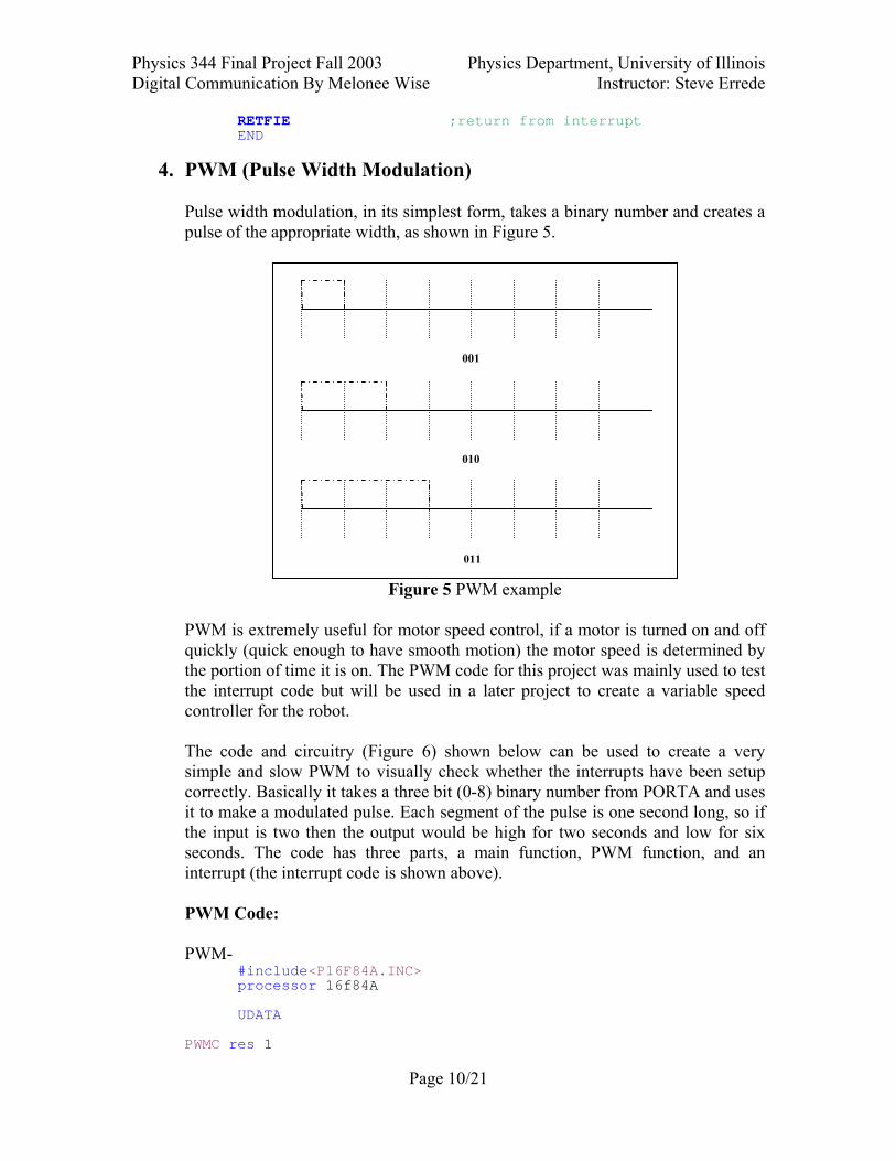
4. PWM (Pulse Width Modulation) Pulse width modulation, in its simplest form, takes a binary number and creates a pulse of the appropriate width, as shown in Figure 5.
Figure 5 PWM example
PWM is extremely useful for motor speed control, if a motor is turned on and off quickly (quick enough to have smooth motion) the motor speed is determined by the portion of time it is on. The PWM code for this project was mainly used to test the interrupt code but will be used in a later project to create a variable speed controller for the robot. The code and circuitry (Figure 6) shown below can be used to create a very simple and slow PWM to visually check whether the interrupts have been setup correctly. Basically it takes a three bit (0-8) binary number from PORTA and uses it to make a modulated pulse. Each segment of the pulse is one second long, so if the input is two then the output would be high for two seconds and low for six seconds. The code has three parts, a main function, PWM function, and an interrupt (the interrupt code is shown above). PWM Code: PWM- #include<P16F84A.INC> processor 16f84A
UDATA PWMC res 1
001
010
011
Physics 344 Final Project Fall 2003 Physics Department, University of Illinois Digital Communication By Melonee Wise Instructor: Steve Errede
Page 11/21
GLOBAL PWM CODE PWM: MOVLW .6 ;decrement or reset counter DECF PWMC, F BTFSC PWMC, 7 MOVWF PWMC ;output the low bits of PORTA onto the low bits of PORTB MOVLW B'00000111' ANDWF PORTA, W IORWF PORTB, F MOVLW B'11111000' IORWF PORTA, W ANDWF PORTB, F MOVFW PORTA ;check count against input value ANDLW B'00000111' SUBWF PWMC, W BTFSS STATUS, C GOTO HIGHOUT GOTO LOWOUT HIGHOUT: ;set bit 6 high BSF PORTB, 6 GOTO NEXT LOWOUT: ;set bit 6 low BCF PORTB, 6 NEXT: RETURN END
MAIN-
#include<P16F84A.INC> processor 16f84A __config _WDT_OFF & _PWRTE_ON & _HS_OSC & _CP_OFF EXTERN TIMEC1 EXTERN TIMEC2 EXTERN PWM RESET CODE 0 GOTO INIT CODE INIT: BCF STATUS, RP1 BSF STATUS, RP0 ;set to bank 1 CLRF INTCON ;disable all interrupts MOVLW B'11111111' MOVWF TRISA ;make A ports input MOVLW B'00000000' MOVWF TRISB ;make B ports output MOVLW B'10001000' MOVWF OPTION_REG BCF STATUS, RP0 ;return to bank 0 MOVLW B'10100000' MOVWF INTCON ;enable timer interrupt START: ;checking to see if has been 1s BCF INTCON, GIE ;stop interrupt while checking time MOVLW H'FD'

Physics 344 Final Project Fall 2003 Physics Department, University of Illinois Digital Communication By Melonee Wise Instructor: Steve Errede
Page 12/21
SUBWF TIMEC1, W BTFSS STATUS, Z GOTO NEXT MOVLW H'3D' SUBWF TIMEC2, W BTFSS STATUS, Z GOTO NEXT MOVLW B'10000000' XORWF PORTB, F CLRF TIMEC1 ;clearing out the timers after 1s CLRF TIMEC2 CALL PWM NEXT: BSF INTCON, GIE ;turning interrupts back on CLRWDT GOTO START END
Figure 6 PWM Test Circuit
Physics 344 Final Project Fall 2003 Physics Department, University of Illinois Digital Communication By Melonee Wise Instructor: Steve Errede
Page 13/21
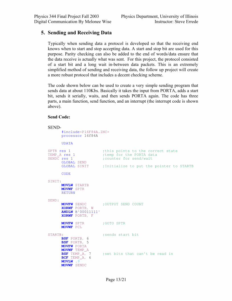
5. Sending and Receiving Data Typically when sending data a protocol is developed so that the receiving end knows when to start and stop accepting data. A start and stop bit are used for this purpose. Parity checking can also be added to the end of words/data ensure that the data receive is actually what was sent. For this project, the protocol consisted of a start bit and a long wait in-between data packets. This is an extremely simplified method of sending and receiving data, the follow up project will create a more robust protocol that includes a decent checking scheme. The code shown below can be used to create a very simple sending program that sends data at about 110Kbs. Basically it takes the input from PORTA, adds a start bit, sends it serially, waits, and then sends PORTA again. The code has three parts, a main function, send function, and an interrupt (the interrupt code is shown above). Send Code: SEND- #include<P16F84A.INC> processor 16f84A UDATA SPTR res 1 ;this points to the correct state TEMP_A res 1 ;temp for the PORTA data SENDC res 1 ;counter for send/wait GLOBAL SEND GLOBAL SINIT ;Initialize to put the pointer to STARTB CODE SINIT: MOVLW STARTB MOVWF SPTR RETURN SEND: MOVFW SENDC ;OUTPUT SEND COUNT XORWF PORTB, W ANDLW B'00011111' XORWF PORTB, F MOVFW SPTR ;GOTO SPTR MOVWF PCL STARTB: ;sends start bit BSF PORTB, 6 BSF PORTB, 5 MOVFW PORTA MOVWF TEMP_A BSF TEMP_A, 7 ;set bits that can’t be read in BCF TEMP_A, 6 MOVLW .9 MOVWF SENDC

Physics 344 Final Project Fall 2003 Physics Department, University of Illinois Digital Communication By Melonee Wise Instructor: Steve Errede
Page 14/21
NEXTB: ;figures out next bit to output MOVLW ONEOUT BTFSS TEMP_A, 0 MOVLW ZEROOUT MOVWF SPTR ;sets the pointer to the right output RRF TEMP_A, F DECFSZ SENDC, F RETURN MOVLW SENDW ;if done sending go wait for awhile MOVWF SPTR MOVLW .9 ;wait a little bit before resending data MOVWF SENDC RETURN ONEOUT: ;output high BCF PORTB, 5 BSF PORTB, 6 GOTO NEXTB ;go figure out next bit ZEROOUT: ;output low BCF PORTB, 5 BCF PORTB, 6 GOTO NEXTB ;go figure out next bit SENDW: BCF PORTB, 6 ;go low while waiting DECFSZ SENDC, F RETURN MOVLW STARTB MOVWF SPTR RETURN END
MAIN-
#include<P16F84A.INC> processor 16f84A __config _WDT_OFF & _PWRTE_ON & _HS_OSC & _CP_OFF EXTERN TIMEC1 EXTERN TIMEC2 EXTERN SEND EXTERN SINIT RESET CODE 0 GOTO INIT CODE INIT: BCF STATUS, RP1 BSF STATUS, RP0 ;set to bank 1 CLRF INTCON ;disable all interrupts MOVLW B'11111111' MOVWF TRISA ;make A ports input MOVLW B'00000000' MOVWF TRISB ;make B ports output MOVLW B'10001000' MOVWF OPTION_REG BCF STATUS, RP0 ;return to bank 0 CALL SINIT
MOVLW B'10100000' MOVWF INTCON ;enable timer interrupt START: ;checking to see if has been .009s
Physics 344 Final Project Fall 2003 Physics Department, University of Illinois Digital Communication By Melonee Wise Instructor: Steve Errede
Page 15/21
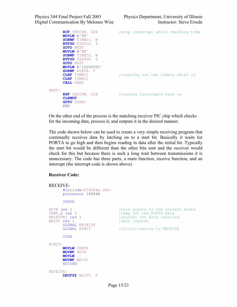
BCF INTCON, GIE ;stop interrupt while checking time MOVLW H'90' SUBWF TIMEC1, W BTFSS STATUS, Z GOTO NEXT MOVLW H'00' SUBWF TIMEC2, W BTFSS STATUS, Z GOTO NEXT MOVLW B'10000000' XORWF PORTB, F CLRF TIMEC1 ;clearing out the timers after 1s CLRF TIMEC2 CALL SEND NEXT: BSF INTCON, GIE ;turning interrupts back on CLRWDT GOTO START END On the other end of the process is the matching receiver PIC chip which checks for the incoming data, process it, and outputs it in the desired manner. The code shown below can be used to create a very simple receiving program that continually receives data by latching on to a start bit. Basically it waits for PORTA to go high and then begins reading in data after the initial bit. Typically the start bit would be different than the other bits sent and the receiver would check for this but because there is such a long wait between transmissions it is unnecessary. The code has three parts, a main function, receive function, and an interrupt (the interrupt code is shown above). Receiver Code: RECEIVE- #include<P16F84A.INC> processor 16f84A UDATA RPTR res 1 ;this points to the correct state TEMP_B res 1 ;temp for the PORTA data RECEIVEC res 1 ;counter for bits received WAITC res 1 ;wait counter GLOBAL RECEIVE GLOBAL RINIT ;Initialization to RECEIVE CODE RINIT: MOVLW CHECK MOVWF RPTR MOVLW .1 MOVWF WAITC RETURN RECEIVE: DECFSZ WAITC, F

Physics 344 Final Project Fall 2003 Physics Department, University of Illinois Digital Communication By Melonee Wise Instructor: Steve Errede
Page 16/21
RETURN MOVFW RPTR ;GOTO RPTR MOVWF PCL
CHECK: ;runs receive when line goes high MOVLW .1 MOVWF WAITC BTFSS PORTA, 0 RETURN STARTB: ;sees start bit MOVLW .8 MOVWF RECEIVEC ;number of bits to read in MOVLW .9 ;wait until middle of bit0 MOVWF WAITC MOVLW READIN ;set wait state MOVWF RPTR BSF PORTA, 2 BSF PORTA, 3 RETURN READIN: BCF PORTA, 3 MOVLW B'00000100' XORWF PORTA, F RRF TEMP_B, F ;read in new bit BSF TEMP_B, 7 BTFSS PORTA, 0 BCF TEMP_B, 7 MOVLW .6 ;wait for new bit MOVWF WAITC DECFSZ RECEIVEC, F ;check to see if 8 bits were read RETURN BCF PORTA, 2 MOVFW TEMP_B ;finished receiving one byte ;wait MOVWF PORTB MOVLW .12 ;wait for next start MOVWF WAITC MOVLW CHECK MOVWF RPTR RETURN END MAIN-
#include<P16F84A.INC> processor 16f84A __config _WDT_OFF & _PWRTE_ON & _HS_OSC & _CP_OFF EXTERN TIMEC1 EXTERN TIMEC2 EXTERN RECEIVE EXTERN RINIT RESET CODE 0 GOTO INIT CODE INIT: BCF STATUS, RP1 BSF STATUS, RP0 ;set to bank 1 CLRF INTCON ;disable all interrupts MOVLW B'11111111'

Physics 344 Final Project Fall 2003 Physics Department, University of Illinois Digital Communication By Melonee Wise Instructor: Steve Errede
Page 17/21
MOVWF TRISA ;make A ports input MOVLW B'00000000' MOVWF TRISB ;make B ports output MOVLW B'10001000' MOVWF OPTION_REG BCF STATUS, RP0 ;return to bank 0 CALL RINIT
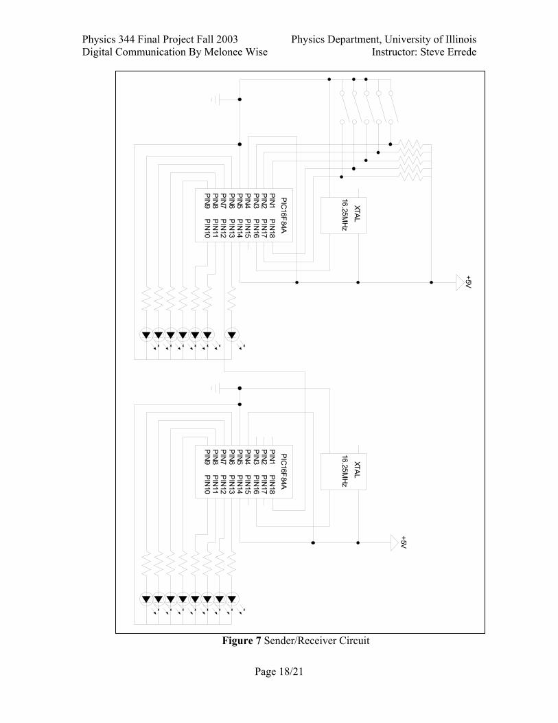
MOVLW B'10100000' MOVWF INTCON ;enable timer interrupt START: ;checking to see if has been .0015s BCF INTCON, GIE ;stop interrupt while checking time MOVLW H'18' SUBWF TIMEC1, W BTFSS STATUS, Z GOTO NEXT MOVLW H'00' SUBWF TIMEC2, W BTFSS STATUS, Z GOTO NEXT MOVLW B'10000000' XORWF PORTB, F CLRF TIMEC1 ;clearing out the timers after 1s CLRF TIMEC2 CALL RECEIVE NEXT: BSF INTCON, GIE ;turning interrupts back on CLRWDT GOTO START END Once both chips have been properly programmed the following test circuitry (Figure 7) can be used. The switches on the first chip control the input into PORTA 0-5 and the data is output on PORTB 6. The second chip reads the data in on PORT A 0 and outputs it to the LEDs using PORTB.
Physics 344 Final Project Fall 2003 Physics Department, University of Illinois Digital Communication By Melonee Wise Instructor: Steve Errede
Page 18/21
Figure 7 Sender/Receiver Circuit
PIN1PIN2PIN3PIN4PIN5PIN6PIN7PIN8PIN9
PIN10
PIN11
PIN12
PIN13
PIN14
PIN15
PIN16
PIN17
PIN18
PIC16F84A
XTAL
16.25MHz
+5V
PIN1PIN2PIN3PIN4PIN5PIN6PIN7PIN8PIN9
PIN10PIN11PIN12PIN13PIN14PIN15PIN16PIN17PIN18
PIC16F84A
XTAL
16.25MH
z
+5V
Physics 344 Final Project Fall 2003 Physics Department, University of Illinois Digital Communication By Melonee Wise Instructor: Steve Errede
Page 19/21
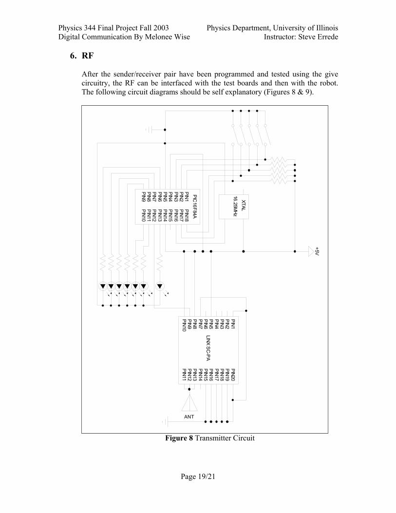
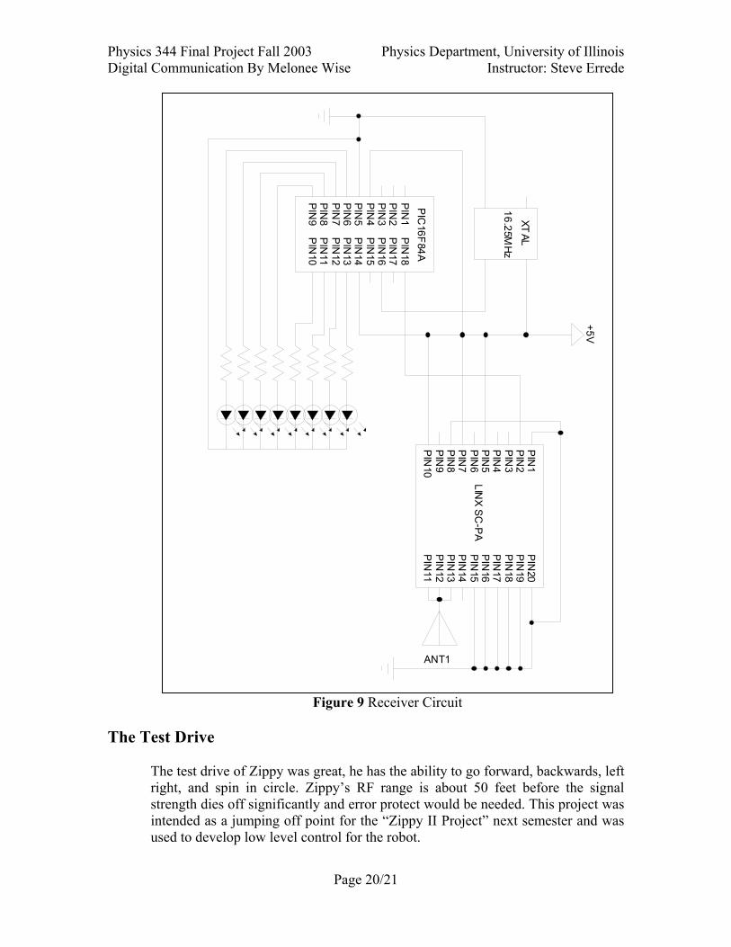
6. RF
After the sender/receiver pair have been programmed and tested using the give circuitry, the RF can be interfaced with the test boards and then with the robot. The following circuit diagrams should be self explanatory (Figures 8 & 9).
Figure 8 Transmitter Circuit
PIN1
PIN2
PIN3
PIN4
PIN5
PIN6
PIN7
PIN8
PIN9
PIN10
PIN11
PIN12
PIN13
PIN14
PIN15
PIN16
PIN17
PIN18
PIC16F84A
XTAL
16.25MH
z
+5V
PIN1
PIN2
PIN3
PIN4
PIN5
PIN6
PIN7
PIN8
PIN9
PIN10
PIN11
PIN12
PIN13
PIN14
PIN15
PIN16
PIN17
PIN18
PIN19
PIN20
LINX SC-PA
ANT
Physics 344 Final Project Fall 2003 Physics Department, University of Illinois Digital Communication By Melonee Wise Instructor: Steve Errede
Page 20/21
Figure 9 Receiver Circuit
The Test Drive
The test drive of Zippy was great, he has the ability to go forward, backwards, left right, and spin in circle. Zippy’s RF range is about 50 feet before the signal strength dies off significantly and error protect would be needed. This project was intended as a jumping off point for the “Zippy II Project” next semester and was used to develop low level control for the robot.
PIN1
PIN2
PIN3
PIN4
PIN5
PIN6
PIN7
PIN8
PIN9
PIN10
PIN11
PIN12
PIN13
PIN14
PIN15
PIN16
PIN17
PIN18
PIC
16F84A
XTAL
16.25MH
z
+5V
ANT1
PIN1
PIN2
PIN3
PIN4
PIN5
PIN6
PIN7
PIN8
PIN9
PIN10
PIN11
PIN12
PIN13
PIN14
PIN15
PIN16
PIN17
PIN18
PIN19
PIN20
LINX SC
-PA
Physics 344 Final Project Fall 2003 Physics Department, University of Illinois Digital Communication By Melonee Wise Instructor: Steve Errede
Page 21/21
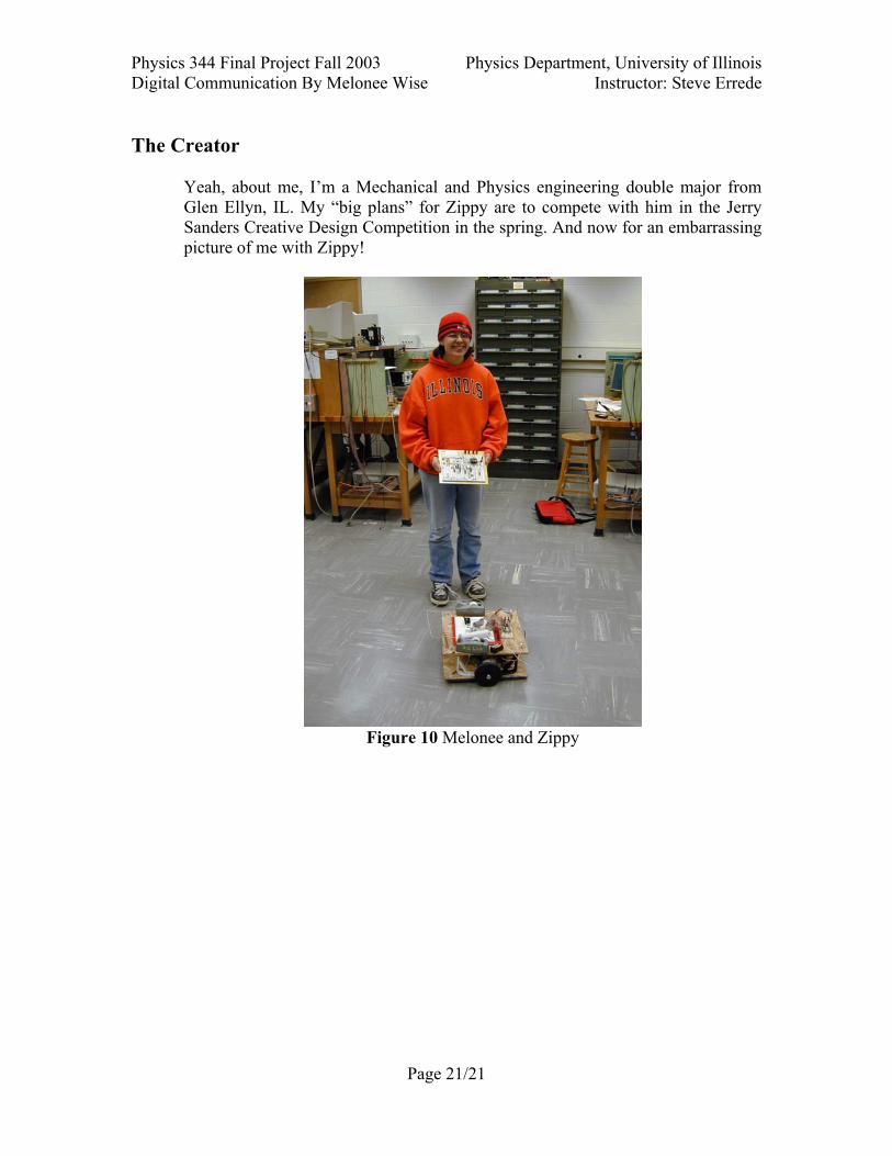
The Creator
Yeah, about me, I’m a Mechanical and Physics engineering double major from Glen Ellyn, IL. My “big plans” for Zippy are to compete with him in the Jerry Sanders Creative Design Competition in the spring. And now for an embarrassing picture of me with Zippy!
Figure 10 Melonee and Zippy