digital combinational logic part-ii
TRANSCRIPT
7/31/2019 Digital Combinational Logic Part-II
http://slidepdf.com/reader/full/digital-combinational-logic-part-ii 1/4
6/27/12 Digital Combinational Logic Part-II
1/4www.asic-world.com/digital/combo2.html
Digital Combinational Logic
Part-IIFeb-15-2012
Enter tutorial you want
to buy
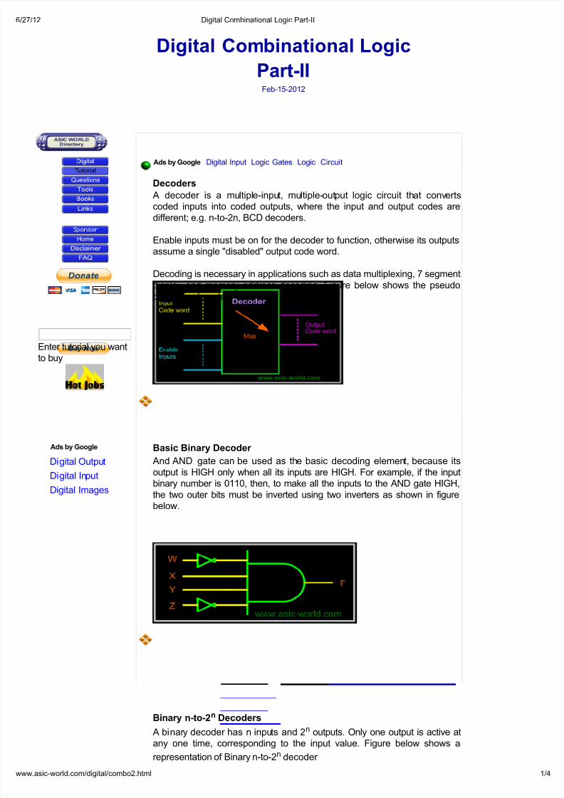
Decoders
A decoder is a multiple-input, multiple-output logic circuit that converts
coded inputs into coded outputs, where the input and output codes are
different; e.g. n-to-2n, BCD decoders.
Enable inputs must be on for the decoder to function, otherwise its outputs
assume a single "disabled" output code word.
Decoding is necessary in applications such as data multiplexing, 7 segment
display and memory address decoding. Figure below shows the pseudo
block of a decoder.
Basic Binary Decoder
And AND gate can be used as the basic decoding element, because its
output is HIGH only when all its inputs are HIGH. For example, if the input
binary number is 0110, then, to make all the inputs to the AND gate HIGH,
the two outer bits must be inverted using two inverters as shown in figure
below.
Binary n-to-2n Decoders
A binary decoder has n inputs and 2n outputs. Only one output is active at
any one time, corresponding to the input value. Figure below shows a
representation of Binary n-to-2n decoder
Ads by Google
Digital Output
Digital Input
Digital Images
Ads by Google Digital Input Logic Gates Logic Circuit

7/31/2019 Digital Combinational Logic Part-II
http://slidepdf.com/reader/full/digital-combinational-logic-part-ii 2/4
6/27/12 Digital Combinational Logic Part-II
2/4www.asic-world.com/digital/combo2.html
Example - 2-to-4 Binary Decoder
A 2 to 4 decoder consists of two inputs and four outputs, truth table and
symbols of which is shown below.
Truth Table
X Y F0 F1 F2 F3
0 0 1 0 0 00 1 0 1 0 0
1 0 0 0 1 0
1 1 0 0 0 1
Symbol
To minimize the above truth table we may use kmap, but doing that you will
realize that it is a waste of time. One can directly write down the function for
each of the outputs. Thus we can draw the circuit as shown in figure below.
Note: Each output is a 2-variable minterm (X'Y', X'Y, XY', XY)
Circuit
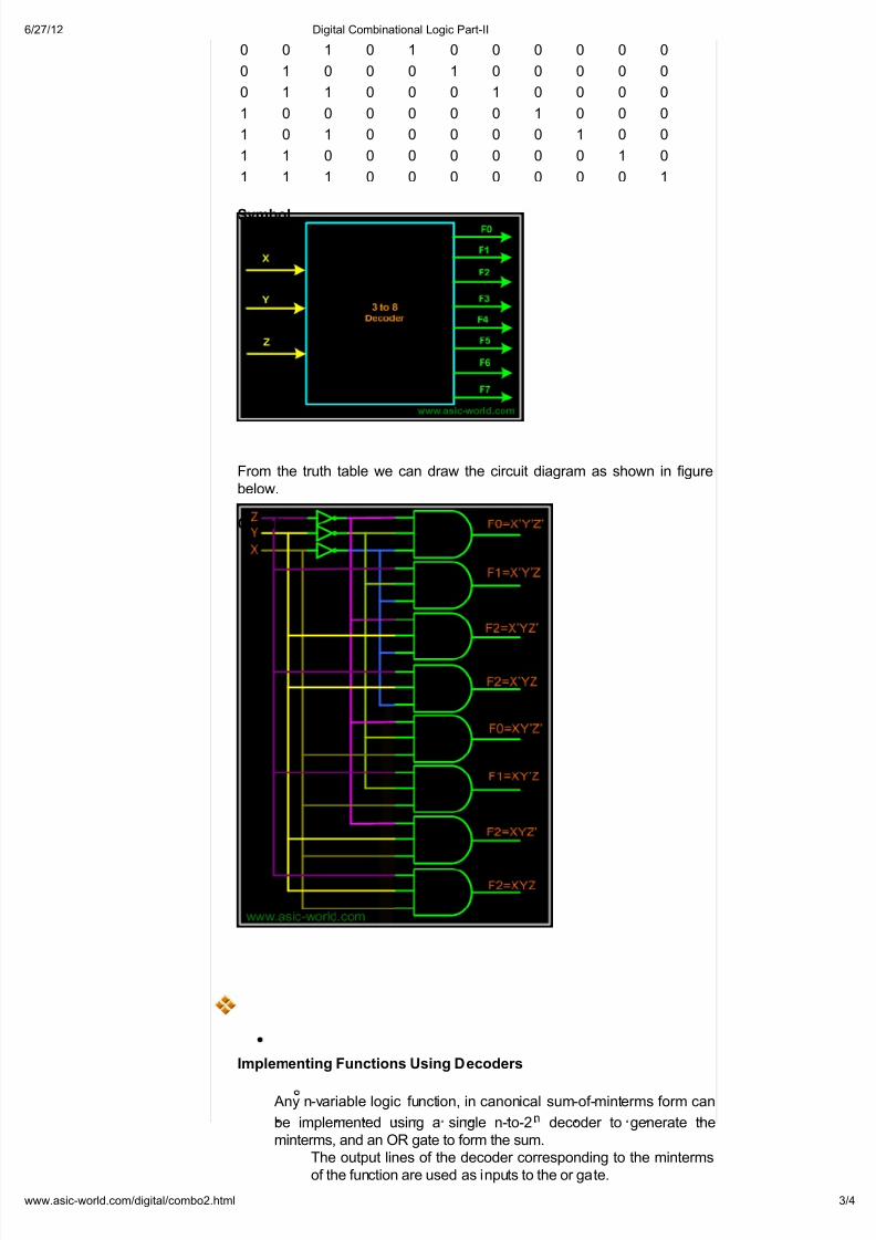
Example - 3-to-8 Binary Decoder
A 3 to 8 decoder consists of three inputs and eight outputs, truth table andsymbols of which is shown below.
Truth Table
X Y Z F0 F1 F2 F3 F4 F5 F6 F7
0 0 0 1 0 0 0 0 0 0 0
7/31/2019 Digital Combinational Logic Part-II
http://slidepdf.com/reader/full/digital-combinational-logic-part-ii 3/4
6/27/12 Digital Combinational Logic Part-II
3/4www.asic-world.com/digital/combo2.html
0 0 1 0 1 0 0 0 0 0 0
0 1 0 0 0 1 0 0 0 0 0
0 1 1 0 0 0 1 0 0 0 0
1 0 0 0 0 0 0 1 0 0 0
1 0 1 0 0 0 0 0 1 0 0
1 1 0 0 0 0 0 0 0 1 0
1 1 1 0 0 0 0 0 0 0 1
Symbol
From the truth table we can draw the circuit diagram as shown in figure
below.
Circuit
Implementing Functions Using Decoders
Any n-variable logic function, in canonical sum-of-minterms form can
be implemented using a single n-to-2n decoder to generate the
minterms, and an OR gate to form the sum.
The output lines of the decoder corresponding to the minterms
of the function are used as inputs to the or gate.
7/31/2019 Digital Combinational Logic Part-II
http://slidepdf.com/reader/full/digital-combinational-logic-part-ii 4/4
6/27/12 Digital Combinational Logic Part-II
4/4www.asic-world.com/digital/combo2.html
ny com na ona c rcu w n npus an m oupus can e
implemented with an n-to-2n decoder with m OR gates.
Suitable when a circuit has many outputs, and each output function is
expressed with few minterms.
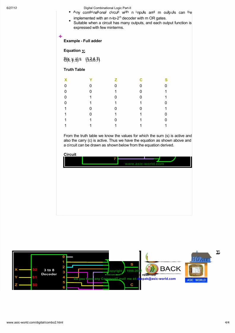
Example - Full adder
Equation
S(x, y, z) = (1,2,4,7)C(x, y, z) = (3,5,6,7)
Truth Table
X Y Z C S
0 0 0 0 0
0 0 1 0 1
0 1 0 0 1
0 1 1 1 0
1 0 0 0 1
1 0 1 1 0
1 1 0 1 0
1 1 1 1 1
From the truth table we know the values for which the sum (s) is active and
also the carry (c) is active. Thus we have the equation as shown above and
a circuit can be drawn as shown below from the equation derived.
Circuit
Copyright © 1998-2012
Deepak Kumar Tala - All rights reserved
Do you have any Comment? mail me at:[email protected]