digital circuits - dalhousie university · pdf filebinary numbers ... multilevel combinational...
TRANSCRIPT

1
ECED2200 Digital Circuits Notes – © 2012 Dalhousie University
Digital Circuits
Electrical & Computer Engineering Department (ECED) Course Notes
ECED2200

2
ECED2200 Digital Circuits Notes – © 2012 Dalhousie University
Table of Contents Digital Circuits ............................................................................................................................................... 7
Logic Gates ......................................................................................................... 8
AND Gate ....................................................................................................... 8
OR Gate .......................................................................................................... 9
NOT Gate ..................................................................................................... 10
NOR Gate ..................................................................................................... 11
NAND Gates ................................................................................................. 12
XOR Gate ...................................................................................................... 15
X NOR Gate .................................................................................................. 16
Additional Gates........................................................................................... 17
Electric Switches ...............................................................................................17
Diodes .......................................................................................................... 17
Transistors ................................................................................................... 19
Logic Classifications ..........................................................................................21
The Breadboard ................................................................................................23
Number Systems ......................................................................................................................................... 25
Binary Numbers ........................................................................................... 25
Number Conversion ..........................................................................................26
Binary to Decimal Conversion ...................................................................... 26
Decimal to Binary Conversion ...................................................................... 27
Binary Arithmetic ..............................................................................................28
Binary Addition ............................................................................................ 28
Binary Subtraction........................................................................................ 30
Binary Multiplication .................................................................................... 31
Binary Division ............................................................................................. 33

3
ECED2200 Digital Circuits Notes – © 2012 Dalhousie University
Bits, Bytes and Words .......................................................................................35
Other Notations ................................................................................................35
Octal Number System .................................................................................. 35
Hexadecimal Numbering System .................................................................. 37
Signed Magnitudes ...........................................................................................39
Complements ............................................................................................... 40
Two’s Complement Arithmetic ..................................................................... 44
Binary Coded Decimal .......................................................................................47
Boolean Algebra .......................................................................................................................................... 48
Boolean Theorems ....................................................................................... 48
Boolean Postulates in 0 and 1 ...................................................................... 48
Basic Boolean Identities ............................................................................... 49
De Morgan’s Theorems ................................................................................ 51
Logic Circuit Analysis .................................................................................... 52
Two-Level Combinational Logic .........................................................................54
Logic Circuit Synthesis ................................................................................................................................. 55
Adding ..............................................................................................................55
The Half Adder ............................................................................................. 55
The Full Adder .............................................................................................. 58
Subtraction .......................................................................................................63
Direct Approach ........................................................................................... 63
Indirect Approach (Using Adders) ................................................................ 64
Arithmetic Logic Unit (ALU) ...............................................................................64
A Design Procedure ...........................................................................................65
Two-Level Canonical Forms ........................................................................................................................ 69
Sum of Products ........................................................................................... 69
Product of Sums ........................................................................................... 72

4
ECED2200 Digital Circuits Notes – © 2012 Dalhousie University
Conversion Between Canonical Forms ......................................................... 72
Positive Versus Negative Logic ..................................................................... 74
Minimization by Mapping ........................................................................................................................... 76
Karnaugh Maps (K-Maps) ............................................................................. 76
Mapping in Four Variables ........................................................................... 83
Five-Variable Maps....................................................................................... 87
Comments on Maps ..................................................................................... 89
Some More Notes: Implicants ...................................................................... 94
Multilevel Combinational Logic ................................................................................................................ 100
Conversion to NAND and NOR Networks ................................................................................................. 102
Computer Aided Design Tools................................................................................................................... 108
Time Response in Combination Networks ................................................................................................ 109
Gate Delays ................................................................................................ 109
Timing Waveforms ..................................................................................... 109
Hazards and Glitches ................................................................................................................................. 111
Hazards in Multilevel Networks ................................................................. 115
Programmable and Steering Logic ............................................................................................................ 120
PAL’s and PLA’s .......................................................................................... 120
The Difference Between PLA’s and PAL’s ................................................... 121
Design Procedure ....................................................................................... 127
Beyond Simple Logic Gates ....................................................................................................................... 133
Switching Logic ............................................................................................... 133
Multiplexer/Data Selector............................................................................... 133
Multiplexer as a Logic Building Block .............................................................. 137
Decoders/Demultiplexer/Data Distribution .................................................... 140
Decoder/Demultiplexer as a Logic Building Block ....................................... 142
Tri-State Gates ................................................................................................ 145
Sequential Logic Design ............................................................................................................................ 147

5
ECED2200 Digital Circuits Notes – © 2012 Dalhousie University
Logic Gate Memory Units................................................................................ 147
Inverter Chains ........................................................................................... 147
Cross-Coupled NOR Gates .......................................................................... 148
Timing Waveforms ..................................................................................... 152
The Data Latch ........................................................................................... 153
The D Flip-Flops .......................................................................................... 155
Timing ........................................................................................................ 156
The JK-Flip Flop .......................................................................................... 157
The T Flip-Flop ............................................................................................ 161
Conversion of One Flip-Flop Type to Another ............................................ 162
Practical Matters ............................................................................................. 168
Debouncing Switches ................................................................................. 169
The 555 Timer ............................................................................................ 170
Sequential Logic Applications .......................................................................... 172
Registers .................................................................................................... 172
Shift Registers ............................................................................................ 172
A Practical Register ......................................................................................... 175
Counters .................................................................................................................................................... 176
Types of Counters ........................................................................................... 176
Divide-by-n Circuits .................................................................................... 176
Binary Ripple Counter ................................................................................ 177
Decade Counters ........................................................................................ 180
Synchronous Counters ............................................................................... 183
Ring Counters ............................................................................................. 184
Counter Design Procedure .............................................................................. 185
Self-Starting Counters ..................................................................................... 191

6
ECED2200 Digital Circuits Notes – © 2012 Dalhousie University
Verifying if a Counter is Self-Starting .......................................................... 191
Counter Reset ............................................................................................ 193
Implementation with Different Kinds of Flip-Flops .......................................... 194
Comparison & Summary of Different Implementations ............................. 204
Memory ..................................................................................................................................................... 207
RAM ........................................................................................................... 207
ROM ........................................................................................................... 211
Finite State Machines................................................................................................................................ 216
Finite State Machine Design Procedure .......................................................... 216
Moore and Mealy Machines ........................................................................... 227
The Moor Machine ..................................................................................... 227
The Mealy Machine .................................................................................... 229
Alternative State Machine Representations ............................................... 236

7
ECED2200 Digital Circuits Notes – © 2012 Dalhousie University
Digital Circuits Digital Circuits have inputs and outputs that are represented by discrete values. The figure below shows a typical output for a digital circuit.
There are two possible output values, namely ±5 volts. Two distinct voltage levels separated by a forbidden region electronically represent the binary numbers 1 and 0.

8
ECED2200 Digital Circuits Notes – © 2012 Dalhousie University
In analog circuits the inputs and outputs have continuous values as show below:
Analog waveform more realistically represent physical quantities such as sound and temperature. Digital waveforms only approximate real values if there are many discrete values. Digital waveforms, however, can best represent degraded signals.
Logic Gates A gate is a device that controls the flow of information, usually in the form
of pulses. Each logic operation will be indicated by a symbol whose function is defined by a truth table that shows all possible inputs and the corresponding outputs.
AND Gate
Symbol
A ● B is read “A and B”.

9
ECED2200 Digital Circuits Notes – © 2012 Dalhousie University
Truth Table
An output appears only when there are inputs at A and B. In general, there may be several input terminals.
Typical Response A typical response for two inputs varying with time is shown below:
OR Gate
Symbol
10
ECED2200 Digital Circuits Notes – © 2012 Dalhousie University
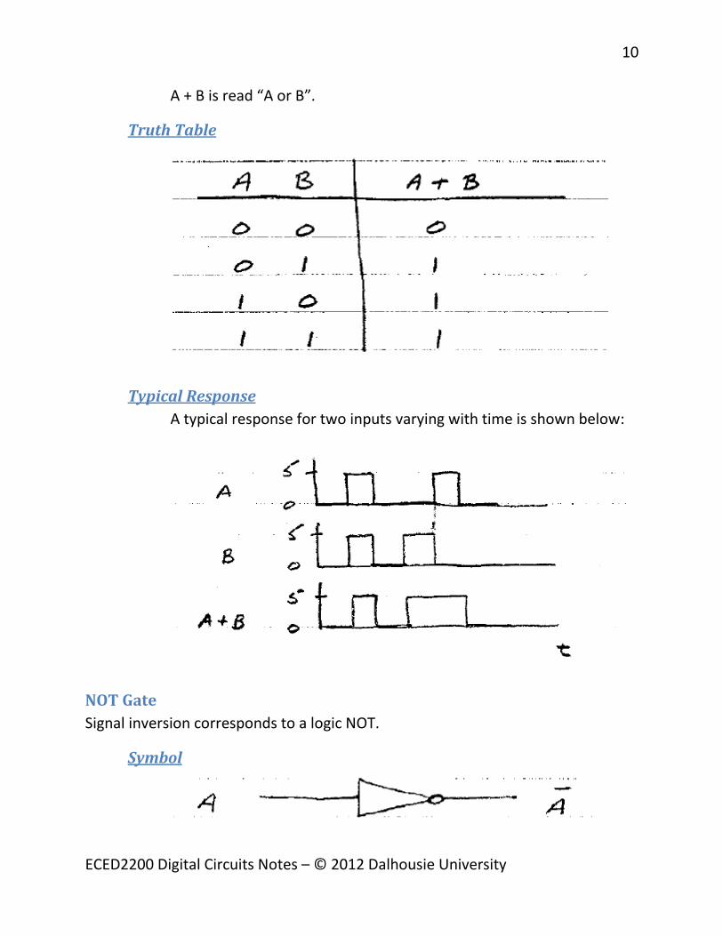
A + B is read “A or B”.
Truth Table
Typical Response A typical response for two inputs varying with time is shown below:
NOT Gate Signal inversion corresponds to a logic NOT.
Symbol

11
ECED2200 Digital Circuits Notes – © 2012 Dalhousie University
A is read “not A”.
Truth Table
The NOT element is an inverter; the output is the complement of the signal input.
Typical Response
NOR Gate An inverted OR gate results in a NOT OR or NOR operation.
Symbol

12
ECED2200 Digital Circuits Notes – © 2012 Dalhousie University
The small circle at the output of the gate, and the line over A + B indicate the inversion process. Thus A+B is A+B inverted.
Truth Table
Typical Response
All basic logic operations can be achieved by using only NOR gates.
NAND Gates An inverted AND gate results in a NOT AND or NAND operation. A NAND gate has all the advantages of a NOR gate and is very easy to fabricate. In a complex logic system, it is convenient to use one type of gate, even when simpler types would be satisfactory, so that gate characteristics are the same for the whole system.

13
ECED2200 Digital Circuits Notes – © 2012 Dalhousie University
Symbol
The small circle and the line over A ● B indicate inversion.
Truth Table
Typical Response

14
ECED2200 Digital Circuits Notes – © 2012 Dalhousie University
Three NAND gates can be used to replace an OR gate. The combination of NAND gates is equivalent to an OR gate in that it performs the same logic operation (see example below).
Example: Use NAND gates to form a two-input OR gate.
The desired function is defined by the following truth table:
From the table we see that if each input were inverted (replaced by its complement) the NAND gate would produce the desired result as indicated in the table.
To obtain the inversion, tie both terminals of a NAND gate together as shown below.
In digital notation, the function f is defined by:

15
ECED2200 Digital Circuits Notes – © 2012 Dalhousie University
A•B A+Bf = =
This relation was obtained by comparing the desired and available truth tables. A “digital algebra” for direct manipulation of such expressions will be considered later.
XOR Gate As indicated by the truth tables, the Exclusive-OR operation can be expressed as (A+B) • (A•B)which reads “(A or B) and not (A and B)”. The alternate formA•B + A•B is called an inequality comparator since it provides an output of one if A and B are not equal.
Symbol
Truth Table
One realization of this gate is shown below:

16
ECED2200 Digital Circuits Notes – © 2012 Dalhousie University
X NOR Gate The exclusive-NOR operator can be expressed as (see the truth tables) A•B+A•B .
It is the inverse of the inequality comparator A•B + A•B . This is an “equality comparator” since the output is 1 if A and B are equal.
Symbol
Truth Table
One realization of this gate is shown below:

17
ECED2200 Digital Circuits Notes – © 2012 Dalhousie University
Additional Gates The following truth table shows all possible gates. This is based on writing out all possible variations of the truth table, with names for some of those gates given:
Electric Switches
Diodes A diode is a two-terminal electrical device that allows current to flow in one direction but not the other. A schematic diagram from a diode is shown below.

18
ECED2200 Digital Circuits Notes – © 2012 Dalhousie University
If the anode is at a higher voltage than the cathode, the diode is forward biased, its resistance is very low, and current flows. The diode has voltage drop of about 0.7V across it. If the anode is at a lower voltage than the cathode, the diode is reverse biased, its resistance is very high, and no current flows.
Simple gates can be constructed by using diodes and a resistor. An AND gate is shown below:
If the inputs are positive (> +5V) with respect to ground, inputs at A and B turn off both diodes, no current flows through R and there is a positive output (a 1). In general, there may be several input terminals. If any of those inputs are zero (0), current flows through the forward-biased diode, and the output is nearly zero (0).
An OR gate is shown below:

19
ECED2200 Digital Circuits Notes – © 2012 Dalhousie University
For no input (zero voltage) no current flows and the output is zero (0). An input of +5V (1) at either terminal A or B on both (or on any terminal in the general case) forward biases the corresponding diode, current flows through the resistor, and the output voltage rises to nearly 5V (1).
The voltage drop across the diodes add up when circuits of this type are cascaded in series and the voltage levels are degraded. Note that it is not possible to construct and inverter using only diodes and resistors. Transistors can be used to circumvent these problems.
Transistors
Bipolar A bipolar transistor is a three-terminal semiconductor device. Under control of one of the terminals, called the base, current can below from the collector terminal to the emitter terminal.
The basic inverter circuit is shown below.

20
ECED2200 Digital Circuits Notes – © 2012 Dalhousie University
A high voltage at the base turns on the transistor. The output f is discharged to ground, getting close to 0V (but never quite reaching it). When a low voltage is placed on the base, the transistor is turned off. The output node f voltage approaches the power supply voltage Vcc through the pull-up/load resistor R1.
Metal Oxide Semiconductor A Metal Oxide Semiconductor (MOS) transistor is a voltage-controlled switch. It has three terminals: a source, a drain, and a gate. There are two different types of MOS transistors, called nmos and pmos. Their schematic symbols are shown below:
An nmos transistor conducts when a high voltage (1) is placed on its gate, and is non-conducting when a zero voltage (0) is on the gate. The pmos transistor is complementary. A pmos transistor conducts when a logic 0 is placed on the gate, and is non-conducting when a logic 1 is on the gate.

21
ECED2200 Digital Circuits Notes – © 2012 Dalhousie University
Diodes, transistors, and resistors can be used to implement a wide range of gates.
Logic Classifications Electronic logic circuits are classified in terms of the components employed. Basic operations can be performed by:
1. Diode Logic (DL) 2. Resistor-Transistor Logic (RTL) 3. Diode-Transistor Logic (DTL) 4. Transistor-Transistor Logic (TTL) 5. Metal-Oxide Semiconductor (MOS) 6. Complementary MOS (CMOS) 7. Emitter-Coupled Logic (ECL)
Logic types vary in (a) signal degradation (b) fan-in (c) fan-out and (d) speed.
Signal Degradation: As mentioned earlier, a disadvantage of diode logic is that the forward voltage drops is appreciable, and the output signal is degraded. The use of transistors minimizes degradation.
Fan-In: The number of inputs that can be accepted is called fin-in. It is low (3 or 4) for DL and high (8 or 10) for TTL.
Fan-Out: The number of outputs that can be supplied by a logic element is called the fan-out. Fan-out depends on the output current capacitor (and the input current requirement) and varies from 4 in DL to 10 or more in TTL.
Speed: The speed of a logic operation depends on the time required to change the voltage levels, which is determined by the effective time constant of the element. In high speed diodes, the charge storage is so low that response is limited primarily by wiring and lead

22
ECED2200 Digital Circuits Notes – © 2012 Dalhousie University
capacitance. In transistors in the ON stat, base current is high and the charge stored in the base region is high. This charge must be removed before the collector bias can reverse. Typically, 5 to 10 nS are required to process a signal. In ECL, the charge stored is minimal and ECL gates can operate at rates up to 200 MHz.
Noise Margin: The difference between the operating input voltage and the threshold voltage is called the noise margin.
TTL Packaged Logic: Integrated Circuits containing few than a dozen gates are small-scale integration (SSI); those with more than a hundred elements are large-scaled integration (LSI). In between are medium-scale integration (MSI) circuits. A TTL integrated circuit package typically contains several simple logic gates. The Texas Instruments (TI) 74-series components provide the standard number scheme used by the industry. For example, a package containing four 2-input NAND gates is a “7400” while a “7404” contains six inverters. A 14-pin package along with a diagram of its internal logic and pin connectivity is shown below.
Another interpretation:

23
ECED2200 Digital Circuits Notes – © 2012 Dalhousie University
The Breadboard

24
ECED2200 Digital Circuits Notes – © 2012 Dalhousie University

25
ECED2200 Digital Circuits Notes – © 2012 Dalhousie University
Number Systems To design efficient digital circuits, we need a special numbering system and a special algebra. We will now consider the binary number system and apply logic to binary relations.
Binary Numbers A number N can be written as a polynomial of the form:
1 2 1 0 11 2 1 0 1
1
... ...n n mn n m
ni
ii m
N b r b r b r b r b r b r
b r
− − − −− − − −
−
=−
= + + + + + + +
= ∑
Where:
r = base or radius of the system
bi = ith bit (digit)
bn-1 = most significant bit (digit) MSB
b-m = least significant bit (digit) LSB
n = number of integer bits (digits)
m = number of fraction bits (digits)
and
0 1 for all i, 1ib r m i n≤ ≤ − − ≤ ≤ −
In the decimal system a quantity is represented by the value and the position of a digit. For example, the number 503.14 can be written as:

26
ECED2200 Digital Circuits Notes – © 2012 Dalhousie University
We see that 10 is the base and each position to the left or right of the decimal point corresponds to a power of 10.
For data with only two possibilities such as the ON-OFF position of a switch which can be represented by the number 0 or 1, we use the binary system. In this system the base is 2. For example the number 10 can be written as:
In electronics 1 and 0 usually correspond to the specified voltage levels e.g.: in TTL, 0 corresponds to a voltage near zero and 1 to a voltage near +5V.
Number Conversion
Binary to Decimal Conversion In a binary number, each position to the right or left of the “binary point” corresponds to a power of 2, and each power of 2 has a decimal equivalent.
To convert a binary number to its decimal equivalent, add the decimal equivalents of each position occupied by a 1.
Example Write in decimal the following numbers:

27
ECED2200 Digital Circuits Notes – © 2012 Dalhousie University
Decimal to Binary Conversion A decimal number can be converted to its binary equivalent by expressing the decimal number as a sum of powers of 2. A more convenient method is the double-dabble method of handling integers and decimals separately.
To convert a decimal integer to its binary equivalent, progressively divide the decimal number by 2, noting the remainders; the remainder taken in reverse order forms the binary equivalent.
To convert a decimal fraction to its binary equivalent, progressively multiply the fraction by 2, removing and noting the carries; the carries taken in forward order from the binary equivalent.
Example Convert decimal 28.375 and 0.625 to their binary equivalent.
A) Using the shorthand notation for the double-dabble method:
The binary equivalent is 11100.
Then convert the fraction:

28
ECED2200 Digital Circuits Notes – © 2012 Dalhousie University
The binary equivalent is .011
Hence, 28.375 is equivalent to binary 11100.011:
B)
The binary equivalent is 0.101.
Binary Arithmetic
Binary Addition Add column by column carrying where necessary into higher position columns.
Examples A) Perform 1110 + 1011
B) Perform 0110.110 + 0110.011
Results:
A)

29
ECED2200 Digital Circuits Notes – © 2012 Dalhousie University
Check your results:
The binary equivalent is 11001 which checks OK.
B)
The binary equivalent is:

30
ECED2200 Digital Circuits Notes – © 2012 Dalhousie University
1101.001 is the binary equivalent of 13.125, which checks OK.
Binary Subtraction Subtract column by column borrowing where necessary from higher position columns.
Example: Perform the following binary subtractions:
A) 1101.011 – 101.101
B) 1010 – 1101
Answers:
A)
Check:

31
ECED2200 Digital Circuits Notes – © 2012 Dalhousie University
Hence 10.110 is the binary equivalent to 2.75, so this answer checks out OK.
B)
Check:
Hence, -11 is the binary equivalent of -3, so the answer checks out.
Binary Multiplication Obtain partial products using the binary multiplication table:

32
ECED2200 Digital Circuits Notes – © 2012 Dalhousie University
0 x 0 = 0
0 x 1 = 0
1 x 0 = 0
1 x 1 = 1
and then add the partial products. The binary point is handled in the same way a decimal point would be when multiplying.
Example Perform the following binary multiplication: 1110.1 x 1.01. Check by converting from binary to decimal and multiplying.
Check:

33
ECED2200 Digital Circuits Notes – © 2012 Dalhousie University
This shows that 10010.001 is the binary equivalent of 18.125, so the multiplication checks OK.
Binary Division Perform repeated subtractions as in long division of decimals.
Example Perform the following binary division: 10011.01 ÷ 11.1 . Check by converting from binary to decimal and then dividing.

34
ECED2200 Digital Circuits Notes – © 2012 Dalhousie University
Hence, 101.1 is the binary equivalent of 5.5, which checks out OK.
35
ECED2200 Digital Circuits Notes – © 2012 Dalhousie University
Bits, Bytes and Words A single binary digit is called a “bit”. All information in a digital system is represented by a bit.
4 bit sequence is a nibble
8 bit sequence is a byte
16 bit sequence is a word
The number of bits in the data sequence processed by a computer is an important characteristic. An 8 bit microprocessor can receive, store, and transmit data or instructions in the form of bytes. Eight bits can be arranged in 28 = 256 different combinations, thus a byte can have 256 values.
Other Notations The number of years in a century can be written as 100D or 10010 in the decimal system. In binary notation this would be written 01100100B or 011001002 ; the suffix B or subscript 2 is used wherever necessary to avoid confusion.
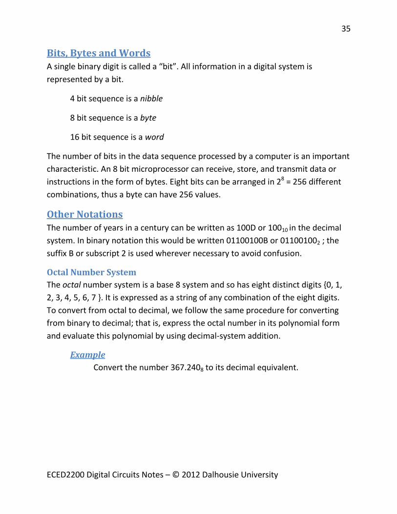
Octal Number System The octal number system is a base 8 system and so has eight distinct digits {0, 1, 2, 3, 4, 5, 6, 7 }. It is expressed as a string of any combination of the eight digits. To convert from octal to decimal, we follow the same procedure for converting from binary to decimal; that is, express the octal number in its polynomial form and evaluate this polynomial by using decimal-system addition.
Example Convert the number 367.2408 to its decimal equivalent.

36
ECED2200 Digital Circuits Notes – © 2012 Dalhousie University
To convert from decimal to octal we use the same procedure as converting from decimal to binary, but instead of diving by 2 for the integer part, divide by 8 to obtain the octal equivalent. Also, instead of multiplying by 2 for the fractional part, multiply by 8 to obtain the fractional octal equivalent of the decimal system. However, it is more common to convert from binary to octal and vice-versa.
The conversion from binary to octal is accomplished by grouping the binary numbers into groups of 3 bits each, starting from the binary point and proceeding to the right and to the left. Each group is then replaced by its octal equivalent.
Example Convert 011001002 into its octal equivalent.
Grouping the bits into groups of 3 bits from the binary point we get:
001 100 100
Note that a leading zero was added to complete the first group. Each group is now replaced by its octal equivalent to get:
001 100 100
1 4 4
Thus,
011001002 = 144 O = 1448
The three-bit octal numbers are easier to work with than their 8-bit binary equivalents.
37
ECED2200 Digital Circuits Notes – © 2012 Dalhousie University
To convert from octal to binary replace each octal digital by its 3-bit binary equivalent.
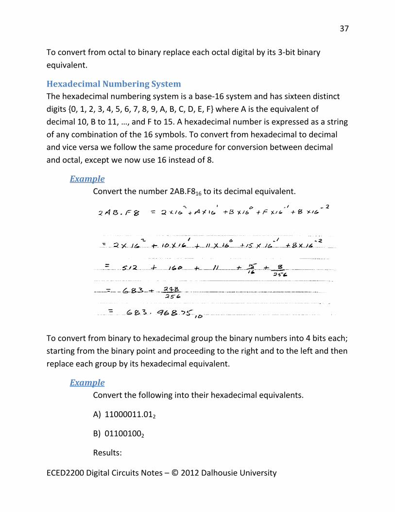
Hexadecimal Numbering System The hexadecimal numbering system is a base-16 system and has sixteen distinct digits {0, 1, 2, 3, 4, 5, 6, 7, 8, 9, A, B, C, D, E, F} where A is the equivalent of decimal 10, B to 11, …, and F to 15. A hexadecimal number is expressed as a string of any combination of the 16 symbols. To convert from hexadecimal to decimal and vice versa we follow the same procedure for conversion between decimal and octal, except we now use 16 instead of 8.
Example Convert the number 2AB.F816 to its decimal equivalent.
To convert from binary to hexadecimal group the binary numbers into 4 bits each; starting from the binary point and proceeding to the right and to the left and then replace each group by its hexadecimal equivalent.
Example Convert the following into their hexadecimal equivalents.
A) 11000011.012
B) 011001002
Results:

38
ECED2200 Digital Circuits Notes – © 2012 Dalhousie University
A) Group the bits into groups of 4 bits from the binary point and replace each group by its hexadecimal equivalent:
Thus 11000011.012 = C3.416.
B)
Thus 011001002 = 64H = 6416.
To convert from hexadecimal to binary replace each hexadecimal digit by its 4-bit binary equivalent. A table of the four number systems is given below:

39
ECED2200 Digital Circuits Notes – © 2012 Dalhousie University
Signed Magnitudes In binary notation, an n-bit data word can represent the first 2n non-negative integers. To allow for both positive and negative numbers, the most significant bit (MSB) can be designated as the sign bit (0 for positive numbers, 1 for negative numbers). The lower order bits then represent the magnitude of the number in binary notation.
The figure below shoes a “number where” representation of a 4-bit number system. The figure shows the binary numbers and their decimal integer equivalents, assuming that the numbers are interpreted as sign and magnitude.

40
ECED2200 Digital Circuits Notes – © 2012 Dalhousie University
The largest positive number that can be represented in three data bits is +7 = 23 – 1. Similar the smallest negative number is -7.
This method has the following disadvantages:
• The number zero has two different representations • Two different arithmetic circuits are required to process positive and
negative numbers, see the following straight-binary example giving incorrect answers:
Complements A better notation for computers is based on the fact that adding the complement of a number is equivalent to subtracting the number. Hence instead of performing A-B using a subtractor, we can perform A + (-B) to obtain the same result using an adder.
For each base r system, there are two types of complements, namely, the radix complement, also known as the r’s complement, and the diminished radix complement, also known as the (r-1)’s complement.

41
ECED2200 Digital Circuits Notes – © 2012 Dalhousie University
Radix Complement The radix complement, denoted by [N]r , for a n-digital and r-base number (N)r is defined as follows:
Example:
A) Obtain the 2-digit 10’s complement of 15 and 24.
B) Represent -15 and -24 in 8-bit signed 2’s complement notation.
Answers:
A) 1510 = 102 – 15 = 100 – 15 = 85
2410 = 102 – 24 = 100 – 24 = 76
B) In binary:

42
ECED2200 Digital Circuits Notes – © 2012 Dalhousie University
and:
The 2’s complement of a binary number can be obtained directly from the given number of copying each bit of the number, starting at the lest significant bit, and proceeding towards the most significant bit until the first 1 has been copied. After the first 1 has been complied, replaced each of the remaining 0’s and 1’s by 1’s and 0’s respectively.

43
ECED2200 Digital Circuits Notes – © 2012 Dalhousie University
Example
The 4-bit 2’s complement number representation is shown below. Note there is only one representation for zero.
A) Represent -15 and -24 in 8-bit signed 2’s complement notation.
Convert 1111 to 8-bit number:
00001111
Starting from left-hand side, invert each bit until the last ‘1’ is encountered:
11110001
Therefore -15 is 11110001 in signed 2’s complement.

44
ECED2200 Digital Circuits Notes – © 2012 Dalhousie University
Again convert to 8-bit number:
00011000
Starting from left-hand side, invert each bit until the last ‘1’ is encountered:
11101000
Therefore -24 is 11101000 in signed 2’s complement.
The 4-bit 2’s complement number representation is shown below. Note there is only one representation for zero.
Two’s Complement Arithmetic
Addition Two n-bit signed binary numbers in 2’s complement format are added by performing a binary addition of the two numbers, including the sign bits. If a carryover bit results from the leftmost bit, it is discarded. The leftmost bit of the result will give the sign of the sum.
If the sign bit is a 1 we must take the 2’s complement of the result to get the real magnitude of the final answer.

45
ECED2200 Digital Circuits Notes – © 2012 Dalhousie University
Subtraction In 2’s complement format subtraction of two signed numbers is performed by adding the 2’s complement of the subtractand to the numerand. If a carryover results from the leftmost bit, it is discarded. Also the leftmost bit gives the sign of the difference.
Note that the 10’s complement can be obtained by forming the 9’s complement and adding 1. The 2’s complement can be obtained by forming the 1’s complement ad adding 1. The 1’s complement is formed by changing 1’s to 0’s and 0’s to 1’s. The 1’s complements representation is shown below. Note the two representations of zero:
Example Perform (A) 24-15 and (B) 15-24 directly and by complement notation.
Answers:
A) Direct
10’s Complement

46
ECED2200 Digital Circuits Notes – © 2012 Dalhousie University
2’s Complement
B) Direct
10’s Complement
2’s complement

47
ECED2200 Digital Circuits Notes – © 2012 Dalhousie University
Note that for the 10’s complement the carryover is discarded and if the result is negative the complement must be taken to get the final result.
Binary Coded Decimal For convenience, computer input/output devices may accept/provide decimals on the human side and binaries on the computer side. In a binary-coded decimal number each of the decimal digital is coded in binary, using 4 bits. For example in the 8421 code 610 = 01102, 310 = 0112, and 363 = 0011 0110 0011 BCD.
When a computer is to handle letters as well as numbers, the alphanumeric code is used. In the American Standard Code for Information Interchange (ASCII) seven bits are used to represent all the characters and punctuation marks on a teletypewriter keyboard plus some control signals. Note that 27 = 128 combinations of 7 bits. An eighth bit, the MSB, is a parity bit used in error correction. In the even parity connection, the MSB is set so that the number of 1’s in each ASCII character is even, the present of an odd number of 1’s indicates an error.

48
ECED2200 Digital Circuits Notes – © 2012 Dalhousie University
Boolean Algebra Boolean algebra is useful in manipulating binary variables (0,1) in OR, AND, or NOT relations and in the analysis and design of all types of digital systems.
Boolean Theorems The basic postulates are given in the tables below. In general, the inputs and outputs are variables (either 1 or 0).
Boolean Postulates in 0 and 1

49
ECED2200 Digital Circuits Notes – © 2012 Dalhousie University
Basic Boolean Identities No. Identity Comments 1 A+0=A Operations with 0
and 1 2 A+1=1 Operations with 0
and 1 3 A+A=A Idempotent 4 A+A=1 Complements 5 A 0=0• Operations with 0
and 1 6 A 1=A• Operations with 0
and 1 7 A A=A• Idempotent 8 A A=A• Complements 9 A=A 10 A+B=B+A Commutative 11 A B=B A• • Commutative 12 A (B+C)=(A+B)+C=A+B+C+ Associative 13 A (B C)=(A B) C=A B C• • • • • • Associative 14 A (B+C)=(A B)+(A C)• • • Distributive 15 A+(B C)=(A+B) (A+C)• • Distributive 16 A+(A B)=A• Absorption 17 A (A B)=A• + Absorption 18 (A B)+(A C)+(B C)=(A B)+(A C)• • • • • Consensus 19 A+B+C+...=A B C...• • De Morgan 20 A B C ...=A B C...• • • + + De Morgan 21 (A+B) B=A B• • Simplification 22 (A B) B=A B• + + Simplification
The validity of the 22 rules can be verified by substituting all possible values for the Boolean variables and evaluating the left and right-hand sides of each identity. This is known as a proof by perfect induction.

50
ECED2200 Digital Circuits Notes – © 2012 Dalhousie University
Example: Use proof by induction to verify the consensus identity:
Note that when B●C=1, this means B=C=1. One of the remaining terms will always be 1 in that case, which is why B●C is redundant.
The first nine identities are the fundamental relations of Boolean algebra. Identities 10-14 are similar to the laws of ordinary algebra. Identities 10 and 11 are the commutative rules, 12 and 13 are the associative rules, and 14 and 16 are the distributive rules. Identities 16-18 do not apply to ordinary algebra but are very useful in Boolean Algebra. Identities 16 and 17 are the absorption identities; identity 18 is the consensus identity; identity 19 and 20 are De Morgan’s rules. Formally identities 21 and 22 are simplification rules.
The basic identities can be used to simplify Boolean functions.
Example Derive the absorption rule:

51
ECED2200 Digital Circuits Notes – © 2012 Dalhousie University
Using other basic theorems.
De Morgan’s Theorems De Morgan’s theorems are easily interpreted in terms of logic circuits. The first says that a NOR gate is equivalent to an AND gate with NOT circuits in the inputs. The second says that a NAND gate is equivalent to an OR gate with NOT circuits in the inputs. As started by Shannon, De Morgan’s theorem says:
To obtain the inverse of any Boolean function, invert all variables and replace all OR’s by AND’s and all AND’s by OR’s.
Example Use De Morgan’s theorems to design a combination of NAND gates equivalent to a two-input OR gate.
The desired function is:

52
ECED2200 Digital Circuits Notes – © 2012 Dalhousie University
Using De Morgan’s theorem (Identity 19) we get:
Suggesting a NAND gate with NOT inputs because by theorem 7, a NAND gate with the inputs tied together performs the NOT operation. The logic circuit is shown below:
Logic Circuit Analysis The Boolean identities permit us to manipulate logic statements or functions directly, without setting up truth tables. Also, the use of Boolean algebra can lead to simpler logic statements that are easier to implement. De Morgans theorems are useful in finding NAND operations that are equivalent to other operations.
The analysis of a logic circuit consists in writing a logic statement expression the overall operation of the circuit. This can be done by starting at the input and tracking through the circuit noting the function realized at each output. The resulting expressions can be simplified or put into an alternate form by using Boolean Algebra. A truth table can be constructed.
Note the symbol A●B can be simplified to AB or A(B).
Example Analyze the given logic circuit:

53
ECED2200 Digital Circuits Notes – © 2012 Dalhousie University
Construct the truth table to demonstrate that this circuit could be replaced by a single NAND gate.
The suboutputs are as noted on the diagram. The overall function can be simplified as follows:
The truth table is given below:

54
ECED2200 Digital Circuits Notes – © 2012 Dalhousie University
Two-Level Combinational Logic A two-level implementation means that there are only two gates between input and output. A two-level implementation of f A B C D= • + • is shown below:
Each appearance of a variable or its complement is an expression is called a literal. Combinational networks are those where the outputs depend only on the current input. They are circuits without a memory.

55
ECED2200 Digital Circuits Notes – © 2012 Dalhousie University
Logic Circuit Synthesis The logic designer starts with a logic statement or truth table, converts the logic function into a convenient form and then realizes the desired functions by means of a standard or special logic Elements.
Adding
The Half Adder Consider the process of addition. In adding two binary digits, the possible sums are shown below. Note that when A=1 and B=1, the sum in the first column is 0 and there is a carry of 1 to the next higher column.
As indicated in the truth table, the half-adder must perform as follows: “s is 1 if A is 0 AND B is 1, OR if A is 1 AND B is 0; c is 1 if A AND B are 1”. In logic nomenclature, this becomes:
Which can be written as:

56
ECED2200 Digital Circuits Notes – © 2012 Dalhousie University
Note that a full-adder can accept the carry from the adjacent column.
To synthesize a half-adder circuit, start with the output and work backwards. The above equation indicates that the sum s is the output of an OR gate; the inputs are obtained from AND gates; inversion of A and B is necessary. The above expression also indicates that the carry c is the output of an AND gate. The logic circuit is shown below.
Different Boolean expressional are possible for a given logic statement and some will lead to better circuit realizations than others. Consider the last expression:

57
ECED2200 Digital Circuits Notes – © 2012 Dalhousie University
And referring to the truth table we see that another interpretation is:
“S is 1 if (A OR B) is 1 AND (A AND B) is NOT 1”. The binary addition is:
The synthesis of the circuit, working backwards from the output, is shown below:
The circuit is better than the previous one in that fewer logic elements are used and the longest path from input to output passes through fewer levels.

58
ECED2200 Digital Circuits Notes – © 2012 Dalhousie University
In terms of the Exclusive-OR gate, the half-adder takes the simple form shown below:
The half adder can be treated as a discreet logic element and represented as shown below:
The Full Adder To add two binary digits (bits) the half-adder performs the most elementary part. For a complete addition we need a fill-adder capable of handling the carry input as well. The addition process is illustrated below where ci is the carry from the proceeding column:

59
ECED2200 Digital Circuits Notes – © 2012 Dalhousie University
Each carry of 1 must be added to the two digits in the next column, so the logic circuit must be able to combine three inputs. The truth table for the full-adder is shown below.
Note that both S and Co have four cases with 1’s in the output columns. In logic notation we have:

60
ECED2200 Digital Circuits Notes – © 2012 Dalhousie University
The expression for Co can be simplified as follows:

61
ECED2200 Digital Circuits Notes – © 2012 Dalhousie University
Although this leads to a simpler expression, applying the rules of Boolean algebra in this situation does not guarantee the simplest expression. A more systematic approach will be discussed later.
Using the expression for S and Co the full adder can be implemented as shown below:
The full adder can also be implanted with two half-adders and one OR gate, as shown below:
For this case the S output from the second half-adder is the Exclusive-OR of Ci and the output of the first half-adder, giving:

62
ECED2200 Digital Circuits Notes – © 2012 Dalhousie University
as before. The carry out is the (Exclusive-OR of A and B AND Ci) OR’ed with A AND B, or:
as before.
The full adder can be treated as a discreet logic element and represent as shown below:

63
ECED2200 Digital Circuits Notes – © 2012 Dalhousie University
To obtain the binary addition of two n-bit binary numbers, we cascade n full-adder circuits together, with the carry in of a full-adder being connected to the carry out of the previous full adder. The interconnection of four full-adders to provide the addition of two 4-bit binary numbers is shown below:
Note that the initial adder need only be a half-adder since the initial Ci is 0.
MSI (Medium Scale Integration) packages are available that contain 4 and 8-bit binary adders.
Subtraction
Direct Approach Subtraction can be implemented with logic circuits in a direct manner as was done for adders. In this method the subtractend is subtracted from the numerend to form the difference. If the numerend is smaller than the subtractend, a 1 is borrowed from the next significant position. This borrow must be conveyed to the next stage. As in the case of adders, there are half- and full-subtractors.

64
ECED2200 Digital Circuits Notes – © 2012 Dalhousie University
Indirect Approach (Using Adders) As discussed earlier, subtraction may be accomplished by taking the complement of the subtractend and adding it to the numerend. Subtraction then becomes addition requiring full-adders for machine implementation. The addition and subtraction operation can be combined into one circuit with the common binary adder. This is done by including an Exclusive-OR gate with each full adder as shown below. The mode input (M) controls the operation. When M=0, the circuits is an adder, and when M=1, the circuit becomes a subtractor. Each Exclusive-OR gate has input M and one of the inputs of B (Bi).
When M=0, we have Bi XOR 0 = Bi. The full-adders receive the value Bi, the input carry is 0, and the circuit performs A+B. When M-1, we have Bi XOR 1 = NOT Bi, and the input carry is 1. The Bi inputs are all complemented and a 1 is added through the input carry. The circuit performs (A + NOT(B) + 1) which is A plus the 2’s complements of B. Note that NOT(B) is actually the 1’s complement, but also called the “diminished 2’s complement”.
Arithmetic Logic Unit (ALU) A arithmetic logic unit (ALU) is a combinational network of logic gates arranged to perform addition, complementing, incrementing, and the associated register for temporary storage of data or results. The ALU is governed by a control unit, which sets the various logic gates, feeds the numeric data, and provides the clock pulse

65
ECED2200 Digital Circuits Notes – © 2012 Dalhousie University
that regulates the speed of operation. An ALU and its control unit for an elementary example are shown below.
In this case the stored number A and B are operated according to the instruction in the form of a 4-bit word. The instruction is taken from memory and placed in a register. The instruction 1011 shown sets the logic gates so that A, B, and 0 are available for processing. Other instructions and the outputs are shown in the table below. There are 24 = 2 x 32 possibilities.
A Design Procedure In logic design, gates must be combined to realize the desired function. The design proceeds according to the following steps.

66
ECED2200 Digital Circuits Notes – © 2012 Dalhousie University
1. Statement of function 2. Form a truth table 3. Obtain the Boolean expression of the function 4. Manipulate the Boolean expression to the simplest form 5. Realize in terms of AND, OR and NOT gates
Example For increased reliability on a spacecraft triple sensing systems are used; no action is taken unless at least two of those systems call for action. The required system is known as a vote taker whose truth table is shown below:
Because the function is YES(1) only when a majority of inputs are YES, the Boolean expression is:

67
ECED2200 Digital Circuits Notes – © 2012 Dalhousie University
If the complement of each variable is available (true in most computers), the realization is a combination of four AND gates feeding an OR gate:
If the complements are not available eight logic elements (three NOT elements) would be required, and simplification of the circuit is desirable. We proceed as follows:

68
ECED2200 Digital Circuits Notes – © 2012 Dalhousie University
This function requires only four logic elements as shown below:

69
ECED2200 Digital Circuits Notes – © 2012 Dalhousie University
Two-Level Canonical Forms A Boolean function can be written in different forms. Certain forms, however, lead to more desirable combinational networks. These forms which are canonical forms are of two types: sum of products and product of sums.
Sum of Products We have used the sum of products form in our earlier work. A sum of products expression is formed as follows. Each row of the truth table in which the function takes on the value 1 contributes an ANDed term. These are called minterms. A minterm is defined as an ANDed product of literals in which each variable appears exactly once in either normal or complemented form, but not both. The minterms are then ORed to form the expression for the function. The minterm expression is equivalent since it is derived from the truth table.
The figure below shows a truth table for an arbitrary function f and its complement. The minterms and maxterms for each row are also shown. The minterm expressions for f and f NOT are:
Truth table which above is based on:

70
ECED2200 Digital Circuits Notes – © 2012 Dalhousie University
The above expression can be written in a shorthand notation. Note that the indexing of the Boolean variables is important in deriving the minterm and maxterm. In shorthand notation we have:
Where means the sum of all the minterms whose subscript i is given inside the parentheses.
The minterm expression is not likely to be the simplest form of the function. The expression for f can be reduced by using Boolean algebra.

71
ECED2200 Digital Circuits Notes – © 2012 Dalhousie University
The minimized gate-level implementation of f is shown below:
The expression f NOT can also be reduced:

72
ECED2200 Digital Circuits Notes – © 2012 Dalhousie University
Product of Sums A product of sums expressions is formed as follows. Each row of the truth table in which the function takes on the value 0 contributes an ORed therm. These are called maxterms. A maxterm is defined as an ORed sum of literals in which each variable appears exactly once in either true or completed form, but not both. The maxterms are then ANDed to form the expression for the function. This is opposite to the way we formed minterms.
The products of sum of functions f and f NOT is obtained from the truth table as:
Using a shorthand notation we can write f and f NOT as:
Where means the product of all the maxterms whose subscript I is given inside the parentheses.
Conversion Between Canonical Forms One canonical form can be mapped into the other by applying De Morgan’s Theorem. For example if we apply DeMorgan’s Theorem to the minterm expansion of f NOT we get:

73
ECED2200 Digital Circuits Notes – © 2012 Dalhousie University
Or:
Which is the maxterm expansion of f. Similarly applying DeMorgan’s Theorem to them maxterm expansion of f NOT gives:
Or using 19:
Which is the maxterm expansion of f.
The minimized product of sums form can be found by starting with the minimized sum of products form of f NOT and using DeMorgan’s Theorem.

74
ECED2200 Digital Circuits Notes – © 2012 Dalhousie University
Or using 20:
The minimized gate-level implementation is shown below:
Positive Versus Negative Logic So far, we have assumed that logic 1 is represented by a higher voltage than logic 0. This is known as positive logic. If we use the low voltage to represent the asserted signal and the high voltage to represent the unasserted signal we have negative logic.
Consider a truth table given in terms of high and low voltages:

75
ECED2200 Digital Circuits Notes – © 2012 Dalhousie University
In the positive logic case the truth table describes an AND function, whereas, in the negative logic case we obtain an OR function. This is to be expected since an AND function and an OR function are duals, by replacing 0’s in one truth table with 1’s in the other, and vice versa.
Given a function is positive logic, the equivalent negative logic can be found by applying duality. For example the dual of the NOR function is the NAND function.

76
ECED2200 Digital Circuits Notes – © 2012 Dalhousie University
Minimization by Mapping The optimum form of a logic circuit is desired. The criteria is often ONE of the following:
a) Maximum speed – fastest logic implementation
Or:
b) Minimum cost – fewest gate levels because the number of levels determines the cost of manufacturing and the cost of assembly.
Or:
c) Minimum design time – if only a few circuits are required
Boolean algebra can be used to devise simpler logic expressions. If the truth table is available or if the logic function is expressed as a sum of products we can go directly to a minimum expression by a mapping technique from Maurice Karnaugh.
Karnaugh Maps (K-Maps) The K-map of the general logic function of three variables is shown below. Each square in the map corresponds to one of the eight possible combinations of the three variables. The order of the columns is such that combinations in adjacent squares different only in the value of one variable.

77
ECED2200 Digital Circuits Notes – © 2012 Dalhousie University
We see that 2-square groups are independent of one variable. E.g.: for the groups circled:
As shown above those relations are easily determined using Boolean algebra, but they are obvious by inspection of the K-maps.
We can extend the groupings from adjacent squares as shown below where the labels are omitted from the squares.
We see that 4-square groups are independent of the variables, e.g.:

78
ECED2200 Digital Circuits Notes – © 2012 Dalhousie University
Enlarging groups by overlapping simplifies the table. Note that the map is continuous, in that the last column on the right is “adjacent” to the first column in the left:

79
ECED2200 Digital Circuits Notes – © 2012 Dalhousie University
The standard labeling for K-maps (shown below) is convenient for mapping from the truth table.

80
ECED2200 Digital Circuits Notes – © 2012 Dalhousie University
Each square in the map corresponds to a row in the truth table. A specific logic function is mapping by placing a 1 in each square for which the function is 1. Possible simplifications are then easily recognized.
Example Map the vote-taker function and simplify the circuit realization, if possible. From the truth table of the vote taker function:
We first place 1’s in the squares corresponding to the tows in the truth table for which the result of the function is 1, resulting:

81
ECED2200 Digital Circuits Notes – © 2012 Dalhousie University
All the 1’s can be included in three overlapping 2-square groups. The complete function can be represented by:
This is the simplest expression for the function. By using DeMorgan’s Theorem, any “sum of products” can be converted into a “NANDed product of NAND’s”. In this case:
Which can be synthesized using NAND gates only:
Example Map the full-adder sum and conjugate functions. Obtain the simplest forms of the function. The truth table is as follows:

82
ECED2200 Digital Circuits Notes – © 2012 Dalhousie University
Because there is two output functions, we have two separate K-maps:

83
ECED2200 Digital Circuits Notes – © 2012 Dalhousie University
From the K-maps we see that the simplest form for the sum is given by:
And the simplest form for the conjugate is given by:
Both of these results agree with the earlier results. Note that the conjugate function is the same as the vote-taker function of the last example.
Mapping in Four Variables K-maps are useful in simplification functions involving four variables. Typically once more than four variables are involved it becomes easier to use other techniques. A four-variable K-map is shown below:

84
ECED2200 Digital Circuits Notes – © 2012 Dalhousie University
As indicated in the figures below (where standard labeling for K-maps is used):
• 2-square groups are independent of one variable • 4-square groups are independent of two variables • 8-square groups are independent of three variables
Note that adjacent rows different by only one complement bar, and the bottom row is adjacent to the top row with the left column adjacent to the right.

85
ECED2200 Digital Circuits Notes – © 2012 Dalhousie University
The four corner squares for the groups .
Some general guidelines for finding the minimal expression for a K-map are:
a) Include all 1’s in groups of eight, four, two, or one. b) Groups may overlap; larger groups result in simpler terms c) Of the possible selection of terms, select the simplest
Example Map the function:
And obtain a minimum sum of products expression.
Using DeMorgan’s theorem the given expression can be written as:
The K-map is given below:

86
ECED2200 Digital Circuits Notes – © 2012 Dalhousie University
All the 1’s can be included in two 4-square and one 2-square groups. Thus:
Note that the other expressions are possible but none with fewer, simpler terms.
Example Map the function:
And find the minimal sum of products form
The K-Map is shown below:
From the map we see that the minimum f is:

87
ECED2200 Digital Circuits Notes – © 2012 Dalhousie University
Again other arrangements are possible, but not minimal.
Five-Variable Maps Maps for more than four variables are not as simple to use. A five-variable map needs 32 squares and a six-variable map needs 64 squares. With a large number of variables the number of squares is large and the geometry for combining adjacent squares is made convoluted.
The five-variable map shown below consist of 2 four-variable maps with variables, A,B,C,D, and E. Variable A distinguishes between the two maps. The left-hand four-variable map represents the 16 squares where A=0, and the other four-variable map represents the squares where A=1. Minterms 0 through 15 belong with A=0, and minterms 16 through 31 with A=1. Note that the numbering of the minterms is important.
Each four-variable map retains the previously defined adjacency when taken separately. In addition, each square in the A-0 map is adjacent to the corresponding square in the A=1 maps. For example, minterm 4 is adjacent to minterm 20 and minterm 15 to 31. The best way to visualize this new adjacency rile is to cascade the two half maps as being one on top of the other. Any two squares that fall one over the other are considered adjacent:

88
ECED2200 Digital Circuits Notes – © 2012 Dalhousie University
Example Simplify the Boolean function:
The filled in K-map is shown below, along with the simplified function:

89
ECED2200 Digital Circuits Notes – © 2012 Dalhousie University
Note the redundant agency has been omitted.
By following the procedure used for the five variable maps, it is possible to construct a six-variable map using four of the 4-variable maps to obtain the required 64 squares. For maps with N variables one must check for adjacencies in N directions. Maps with six or more variables need too many squares and are impractical to use. It is simpler to use computer programs written to simplify Boolean functions with a large number of variables.
Comments on Maps 1. Two variable K-maps are shown below:

90
ECED2200 Digital Circuits Notes – © 2012 Dalhousie University
2. An N-Variable K-map has 2N cells.
3. In some circuits, certain combinations of inputs never occur. These don’t
care combinations map be mapped as X’s and considered as either 0’s or 1’s, whichever provides the greatest simplification.
4. In some circuits the simplest realization results from finding f NOT as the sum of products and then inverting the result to obtain f.
5. The K-map can be used to find the minimum product of sums expression. In this case we collect the maximal adjacent group of 0’s and write the functions complement in the sum of product forms. Applying DeMorgan’s Theorem we get the product of sums form.
Example of Points 4&5: Given the following K-Map:

91
ECED2200 Digital Circuits Notes – © 2012 Dalhousie University
Find f in the minimum product of sums form.
From the map we see that:
Therefor:
Using DeMorgan’s Theorem we get:

92
ECED2200 Digital Circuits Notes – © 2012 Dalhousie University
Example Use K-maps to synthesize a 2-bit binary adder whose diagram and truth table are given below:
The adder has two 2-bit binary numbers N1 and N2 as inputs and produces a 3-bit number, N3, as an output. In the truth table N1 is represented by the inputs A&B, and N2 by C&D. The output is represented by the Boolean function X,Y, and Z.
The K-maps for the outputs are shown below. From the maps we can write the function X, Y, and Z:

93
ECED2200 Digital Circuits Notes – © 2012 Dalhousie University

94
ECED2200 Digital Circuits Notes – © 2012 Dalhousie University
The functions can be synthesized as shown below:
Some More Notes: Implicants 1) An implicant of a function f is a single or group of elements that can be
combined together in a K-map.

95
ECED2200 Digital Circuits Notes – © 2012 Dalhousie University
2) A prime implicant is an implicant that cannot be combined with another
one to eliminate a literal.
3) If a particular element is covered by a single prime implicant, it is called an essential prime implicant.
Example The logic box for a controller with inputs S2, S1, S0, C1, and C2 has to be designed using combinational logic gates. For the truth tables given below where B, I and R are outputs. Use the five variable K map procedure to draw the minimum circuit necessary to complete the table.

96
ECED2200 Digital Circuits Notes – © 2012 Dalhousie University
The resulting K-Maps are shown below:

97
ECED2200 Digital Circuits Notes – © 2012 Dalhousie University

98
ECED2200 Digital Circuits Notes – © 2012 Dalhousie University
From the K-maps we see that:
The minimum circuit is shown below:

99
ECED2200 Digital Circuits Notes – © 2012 Dalhousie University

100
ECED2200 Digital Circuits Notes – © 2012 Dalhousie University
Multilevel Combinational Logic Consider the function:
Which is in its numerical sum of products form. The corresponding logic circuit is shown below:
We see that as a two-level network of AND and OR gates it requires six 3-input AND gates and one 7-input OR gate for a total of seven gates and 19 literals.
We can replace the two-level form with a factored form as follows:

101
ECED2200 Digital Circuits Notes – © 2012 Dalhousie University
Or:
The corresponding circuit is shown below:
The result is a three (3) level network which requires one 3-input OR gate, two 2-input OR gates, and a 3-input AND gate for a total of four gates and seven literals.
We have reduced the number of wires and gates required but this implementation probably has more delay because of the increased levels of logic. In general, multilevel circuits are more gate efficient than the corresponding two-level circuits but have worse propagation delay.

102
ECED2200 Digital Circuits Notes – © 2012 Dalhousie University
Conversion to NAND and NOR Networks The canonical forms studied so far are expressed in terms of AND and OR gates. In practice it is more efficient to use NAND and NOR gates. We will now see how to map a network with AND and OR gates into that consisting only of NAND or NOR gates.
As can be seen from the truth tables below:
i) An OR gate is logically equivalent to a NAND gate with its inputs inverted ii) A NAND gate is equivalent to an OR gate with its inputs inverted iii) An AND gate is equivalent to a NOR gate with its inputs inverted iv) A NOR gate is equivalent to an AND gate with its inputs inverted
The graphic symbols for each gate are shown below:
To obtain a multilevel NAND circuit from a Boolean expression, proceed as follows:

103
ECED2200 Digital Circuits Notes – © 2012 Dalhousie University
1. From the given Boolean expression, draw the logic diagram with AND, OR, and NOT inverter gates. Assume that both the normal and complement inputs are available.
2. Convert all AND gates to NAND gates with AND-invert graphic symbols:
3. Convert all OR gates to NAND gates with invert-OR graphic symbols:
4. Check all small circles in the diagram. For every small circle that is not
compensated by another small circle along the same long, insert an inerter (one-input NAND gate) or complement the input variable:
Example Given the function:

104
ECED2200 Digital Circuits Notes – © 2012 Dalhousie University
Draw the logic diagram in the AND/OR form and convert to NAND logic.
The AND/OR form is shown below:
There are four levels of gates in the circuit. Using the procedure given earlier obtain the NAND diagram using two symbols:

105
ECED2200 Digital Circuits Notes – © 2012 Dalhousie University
Note that the literal B input to the second level NAND gate must be inverted to preserve the original sense of the signal. Since it does not matter whether we use AND-invert or the invert-OR symbols to represent a NAND gate, the diagram below is identical to the one above:
To obtain a multilevel NOR circuit from a Boolean expression, proceed as follows: 1. Draw the AND-OR logic diagram from the given algebraic expression.
Assume that both the normal and complement inputs are available.
2. Convert all OR gates to NOR gates with OR-invert graphic symbols:
3. Convert all AND gates to NOR gates with invert-AND logic symbols:
4. Any small circle that is not complemented by another small circle along
the same line needs and inverter or the complementation of the input variables.

106
ECED2200 Digital Circuits Notes – © 2012 Dalhousie University
Example Convert the function f of the last example to NOR logic.
Using the above procedure the AND/OR form is convert to the NOR diagram below:

107
ECED2200 Digital Circuits Notes – © 2012 Dalhousie University
Note the extra inversion required at the output. The final NOR only circuit is shown below:
The inversion at the output has been implemented by a NOR gate with both inputs tied to the same signal.

108
ECED2200 Digital Circuits Notes – © 2012 Dalhousie University
Computer Aided Design Tools Computer-Aided Design (CAD) is used to speed up the high level design process. Besides allowing the exploration of design alternatives, design tools can improve the quality of the design by simulating an implementation before physical construction. Packages such as MIS-II developed at the University of California at Berkley are available for this purpose.
NOTE: Since these notes were written a huge variety of newer tools are available. One of the more popular is Eagle (www.cadsoftusa.com) although it has more limited simulation support. Autotrax (www.kov.com) has fairly good simulation support and an easier user interface.

109
ECED2200 Digital Circuits Notes – © 2012 Dalhousie University
Time Response in Combination Networks The propagation of signals through a network is not instantaneous. These delays may lead to logical errors at the outputs. Delays come from several sources:
Gate Delays
A gate delay is the amount of time it takes for a change at the gate input to cause a change at the output. Various families of TTL have trade-offs between delay and power. The faster a component, the more power it consumes. Propagation delays often depend on whether the output is going from a low to high (tLH) or from high to low (tHL). For example for the 7400 gate a typical tHL
= 7nS and tLH = 11 nS.
Timing Waveforms As an example of a timing waveform consider the circuit shown below:
An input signal A passes through three inverters and is then ANDed with the original signal. This implements the function:
This appears to be a useless function. However, examining the timing diagram below shows that after the input A goes high, the output goes high for a short time before going low. This circuit is called a pulse shaper.

110
ECED2200 Digital Circuits Notes – © 2012 Dalhousie University
To see how the circuit operations, assume that the initial state has A=0, B=1, C=0, D=1, and f=0 as shown at t=0. Further, assume that each gate has a propagation delay of 10 time units. When A changes from 0 to 1 at time 10, B does not change until time step 20, C at time step 30, and D at time step 40. We see that between time 10 and 40, both A and D are at logic 1. If the AND gate also has a 10-unit gate delay, the output f will be high between time stops 20 and 50. The pulse f is three inverter delays wide. To change the width, use a different number of inverters.

111
ECED2200 Digital Circuits Notes – © 2012 Dalhousie University
Hazards and Glitches A glitch is an unintended pulse at the output of a combinational logic network. A circuit with the potential for a glitch is said to have a hazard.
The circuit below demonstrates the occurrence of a hazard. Assume that all inputs are initially 1. The output of gate 1 will then be 1, that of gate 2 will be 0, and the output of the circuit will be 1.
Let B change from 1 to 0. The output of gate 1 changes to 0 and that of gate 2 changes to 1, leaving the output at 1. The output may momentarily go to 0 if the delay through the inverter is large enough. The delay may cause the output of gate 1 to change to 0 before the output of gate 2 changes to 1. In this case both inputs to gate 3 are momentarily equal to 0, causing the output to go to 0 for a short time.
The figure below is a NAND implementation of the same Boolean function. It has a hazard for the same reason:
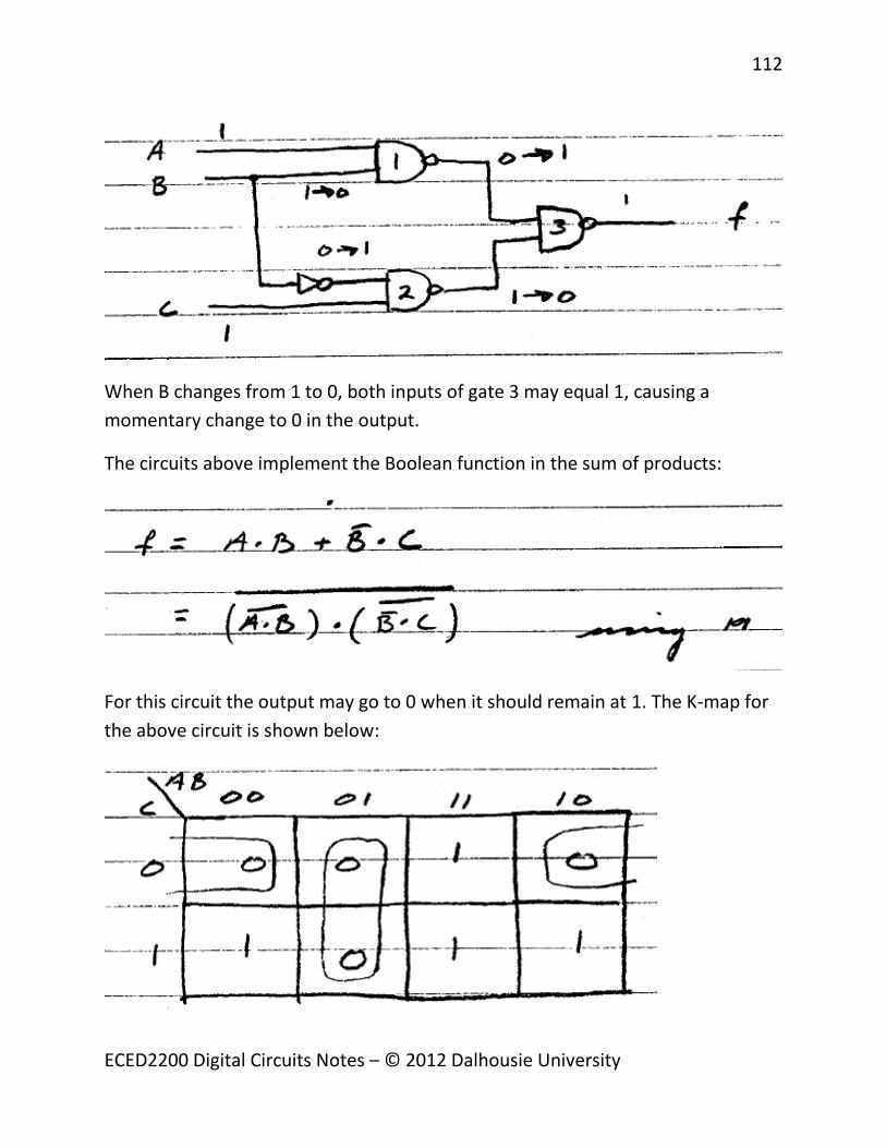
112
ECED2200 Digital Circuits Notes – © 2012 Dalhousie University
When B changes from 1 to 0, both inputs of gate 3 may equal 1, causing a momentary change to 0 in the output.
The circuits above implement the Boolean function in the sum of products:
For this circuit the output may go to 0 when it should remain at 1. The K-map for the above circuit is shown below:

113
ECED2200 Digital Circuits Notes – © 2012 Dalhousie University
From the zero location the circuit can be implemented in product of sum form:
In this form the output may momentarily go to 1 when it should remain 0. The first case is a static 1-hazard and the second case is a static 0-hazard. A third type of hazard known as a dynamic hazard causes the output to change three or more times when it should change from a 1 to 0 or from a 0 to 1. The figure below shows the three types of hazards:
The occurrence of a hazard can be detected by inspecting the K-maps of the particular circuit. For example consider the K-map of the above AND-OR circuit:
The change in B from 1 to 0 moves the circuit from minterm 111 to minterm 101. The hazard exists because the change of input results in a different product term implicant covering the two minterms. Minterm 111 is covered by the product term implemented in gate 1, and minterm 101 is covered by the product term implemented in gate 2. Whenever the circuit moves from one product term to

114
ECED2200 Digital Circuits Notes – © 2012 Dalhousie University
another, there is a possibility of a momentary interval when neither term is equal to 1, giving rise to an undesirable 0 output.
Hazards can be eliminated by enclosing the two minterms in a function with another product term that covers both groupings. This is shown in the K-map below:
The hazard-free circuit is shown below. The extra gate in the circuit generates the product term A●C. The removal of the hazard requires the addition of redundant gates to the circuit.
Notes 1. In two-level networks when a circuit is synthesized in sum of
products with AND-OR gates or with NAND gates, the removal of static 1-hazard guarantees that no static 0-hazards or dynamic hazards will occur.

115
ECED2200 Digital Circuits Notes – © 2012 Dalhousie University
2. Methods for eliminating hazards always depend on the assumption that the unexpected changes in the output are in response to single-bit changes in the inputs.
Hazards in Multilevel Networks Begin by mapping the multilevel function into a two-level form called the transient output function. In forming this function the variable and its complement are treated as independent variables. This means that one cannot use the Boolean laws A A=0• and A+A=1, since the former introduces static 0-hazards, and the latter leads to static 1-hazards. In addition we cannot use any of the simplification theorems derived from these Boolean laws. Since the distributive laws can never introduce a hazard, it can be used freely to simplify a function.
A static hazard-free network is assured if the function is put in such a form that the transient output function guarantees that every set of adjacent 1’s in the K-map are covered by a term, and that no terms contain both a variable and its complement. The first condition eliminates 1-hazards and the second eliminates 0-hazards.
Dynamic hazards occur because of the multiple paths in the multilevel network, each with different time delays. Since it is difficult to eliminate dynamic hazards in multilevel networks it is best to implement the network as a hazard-free two-level network.
Example Consider the multilevel function:
Design and implement a static hazard free network.
Now:

116
ECED2200 Digital Circuits Notes – © 2012 Dalhousie University
This is the transient output function in sum of products form. Note that since A and its complement are treated as independent variables all the terms must be kept. Note the function is in two-level form. To check for static 1-hazards we draw the k-maps as shown below:
Note that the term A A• can never cause a 1-hazard. With the groupings as shown the function contains static 1-hazards, such as the transition from ABCD = 1111 to 0111, or 1111 to 1101.
To eliminate these hazards add redundant prime implicants AB and BD as shown. The function then becomes:

117
ECED2200 Digital Circuits Notes – © 2012 Dalhousie University
Note that since AB completely covers the term ABC it does not appear in f1.
To verify that f1 is free of static 0-hazards, we proceed as follows: From the circled 0’s in the K-map we see that:

118
ECED2200 Digital Circuits Notes – © 2012 Dalhousie University
The function has a 0-hazard on the transition from 1010 to 0010. The problem can be corrected by multiplying f2 by the implicant (B C D+ + ) as indicated by the K-map. The resulting function is now:
Both expressions are simultaneously free of static 0- and 1-hazards.
To implement consider the expression for f1 and factor to obtain a multilevel static-hazard free expression:

119
ECED2200 Digital Circuits Notes – © 2012 Dalhousie University
This is a three-level circuit requiring five gates.

120
ECED2200 Digital Circuits Notes – © 2012 Dalhousie University
Programmable and Steering Logic AND and OR gates (or NOR and NAND gates) can be arranged into a generalized array structure whose connections can be programmed to implement a specific function. Such general-purpose logic building blocks are called PAL’s (programmable array logic) or PLA’s (programmable logic arrays).
PAL’s and PLA’s Array logic components are multi-input/multi-output devices, typically organized into an AND subarray and an OR subarray. The AND subarray maps the inputs into particular product terms, depending on the programmed connections. The OR subarray takes those terms and OR’s them together to produce the final sum of products expression.
The details of the programming process depend on the particular integrated circuit. One technique places fuses between all possible inputs to a gate and the gate itself. By place a high current through selected fuses they are blown and the selected paths are disconnected.
A commonly used notation for representing the technology of array logic is shown below. The single wires entering the AND and OR gates represent multiple inputs. The X’s represent the fuse locations.

121
ECED2200 Digital Circuits Notes – © 2012 Dalhousie University
The Difference Between PLA’s and PAL’s The above figure implies that both the AND and OR subarrays can be personalized in any way the designer wants. Devices with this generality are called Programmable Logic Arrays (PLA’s). However, not all programmable logic is fully programmable. Some devices have a programmable AND array but the connections between product terms and specific OR gates are hardwired. The number of product term inputs to an OR gate is internally limited to 2,4,8, or 16. Such devices are called programmable array logic (PAL). The figure below shows a 4 input / 4 product-term / 2 output PAL organized with a particular fixed OR array. The OR gates for this case are limited to the product terms each.
The main difference between PLA’s and PAL’s is that the former can take advantage of shared product terms and the latter cannot.

122
ECED2200 Digital Circuits Notes – © 2012 Dalhousie University
For devices with an equivalent internal capability, a PLA is able to implement a more complex collection of functions than a PAL if many product terms are shared. A PLA will, however, be slower because of the relatively higher resistance of fuse-based connections than standard wire connections.
Example: BCD-to-Gray-Code Converter Design a code converter that maps a 4-bit Binary Coded Decimal (BCD) number into a 4-bit Gray code number.
Each number in a Gray code sequence differs from its predecessor by 1 bit. The circuit has four inputs A,B,C,D which represent the BCD number, and four outputs W,X,Y,Z which represent the 4-bit Gray code word.
The truth table is shown below:

123
ECED2200 Digital Circuits Notes – © 2012 Dalhousie University
The K-maps are shown below with the prime implicants circled:

124
ECED2200 Digital Circuits Notes – © 2012 Dalhousie University
The reduced equations are:

125
ECED2200 Digital Circuits Notes – © 2012 Dalhousie University
Since there are no shared product terms, a PAL will be used to implement the functions. Note that hazards are of no concern here since the only possible adjacency is in the K-maps for Z and this occurs in a don’t care situation.
The PAL as shown below contains four 4-input OR gates. Many AND gates are being waster. A PLA could be used to implement the function but would be slower. The programmable logic approach implements two functions in a single integrated circuit package.

126
ECED2200 Digital Circuits Notes – © 2012 Dalhousie University
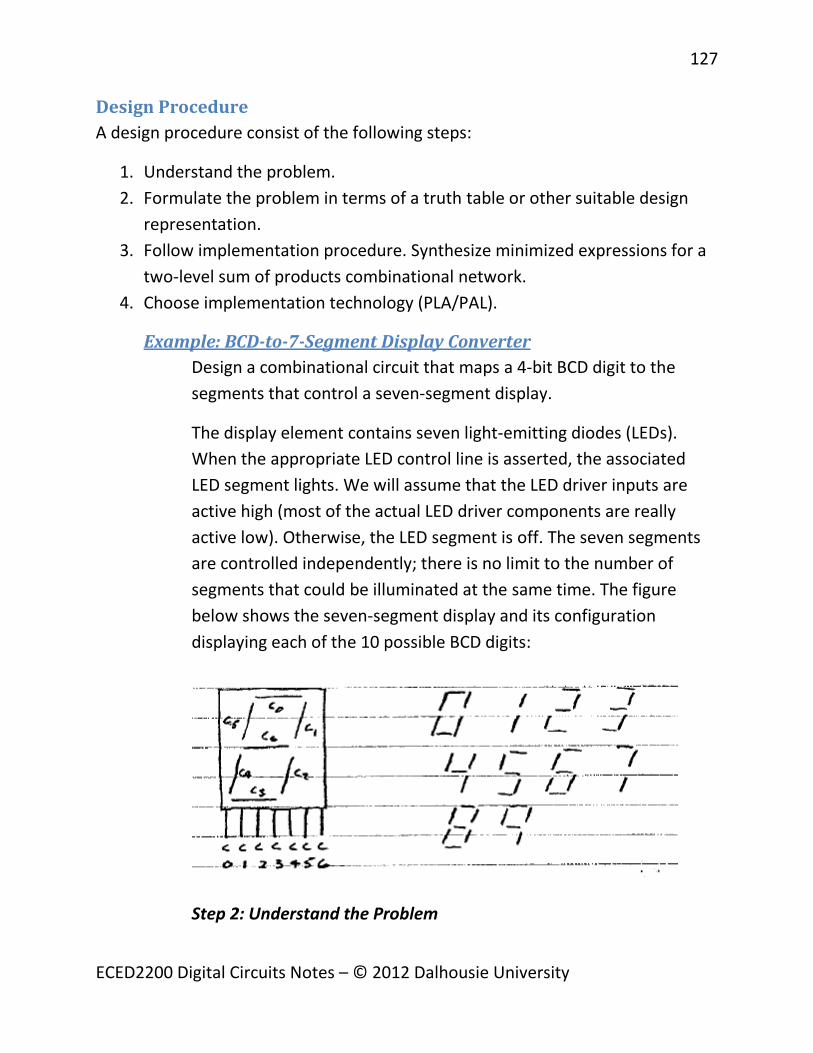
127
ECED2200 Digital Circuits Notes – © 2012 Dalhousie University
Design Procedure A design procedure consist of the following steps:
1. Understand the problem. 2. Formulate the problem in terms of a truth table or other suitable design
representation. 3. Follow implementation procedure. Synthesize minimized expressions for a
two-level sum of products combinational network. 4. Choose implementation technology (PLA/PAL).
Example: BCD-to-7-Segment Display Converter Design a combinational circuit that maps a 4-bit BCD digit to the segments that control a seven-segment display.
The display element contains seven light-emitting diodes (LEDs). When the appropriate LED control line is asserted, the associated LED segment lights. We will assume that the LED driver inputs are active high (most of the actual LED driver components are really active low). Otherwise, the LED segment is off. The seven segments are controlled independently; there is no limit to the number of segments that could be illuminated at the same time. The figure below shows the seven-segment display and its configuration displaying each of the 10 possible BCD digits:
Step 2: Understand the Problem

128
ECED2200 Digital Circuits Notes – © 2012 Dalhousie University
What is the circuit supposed to do? What are the inputs and outputs? There are four input signals, representing the 4-bit BCD digits. There should be seven outputs, one for each of the LED segments that must be controlled. A block diagram is shown below:
Step 2: Formulate in Terms of a Truth Table
It is best to tabulate the input values with the desired outputs. For example, the BCD representation for the digit 0 should cause the LED segment 0,1,2,3,4, and 5 to illuminate. Hence, for the output 0000 the control signals C0 to C5 would be asserted, with C6 unasserted. For the input 0001, segments 1 & 2 are turned on, while segments 0 and 3-6 are left off. In the table entry for 0001, C1 and C2 are asserted, while the remainder are unasserted. The whole truth table is shown below, where the only valid entries are for decimal 0-9, corresponding to binary 0000-1001.

129
ECED2200 Digital Circuits Notes – © 2012 Dalhousie University
Step 3: Implementation Procedure
Since we desire a two-level network we will use K-map techniques. Note that seven 4-variable maps are required. The K-maps with circled prime implicants are shown below:

130
ECED2200 Digital Circuits Notes – © 2012 Dalhousie University
From the K-maps we can write the following equations for the LED segment control outputs:

131
ECED2200 Digital Circuits Notes – © 2012 Dalhousie University
Step 4: Implementation
The PLA implementation is shown below. The limiting factor in a PLA is the number of unique product terms to implement the outputs. There are fifteen required product terms in the above set of equations. A typical PLA component can handle sixteen inputs, eight outputs, and forty-eight product terms. From the K-maps one can see that the hazards are not of concern in this problem. CAD methods can be used to find a multi-level solution.

132
ECED2200 Digital Circuits Notes – © 2012 Dalhousie University

133
ECED2200 Digital Circuits Notes – © 2012 Dalhousie University
Beyond Simple Logic Gates Switching Logic Switching networks provide an alternative to discrete gates for constructing digital systems. They operate by steering or directing inputs to outputs through a network of switching paths rather than by computing a Boolean function.
A typical digital system has several sources of information and several destinations. In practice the desired source is connected to a common path or bus and the bus is then connected to the desired destination. This is called multiplexing and is shown below:
A multiplexor or data selector selects the desired source and places its information on the bus; a demultiplexer or data distributor transfers information on the bus to the selected destination.
Multiplexer/Data Selector A multiplexer, or MUX, is a combinational logic network with 2n data inputs, n control inputs, and one data output. Depending on the settings of the control inputs, a single data input is selected and steered to the outputs. Since a multiplexer selects an input for connection to the output is often referred to as a data selector.

134
ECED2200 Digital Circuits Notes – © 2012 Dalhousie University
The figure below gives a functional truth table in the left and a conventional truth table on the right for a multiplexer with two data inputs, I0 and I1, and one control input A:
The functional truth table indicates that we are passing a selected output to the output. Using a Boolean equation, the two-input multiplexer can be described as:
If A=0, the output is given by I0. If A=1, the output is given by I1.
Multiplexors are described by the number of data inputs, since the number of control inputs can be inferred from this. Hence, a 2:1 multiplexor has two data inputs, one data output, and one control input. A 4:1 multiplexor has four data inputs, one data output, and two control inputs. The figure below shows the block diagrams for 2:1, 4:1, and 8:1 multiplexer:
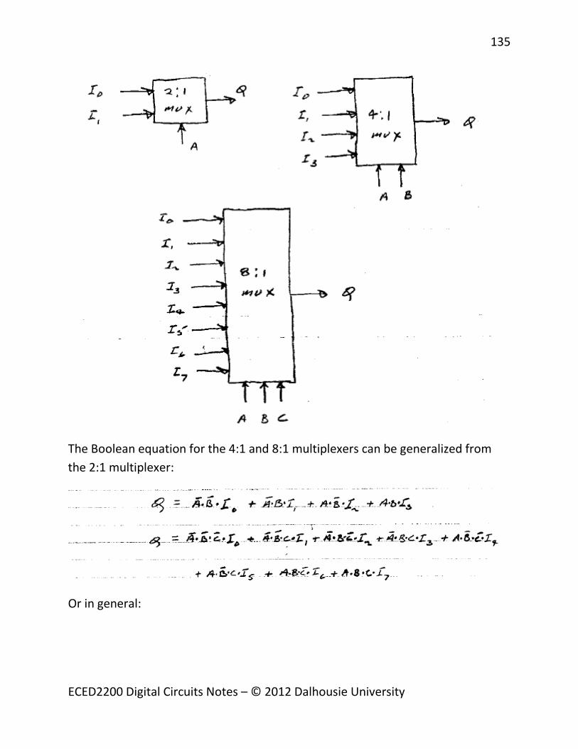
135
ECED2200 Digital Circuits Notes – © 2012 Dalhousie University
The Boolean equation for the 4:1 and 8:1 multiplexers can be generalized from the 2:1 multiplexer:
Or in general:

136
ECED2200 Digital Circuits Notes – © 2012 Dalhousie University
Example: Design a 4:1 multiplexer. Show its block diagram, functional truth table, and logic diagrams. Show how the multiplexer works by considering the case where S1=1, S0=0. Assume the device is enabled, i.e.: E=1.
The block diagram, functional truth table, and logic diagram are shown below:

137
ECED2200 Digital Circuits Notes – © 2012 Dalhousie University
Each of the four inputs I0 through I3 are selected by S0 and S1, and directed to the output when the device is enabled. The equation describing the above device is:
To see how the above device works consider the case where E=1, S0=0, S1=1. Tracing the input signals I0 through I3, we get Q=I2 so only the input whose address equals 2 is seen at the output.
Multiplexer as a Logic Building Block A multiplexer can implement a general-purpose logic building block. A truth table can be implemented directly into hardware by using a multiplexor. Consider the function:

138
ECED2200 Digital Circuits Notes – © 2012 Dalhousie University
The function can be implemented by an 8:1 multiplexer as shown below. The input variables A,B, and C are connected to the multiplexer selection inputs. The input Ii is set to 1 if the function includes minterm mi. All other inputs are set to 0. In this case I0, I2, I6, and I7 are all set to 1, while I1, I3, I4, I5 are set to 0.
To illustrate, consider the case where A=B=C=0. This corresponds to minterm m0. With these inputs the multiplexor will select I0 and set f=1. If A=B=0 and C=1, then I1 is selected and f is set to 0, and so on.
In general, we see that by selecting n-1 variables as control inputs to a 2n-1 input multiplexor, we can implement any Boolean function of a variable.
Example
Use a multiplexer to implement the function f(A,B,C,D) whose k-map is given below.

139
ECED2200 Digital Circuits Notes – © 2012 Dalhousie University
Since f is a function of four variables it can be implemented by an eight-input multiplexer. Select A,B, and C as the control inputs. The k-map is then partitioned into eight pars of k-map entries, each sharing common values for the three control inputs. Each pair can be replaced by either 0,1,D, or NOT D. f can be represented by the equation:
The multiplexer is shown below:

140
ECED2200 Digital Circuits Notes – © 2012 Dalhousie University
Two-, 4-, 8- and 16-to-1 multiplexers are commercially available as MSI packages.
Decoders/Demultiplexer/Data Distribution Decoders convert binary information from one coded form to another. As shown below, the same unit can serve as a decoder or as a demultiplexer (data distributor), depending on how the terminals are interpreted.
When enabled by E going high, the decoder places a 1 on the OUTPUT line corresponding to the INPUT code; all other output lines remain LOW. When used

141
ECED2200 Digital Circuits Notes – © 2012 Dalhousie University
as a demultiplexer DATA from the bus is applied to the E terminal and appears on the DESTINATION line selected by the ADDRESS.
A decoder/demultiplexer takes as input a single data input (an enable signal) and n control signals, and uses the latter to assert one of 2n output lines. For example, a 1:2 decoder/demultiplexer has two inputs, E(enable) and S(select), and two outputs, Q0 and Q1. The Boolean equations for the outputs are as follows:
If E=0 both outputs are at 0. When E=1 the value of S0 determines which of the two outputs will be driven high. The equations for the 2:3 demultiplexer are:
And for the 3:8 demultiplexer:
A decoder/demultiplexer is typically named by the number of control signals and the number of output signals (e.g. 1:2, 2:4, 3:8). Compare with the multiplexer naming: the number of data inputs and the number of data outputs (e.g. 2:1, 4:1, 8:1).
The truth table and logic diagram for a 2:4 demultiplexer are shown below:

142
ECED2200 Digital Circuits Notes – © 2012 Dalhousie University
To see how the input works consider the case where E=1, S1=0, S0=1. Tracing the signals through we see that Q0 Q1 Q2 Q3 = 0100 so that only Q1 receives the data.
Decoder/Demultiplexer as a Logic Building Block A decoder can also be used as a “minterm generator”. The figure below shows a 3:8 decoder where the select lines have signals A,B,C. Each output is labeled with the select line combination that causes that output to be asserted.

143
ECED2200 Digital Circuits Notes – © 2012 Dalhousie University
As an example, suppose the control signals A,B, and C are set to 0,1 and 0,
respectively. This corresponds to minterm and output Q2 is enabled.
The decoder can also be used as a general-purpose combinational logic building block. Any function expressed in sum of products form over n variables can be implemented by an n:2n decoder in conjunction with OR gates.
To illustrate consider the following three functions of the Boolean variables A,B,C,D:
It is more convenient to express as the sum of 4-input minterms:

144
ECED2200 Digital Circuits Notes – © 2012 Dalhousie University
The figure below uses a 4:16 decoder to implement these functions:
f1 is asserted whenever any of its three minterms are asserted. By connection A,B,C, and D to the decoder select lines, the output Q5, Q3, or Q15 will be asserted if the inputs corresponds to the desired minterm. f1 is then implemented by an OR gate connected to these decoder outputs.
In a similar manner, f2 is implemented by a three-input OR gate connected to decoder outputs Q12, Q14, and Q15. f3is obtained by an inverter driven by the Q15 decoder output.
This approach to implementing logic is useful for functions of a relatively small number of variables, as decoders with more than four select inputs are not as readily available, and a small number of minterms per function.

145
ECED2200 Digital Circuits Notes – © 2012 Dalhousie University
Tri-State Gates Besides 0 and 1, there is a third signal value in digital circuits: the high-impedance state, denoted by Z. When a gates output is in a high-impedance state it is as though the gate were disconnected from the output. Gates that can be placed in such a state are called tri-state gates with outputs 0,1, and Z. In addition to its normal inputs, a tri-state has another input called output enable. When this input is 0, the output is Z. When the output enable is 1, the gates output is determined by its data inputs.
The truth table of a tri-state buffer gate is shown below. When output enable (OE) equals 0, the output is Z, no matter what the input A is. When OE=1 the buffer passes its input to the output.
The symbol for the buffer gate is shown below:
Tri-state buffer gates are useful for situations such as a bidirectional data bus, where two drivers are both connected to the same wire. One side must always have their driver in the high-impedance state so the other side can drive the wire.
To see how tri-state gates work, consider the circuit below which consists of two tri-state buffers (with active-high enables) and an inverter:

146
ECED2200 Digital Circuits Notes – © 2012 Dalhousie University
If the Select Input is 0 then I0 steers to f (the output of the I1 buffer is open), and if it is 1 then I1 steers to f (the output of the I0 buffer is open).

147
ECED2200 Digital Circuits Notes – © 2012 Dalhousie University
Sequential Logic Design The basic logic gates are connected to form combinational circuits that make decisions in response to the present inputs. In addition to these decision components we need memory components to store instructions and results. The outputs of these sequential circuits are affected by past inputs as well as present inputs. A memory unit must have the following characteristics:
1. A binary storage device must have two (2) distinct states. 2. It must remain in one state until instructed to change. 3. It must change rapidly from one state to another, and the state value (0 or
1) must be clearly evident.
A simple memory component can be implemented from cascaded inverters. This is the basic circuit structure using in static RAM (Random Access Memory) designs. Alternatively, simple memory structures can be build using cross-coupled NOR or NAND gates. These elements for the basic building blocks of the latch and the flip-flop (bistable multivibrator) memory elements which are used in many types of data processing systems.
Logic Gate Memory Units
Inverter Chains Consider the circuit shown below:
A 1 at the input to the first inverter becomes a 0 at the input to the second which reinforces the value at the first inverters input. Similar a 0 at the input is also reinforced. The circuit is a storage element. Some extra logic is required to open the feedback path what the input is changed:

148
ECED2200 Digital Circuits Notes – © 2012 Dalhousie University
Cascaded inverts can also be used to build circuits whose outputs oscillate between low and high voltages. Such circuits are called ring oscillators. The figure below shows an inverter chain and the associated timing waveform. The waveform begins with A (=X). The odd number of inverters (five) results in a period tp = 10 time units. Duty cycle is defined as the percentage of time a signal is high during its period. In this case the signal has a 50% duty cycle.
In the ring oscillator, the duration of the period depends on the number of inverters in the chain. That that in the example here each inverter has a unit delay.
Cross-Coupled NOR Gates In the NOR gate latch shown below the output of each NOR gate is fed back into the input of the other gate:

149
ECED2200 Digital Circuits Notes – © 2012 Dalhousie University
The operation is summarized in the table below where, to start, we assume the present state of the output Q+ is 0 and the inputs to the set terminal S and the reset terminal R are both 0.
To SET the latch, a 1 is applied to S only. For and
the present state of the output is inconsistent with the input, the

150
ECED2200 Digital Circuits Notes – © 2012 Dalhousie University
systems is unstable, and Q must flip. After Q changes, the present sate changes to
1, and becomes 0, hence =1, a stable state. Note that if either input to a NOR gate is 1, the output is 0. Removing the input from S causes no chance. Hence this is a stable state after being SET. Applying another input to S causes no change.
To RESET the latch, a 1 is applied to R only. This results in an unstable system and must flop to 0. A change in Q to 0 results in a stable output = 0. Removing
the input to R or applying another input to R produces no change. Hence = 0 and =1 is the stable state after being RESET.
Only very short pulses are needed for triggering. Attempting SET and RESET simultaneously would create an ambiguous state with both and = 0. This is unacceptable in a bistable unit and circuits are designed to avoid this condition.
Another way to represent the behavior of a cross-coupled NOR gates is called the state diagram as shown below.
The circuits state depends on the value of Q and NOT Q ( ), so there are four possible states. Since there are two inputs, S and R, there are four transitions for each state.

151
ECED2200 Digital Circuits Notes – © 2012 Dalhousie University
The states 01 and 10 are the normal ones for the circuit. When S=1, we enter state 10 (Q=1, NOT Q = 0). When R=1, the state changes to 01 (Q=0, NOT Q = 1). When S = R = 0 the current state is held.
When S=R=1 the circuit enters the forbidden state 00. It stays as long as those inputs are held. As soon as one input returns to 0, the circuit returns to state 01 or 10. If the current state is 00 and S=R=0, the circuit enters the forbidden state 11. It does not stay very long before returning to state 00 if S and R remain 0. If the delays are match the circuit can oscillate between these states forever. This is known as a race condition. The circuit should never be put in state 00.
From the circuit for the RS latch or the table we can deduce the detailed truth table for the latch as shown below:
Where Q+ is the next state output based on the current state Q and inputs S & R.
The K-map for the truth table is given below:

152
ECED2200 Digital Circuits Notes – © 2012 Dalhousie University
From the K-map we get the characteristic equation:
This equation summarizes the behavior of the RS latch. For example, if S=1 and R=0, the next state Q+ becomes 1 independent of the current state. When S=0 and R=1, the next state is forced to 0, independent of the current state.
Timing Waveforms In the RS latch a 1 input at S will SET the output Q to 1. To RESET the latch, a 1 is applied to input R. The duration of the input (it must exceed a certain minimum time) and the time at which the input signal is applied are not significant. Such a latch responds to the asynchronous inputs.
A more sophisticated latch using two AND gates is shown below.

153
ECED2200 Digital Circuits Notes – © 2012 Dalhousie University
Here an input is effective only when enabled by a 1 input at terminal E. In digital systems composed of many elements, it is usually necessary for the outputs of all elements to be synchronized. The synchronizing signal may come from a clock. The enabling terminal is frequently designed CLOCK (CK). In a clocked system, transactions cannot happen at random by occur in an order one-step-at-a-time fashion. In addition to the synchronous inputs R and S, there may be asynchronous inputs to clear or preset the flip-flops.
Flip-flips different from latches in that their outputs change only with respect to the clock, whereas latches change outputs when their inputs change.
The operation of a clocked RS latch (or flip flop) is shown below. Initially, output Q=0. If a 1 appears at SET, when ENABLE goes to 1 the flip-flop is set with Q=1. At the next clock pulse, the presence of a 1 at RESET forces the output to 0. At any time, a 1 at PRESET forces the output to 1; a 1 input at the CLEAR terminal overrides other inputs and forces Q to 0.
The Data Latch The symbol for a simple RS flip-flop (without PRESET or CLEAR) is shown below. The ambiguous state which results when R=1 and S=1 simultaneously can be avoided by modifying the circuit as shown in (B) below.

154
ECED2200 Digital Circuits Notes – © 2012 Dalhousie University
By connecting an inverter between the R and S terminal and using only one input signal, the ambiguity is avoided and the number of terminals are decreased. When ENABLE is HIGH, the output Q follows the input D, when ENABLE goes LOW, no change in Q is possible, and the output is latched at the previous data value.
This data latch is widely used as an element in digital systems.
Example The enable and data inputs to a data latch are shown below. The product the waveform of the output.
The output Q follows input D whenever enabled (E=1). When E goes to 0, the output remains latched in the previous condition.
In the figure, When E goes HIGH, D=1 so Q follows D and becomes 1. As long as E is HIGH, Q follows any change in D. When E goes LOW, Q=D=1 and remains so. The Q waveform is as shown.

155
ECED2200 Digital Circuits Notes – © 2012 Dalhousie University
The D Flip-Flops Sometimes it is desirable to delay the transfer of data from input to output. For example, we may wish to maintain the present state Q, while a new state is being read that will be transferred later. The D (delay) flip-flop is shown below:
It is a data latch with a second RS flip-flop. The data latch is enabled when the clock signal goes LOW, but the following RS flip-flop is enabled when the clock signal goes HIGH. We see that Q1 follows D whenever CK is LOW, but any change in the output Q=Q2 is delayed until the next upward transition of CK. This is an edge-triggered flip-flop; Q1 follows D while CK is LOW, then on the leading edge of the clock pulse, the value of D is transferred to output Q. On the logic symbol, the small triangle indicates an edge-triggered device.

156
ECED2200 Digital Circuits Notes – © 2012 Dalhousie University
Because the output change only at the instant the clock goes HIGH, the output can be synchronized without the outputs of other elements. In addition, a sudden spurious change in D, like the one shown above, will not affect the output.
The truth table for the D flip-flip is shown below:
The k-maps as obtained from the above table is given below:
From the K-maps we get the characteristic equation:
Timing Timing is more complicated in sequential circuits than in combination circuits where glitches are the only concern. Sequential logic, on the other hand, must examine both the current input & current state to determine the outputs and the next state. In addition, outputs can change in response to clocking changes as well as input changes.
For proper operation the data must be stable for a few nanoseconds before the device is clocked (called the setup time or tsu) and must remain stable for a few

157
ECED2200 Digital Circuits Notes – © 2012 Dalhousie University
nanoseconds after the clocking is initiated (the hold time, th). The figure below shows the timing constraints for a typical edge-triggered flip-flop. In the diagram tw is the clock signal minimum duration, thl is the propagation delay from high to low, and tlh the propagation delay from low to high. Typical numbers are: tw = 25 nS, tsu = 20 nS, th = 5 nS, thl = 25 nS, tlh = 13 nS.
The JK-Flip Flop A very popular memory unit is the JK flip-flop shown below. In its most common form, the output changes state on downward transitions of the clock pulses. The small circle on the symbol identifies this as a falling-edge-triggered flip-flop. The operation is improved by using a master flip-flop that is enabled on the upward transition of the clock pulse while the slave flip-flop is inactive. The slave is enabled on the downward transition and follows its master, i.e. it takes on the state of the master.

158
ECED2200 Digital Circuits Notes – © 2012 Dalhousie University
Because of the feedback connections from the output to the input, the output of the JK flip-flop depends on the state of the inputs and outputs at the instant the clock goes LOW. In addition the ambiguity (R=S=1) is avoided. A truth table showing S1, R1, Q+ (the next output state) for all values of J, K, and Q (the present output state) is shown below:
From the truth table we see the following modes of response are possible:
1. With inputs J=K=0 the clock as no effect, and the flip-flop remains in its present state Q.
2. When J and K unequal, the unit behaves like an RS flip-flop where J=S and K=R. That is J=1 K=0 SETs the output on falling clock edge, and J=0 K=1 RESETS the output on falling clock edge.

159
ECED2200 Digital Circuits Notes – © 2012 Dalhousie University
3. With inputs J=K=1 the flip-flop toggles; that is the output changes each time the clock goes low.
The K-map for the truth table is given below:
From the K-map we get the characteristic equation:
This equation summarizes the behavior of the JK flip-flop.
Example: Two JK flip-flops that respond to downward transitions are connected in tandem as shown. For a 2 KHz square wave input, determine the output:
Since we have 1 inputs at both J and K, the output will change each time the clock goes LOW. For a 2 KHz square wave input the output of the first flip-flop will be a 1 KHz square wave. Since this is the input to the second flip-flop, its output will be 500 Hz.

160
ECED2200 Digital Circuits Notes – © 2012 Dalhousie University
The JK flip-flop is used in a number of digital computer applications such as counters, arithmetic units, and registers. For greater flexibility, some versions include PRESET and CLEAR capabilities as shown below. In the unit shown PR and CLR are normally held HIGH.
The small circles (inversion, or “active low”) indicate that if PR goes LOW, Q is forced to 1; where is CLR goes LOW, Q is forced to 0.
Example Connect a JK flip-flop to function as a data latch. That is, when it is ENABLED, the DATA is to be transferred to Q when clock goes LOW.
Logically this means that: when ENABLED, Q should follow J=D, which requires K is not equal to J. When DISABLED, Q should remain “latched” in its present state, which requires K=J=0. Thus:

161
ECED2200 Digital Circuits Notes – © 2012 Dalhousie University
Which results in the following logic synthesis:
The T Flip-Flop With the J & K inputs tied together (resulting in one terminal), the JK unit becomes the T or toggle flip-flop as shown below:
For T=0 (J=K=0) the clock pulse has no effect on output Q. For T=1 (J=K=1), the flip-flop toggles each time CK goes to LOW. The waveforms shows that for T held HIGH, the output is a square wave of half the frequency of the clock; the device is a frequency divider.
The truth table for a T flip-flop is shown below:

162
ECED2200 Digital Circuits Notes – © 2012 Dalhousie University
The K-map is obtained from the above table and shown below:
Finally from the K-Map we can get the characteristic equation:
Conversion of One Flip-Flop Type to Another Any flip-flop can be implemented as combinational logic for the next state function in conjunction with a flip-flop of another type.
A general procedure to map amount the different kinds of flip-flops is based on the concept of an excitation table. This table lists all possible state transitions and the values of the flip-flop inputs that cause a given transition to take place.
The figure below gives excitation tables for RS, D, JK, and T flip-flops.

163
ECED2200 Digital Circuits Notes – © 2012 Dalhousie University
If the current state is 0 and the next state is to be 0, then the first row of the table describes the flip-flop inputs to cause that state transition to take place. For the RS latch it doesn’t matter the value on R provided that S=0. If using a D flip-flop the input is set to the next discrete state, which is 0 in this case.
If a JK flip-flop us being using, the transition from 0 to 0 occurs when J=0. The value of K does not matter. If using a T flip-flop, the transition does not change the current state, so the input should be 0. The same kind of analysis can be applied to complete the excitation table for the three other cases.
The procedure is to use the excitation table for the flip-flops in question to form a K-map. The K-map layout is for the desired flip-flop and the values entered are for the flip-flops being used. The method is elaborated in the following examples.
Example: JK with D Show how to implement a JK flip-flop starting with a D flip flop.
The excitation table for the JK and D flip-flops are shown below. The K-map is formed for the JK flip-flops with the values for the D flip-flops entered in the map.
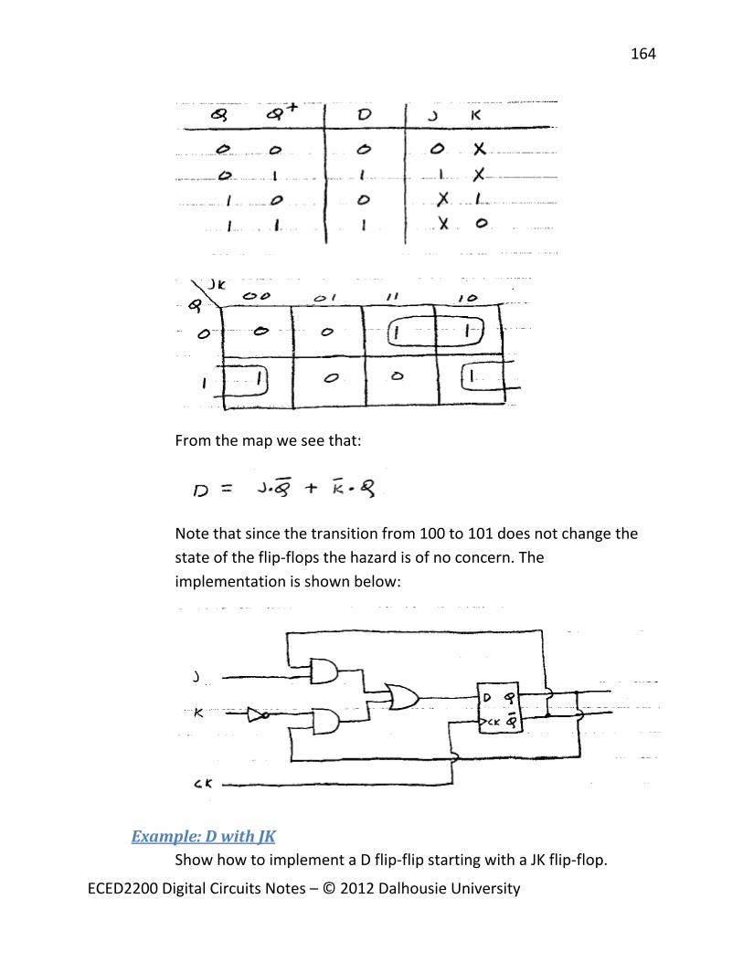
164
ECED2200 Digital Circuits Notes – © 2012 Dalhousie University
From the map we see that:
Note that since the transition from 100 to 101 does not change the state of the flip-flops the hazard is of no concern. The implementation is shown below:
Example: D with JK Show how to implement a D flip-flip starting with a JK flip-flop.

165
ECED2200 Digital Circuits Notes – © 2012 Dalhousie University
The excitation table is as in the last example. The K-maps are formed for the D flip-flops with values for J and K entries in the maps:
From the maps we see that:
Thus the implementation becomes:
Example: RS from JK Implement an RS flip-flop starting with a JK flip-flop.
The excitation table for the RS and JK flip-flops is shown below:

166
ECED2200 Digital Circuits Notes – © 2012 Dalhousie University
The K-maps for the RS are formed from with JK values entered in the maps:
From the K-maps we see that:
Thus:
Example: JK from RS Implement a JK flip-flop starting with a RS flip-flop.
The excitation table for the RS and JK flip-flops is shown below:

167
ECED2200 Digital Circuits Notes – © 2012 Dalhousie University
The K-maps for the JK are formed from with RS values entered in the maps:
We see that:
Thus:
Sets of flip-flops can be used to represent binary numbers in which each digit corresponds to a value of Q (0 or 1) of a flip-flop. A register is a set of flip-flops in

168
ECED2200 Digital Circuits Notes – © 2012 Dalhousie University
which binary data can be stored. Flip-flops can be connected to serve as a counter in which the number stored is the number of events being counted.
Practical Matters Logic gates and memory elements are available in IC form which are small in size, have low power consumption, and have low cost. Typically they are used in DIP (Dual In-line Package), with 14 or 16 pins. A photo of a 14-pin DIP is shown below:
Diagrams for TTL dual D and JK flip-flops are shown below, where the pin numbers correspond to pins on the above package.

169
ECED2200 Digital Circuits Notes – © 2012 Dalhousie University
Debouncing Switches When a switch is flipped from one terminal to another, it does not make a clean, solid contact with the new terminal. Instead, it bounces several times before coming to rest. Because of this and the fact that TTL chips treat floating inputs as 1’s, there are several transitions from 1 to 0. This cause errors in reading the switches output. The following diagram shows an example of switch bounce:
If the switch was for example counting votes, that single push would be read as several quick pushes.
The problem is solved by using an RS latch. The figure below shows an RS latch, a single pole double throw (SPDT) switch, and two resistors connected to ground:

170
ECED2200 Digital Circuits Notes – © 2012 Dalhousie University
When the switch is in the reset position, R is high and Q is low. If the switch is moved so that it is in transition towards S, the grounded resistors pulls the latch low. The latch is in its holding state since both inputs are 0.
When the switch first touches S the latch goes high and Q=1. If the switch bounces, temporarily breaking the connection, the latch input returns to 0, leaving the latch in a holding state. If the switch bounces back, remaking the S connection, the latch is set again and so no state change occurs.
As long as the switch does not bounce enough to remake R, the Q output will remain high as long as the switch is bouncing into its final position.
A similar analysis applies for a switch moving from S to R.
The 555 Timer The 555 timer is a programmable timer chip. The circuit diagram is shown below:

171
ECED2200 Digital Circuits Notes – © 2012 Dalhousie University
The period an duty cycle are determined by placing the appropriate resistors and capacitors between the pins. The following formula are used to calculate the clocks characteristics:
Clock high time = 0.7 (Ra + Rb) C1
Clock low time = 0.7 (Rb) C1
Clock Period = high time + low time = 0.7 (Ra + 2Rb) C1
Clock Frequency = 1 / (Clock Period)
Duty Cycle = (Ra + Rb) / (Ra + 2Rb)
Note that the 555 timer draws large currents for short periods of time when the output changes state. To minimize the resulting spikes that can upset the rest of the circuit it is important to put a 0.1 uF bypass capacitor from the 5V pin, pin 4, to ground.
Example: Design a clock signal with a period of 500 uS and a 75% duty cycle.
Clock frequency = 1/period = 1/500E-6 = 2000 Hz = 2 KHz

172
ECED2200 Digital Circuits Notes – © 2012 Dalhousie University
Sequential Logic Applications In this section we will examine three useful sequential logic components: registers, counters, and memories.
Registers In addition to logic circuits that process data, digital systems must include memory devices to store data and results. A flip-flop can store or “remember” one digit of a binary number, one bit. A register is an array of flip-flops that can temporarily store data or information in digital form. A great variety of registers are available in IC form.
Shift Registers The serial shift register below consists of four trailing-edge-triggered JK flip-flops connected so that J ≠ K. At the trailing edge of each clock pulse Q follows J in each flip-flop of the 4-bit register. The data are entered serially, that is, one bit at a time, and shifted right through the register at each clock pulse.

173
ECED2200 Digital Circuits Notes – © 2012 Dalhousie University
The table below shows how 0100 would be placed in the register:
Begin with the least significant bit. With a 0 at IN=JA and K ≠ J, at the trailing edge of the first clock pulse (CP1), QA follows JA and the LSB is transferred to the output of flip-flop A. During the next clock cycle, B=QA=0 and the second bit, a 1, is applied at IN = JA. At CP2, the 0 is transferred to QB (i.e., shifted one position to the right) and the 1 is transferred to QA. After four clock pulses, the 4-bit number is stored in the register and 0110 is available at parallel outputs ABCD. An

174
ECED2200 Digital Circuits Notes – © 2012 Dalhousie University
application of this register is an serial-to-parallel converter. A single input line and four output lines are required.
The shift register shown below consists of D flip-flops with CLEAR and PRESET. The symbols indicate that the flip-flops are cleared to 0 if CLR goes LOW while PR is inactive (HIGH) (clearing is independent of the clock level). On the positive-going edge of the clock signal, the input at D is transferred to Q.
Since both inputs and outputs are accessible this unit can function as:
i. A 4-bit storage register (serial or parallel) ii. As a serial-to-parallel converter
iii. As a parallel-to-serial converter
For function (iii), all stages are cleared to 0, and the input data are applied to the A,B,C,D INPUTS. A HIGH signal to PRESET ENABLE is NANDed with any 1 input to send PR LOW setting Q to 1 in that stage (independent of the clock level). At the next upward transition of the clock pulse (unless the clock is inhibited), the data are shifted to the right; the value of QD is output and the valued of QC is transferred to QD, etc.

175
ECED2200 Digital Circuits Notes – © 2012 Dalhousie University
A Practical Register The 74173 TTL is a 4-bit register incorporating D flip-flops. The pin diagram is shown below:
For M+N=0, normal logic states are available; for M+N=1, the outputs are disconnected. When both G1 and G2 are LOW, data at the D inputs are loaded on the next positive transition of the CLOCK.

176
ECED2200 Digital Circuits Notes – © 2012 Dalhousie University
Counters Flip-flops can be connected as counters to count random events, or to divide a frequency or to measure a parameter (e.g.: time, distance, speed).
Counters are used to keep track of operations in digital computers and in instrumentation. JK, T and D flip-flops are used in counter design.
Types of Counters
Divide-by-n Circuits A divide-by-n counter produces one output pulse for n input pulses: n is called the “modulo” of the counter. As we see earlier a J-K flip-flop divides by two or four for J&K help HIGH, the output Q is the number of CK inputs divided by two.
Two D flip-flops can be used to obtain a divide-by-four circuit as shown below:

177
ECED2200 Digital Circuits Notes – © 2012 Dalhousie University
With QA and QB cleared (0), when clock sign f goes LOW, CK goes HIGH and DA =
AQ = 1 is transferred to QA. The next time f goes LOW, QA changes to low; time cycles at f complete one cycle of QA, or QA=f/2. When QA goes low, A BQ CK= goes
HIGH and BBD =Q =1is transferred to BQ ; from cycles at f complete one cycle of BQ or BQ = f/4.
Binary Ripple Counter The counter shown below shows a 3-bit ripple counter using JK flip-flops in cascade. With J and K held HIGH (the +5V connections are not shown), the flip-flops toggle at each downward transition of the pulse at CK. The bit QA changes state after each input pulse goes low. The next bit QB changes state whenever QA goes LOW since QA supplies CKB. Similarly, QC changes state whenever QB goes LOW.

178
ECED2200 Digital Circuits Notes – © 2012 Dalhousie University
The table below shows the outputs QA, QB and QC for the first 8 clock pulses. Note that this counter is counting from 000 to 111. After the count reaches 111, counting begins again from 000. Thus, a 3-bit counter cycles through 8 states 000 through 111. Similarly, a 4-bit counter will cycle through 16 states, 0000 through 1111. In general, an n-bit ripple counter will cycle through 2n states, 0 through 2n-1.

179
ECED2200 Digital Circuits Notes – © 2012 Dalhousie University
Counters that cycle through 2n states, from 0 to 2n-1, are known as up-counters. In some cases it is desirable to counter down, and the circuits are known as down-counters. An n-bit ripple counter that cycles through the 2n states is known as a divide-by-2n counter or as a modulo-2n binary counter.
The present unit is an asynchronous binary, modulo-8, ripple counter; asynchronous because all flip-flops do not change at the same time; binary because it follows the binary number sequence with bit values 20, 21, and 22; modulo-8 because it counts through 8 distinct states; ripple because the changes in state ripple through the stages.
Example Design a modulo-5 binary counter using T flip-flops with CLEAR capability.
Three stages are required to counter beyond 4. A modulo-5 counter must counter up to 4 and then, on the fifth pulse, clear all flip-flops to 0. The truth table is shown below:

180
ECED2200 Digital Circuits Notes – © 2012 Dalhousie University
At the count of 5, the 1’s at QA and QC can be NANDed. To generate a CLEAR signal as shown below:
Decade Counters Communication with humans is more convenient in the decimal system. Flip-flops count in binary so binary numbers must be coded in decimal. To counter to 10 in the 8-4-2-1 code, four flip-flops are required. Ten distinct states can be obtained by modifying a 4-bit binary counter so that it skips the last six states. At counts in a normal manner from 0 to 9, then feedback logic resets the next count to zero.
Example Design an 8-4-2-1 BCD ripple counter as follows:
A. Draw a block diagram of a 4-stage binary ripple counter using T flip-flops ABCD (T held HIGH).
B. Show the truth table of flip-flops for a decade counter that counts normally to decimal 9 and then resets to 0000. How

181
ECED2200 Digital Circuits Notes – © 2012 Dalhousie University
does it differ from the truth table for a binary counter in the tenth row?
C. Modifying the circuit to accomplish the following: On the eighth count, the change in state of the D (MSB) flip-flop is to disable the input to the B flip-flop so it will not change or counter to 10. (see part (D)).
D. Modify the circuit so that on the tenth counter flip-flop D will be reset to 0 by the output of A flip-flop, without affecting the use of QC to toggle D.
E. Check the operation of the decade counter by drawing CK and flip-flop waveforms.
The results are as follows:
1. The block diagram is shown below:
2. The truth table is shown below. Note that in the tenth row the counter is set to 0000, whereas the binary counter would have 1010 in that row.

182
ECED2200 Digital Circuits Notes – © 2012 Dalhousie University
3.
4.
5. The waveforms are shown below:

183
ECED2200 Digital Circuits Notes – © 2012 Dalhousie University
Synchronous Counters One disadvantage of ripple counters is the slow speed of operation caused by the long time required for changes in state to ripple through the flip-flops. In addition these time delays can cause temporary state combinations (and voltage spikes called glitches) that result in false synchronous counters in which all flip-flops change state at the same instant.
In the synchronous counter shown below, T flip-flop A toggles, and the other flip-flops are clocked. Flip-flop B toggles on the next counter after QA becomes 1, as shown in the truth table. The AND gate causes flip-flop C to toggle on the next counter after QA and QB = 1 as called for in the truth table.

184
ECED2200 Digital Circuits Notes – © 2012 Dalhousie University
In general, synchronous counters are fast and trouble free.
Ring Counters The figure below shows a 4-bit ring counter using D flip-flops. As in a synchronous counter, all flip-flops are triggered simultaneously; however, the output of each flip-flop drives only the adjacent flip-flops. In a ring counter a single pulse propagates through the ring, while all remaining flip-flops are at the zero-state.

185
ECED2200 Digital Circuits Notes – © 2012 Dalhousie University
The truth table is shown below:
A modulo-N ring counter requires N flip-flops and no other gates.
Counter Design Procedure Counters are the simplest possible finite-state machines. The typically have only a single input instructing them to counter (after just the clock), and their outputs are just the current state.
A generalizing design process consists of the following four steps:
1. From the written specifications of the counter draw a state transition diagram that shows the counters desired sequence.

186
ECED2200 Digital Circuits Notes – © 2012 Dalhousie University
2. Design the state transition table from the state diagram, tabulating the current stat with the next state in the count sequence. Each state-bit is implemented by its own flip-flop.
3. Express each next-state bit as a combinational logic function of the current state bits.
4. Choose a flip-flop for implementation of “remap” the next-state mapping (K-maps) determined in step 3 to obtain the desired behavior from the selected flip-flop.
Example: Generalized Counter Design Design a 3-bit counter that advances through the sequence 000,010,011,101,110,000 and repeats. Not all the possible combinations of the 3 bits represent a valid state. The unused states 001,100, and 111, can be used as don’t care conditions to simplify the logic.
A. The state transition diagram is shown below:

187
ECED2200 Digital Circuits Notes – © 2012 Dalhousie University
B. The state transition table is shown below. Note, the storage elements are named CBA.
C. To express each next-state bit as a combinational logic function of the three current-state bits we draw the K-maps as shown below.

188
ECED2200 Digital Circuits Notes – © 2012 Dalhousie University
D. Since this is almost a straight binary sequence we will use a T flip-flops. The T flip-flops excitation table shown below will be used to derive new next state K-maps:
The figure below shows the toggle inputs needed to implement the desired state transitions:
For example, counter state 000 advances to 010, so the T inputs should be 0 (don’t toggle) for C, 1 (toggle) for B, and 0 (don’t toggle) for A. Similarly, state 110 returns to 000. In this

189
ECED2200 Digital Circuits Notes – © 2012 Dalhousie University
case, the control for C, B, A is toggle, toggle, don’t toggle respectively, or 110.
The remapped K-maps for toggle implementation are given below:
Using the K-maps we obtain the minimalized functions:

190
ECED2200 Digital Circuits Notes – © 2012 Dalhousie University
The implementation is shown in the figure below. To reduce wiring complexity, the input and output networks are labeled rather than drawn as wires. Two networks with the same label are understood to be connected.
The timing waveform is also shown below. The proper sequencing through the states 000, 010, 011, 101, 110, 000 is clear from the waveform.

191
ECED2200 Digital Circuits Notes – © 2012 Dalhousie University
Self-Starting Counters The counter should never be assumed to start in a particular state unless it is designed to do so. At power up the states are undefined; they could be 0 or 1 at random.
This leads to a problem for counters that do not use all state combinations of the storage elements. What happens if a counter enters one of the unused states at start-up depends on how don’t cares have been mapped into 0’s and 1’s by the implementation procedure. The counter could sequence through the non-counter states and never enter the sequence it was designed for.
Verifying if a Counter is Self-Starting A self-starting counter is one in which every possible state, even those not in the desired counter sequence, has a sequence of transitions that eventually leads to a valid counter state. Therefore, no matter how the counter starts up, it will eventually enter the proper counter sequence.
In general, it is desirable to enter the counter sequence is as few transitions as possible. However, it may be an advantage to depart from this rule if the sequence of noncounter states leads to reduced hardware.
A procedure to check if the counter is self-starting is illustrated in the following example.

192
ECED2200 Digital Circuits Notes – © 2012 Dalhousie University
Example Analyze the solution of the last example to check whether or not it is self-starting.
First, replace the don’t cares in the K-maps for the toggle implementation of the last example with the actually assigned 1’s and 0’s (they are underlined in the figure below):
Since the K-maps represent the inputs to the toggle flip-flops they will be used to determine the flip-flops next state as shown in the diagram below. The next state is determined from the present state and the toggle inputs as required by the toggle excitation table.

193
ECED2200 Digital Circuits Notes – © 2012 Dalhousie University
The complete state transition diagram as obtained from the table is shown below. Note the counter is self-starting. It may however require two transitions before it is in the correct sequence.
Counter Reset In the last example the particular starting state did not matter. It is more usual to have a fixed starting state for the counter or finite-state machine.

194
ECED2200 Digital Circuits Notes – © 2012 Dalhousie University
Flip-flops typically have preset and clear inputs. By use of those inputs any state can be chosen as the starting state.
Implementation with Different Kinds of Flip-Flops Toggle flip-flops are a natural choice for implementing binary counters, but other flip-flop types may need less hardware for implementation.
We have shown how to implement the finite-state up-counter using toggle flip-flops. We will now implement this counter using RS, JK, and D flip-flops.
Example Implementation with RS Flip-Flops Implement the five-state up-counter of the earlier example using RS flip-flops.
The first two steps of the counter design procedure – the state transition diagram, the state transition table, and the next-state K-map have already been performed. The next step starts with the RS flip-flop excitation table as shown below:
This table will be used to determine the RS inputs needed to implement the desired state transitions, as shown in the figure below.

195
ECED2200 Digital Circuits Notes – © 2012 Dalhousie University
The re-mapped K-maps for the RS implementation are given below.
Using the K-maps we obtain the minimized functions:

196
ECED2200 Digital Circuits Notes – © 2012 Dalhousie University
The implementation is shown in the diagram below. The figure doesn’t show the reset logic.
To check if the system is self-starting we replace the don’t care in the K maps with the actually assigned 1’s and 0’s (see table below):

197
ECED2200 Digital Circuits Notes – © 2012 Dalhousie University
The complete state transition diagram as obtained from the table is shown below. Note that the counter is self-starting. It may take three transitions before reaching the correct sequence.
Example Implementation with JK Flip-Flops Implement the five-state up-counter of the earlier example using JK flip-flops.

198
ECED2200 Digital Circuits Notes – © 2012 Dalhousie University
As in the last example the first three steps of the design procedure have been performed. The last step starts with the JK flip-flops excitation table as shown below.
From this table the JK inputs needed to implement the desired state transition will be determined (see table below).
The remapped K-maps for the JK implementation are given below.

199
ECED2200 Digital Circuits Notes – © 2012 Dalhousie University
Using the K-maps we obtain the minimized functions:
The implementation is shown in the diagram below. Again the reset logic is not shown.

200
ECED2200 Digital Circuits Notes – © 2012 Dalhousie University
To check if the system is self-starting we replace the don’t cares in the K-maps with the actually assigned 1’s and 0’s (see table below).
The complete state transition diagram as obtained from the table is shown below. Note that the counter is self-starting. If may take three transitions before reaching the correct sequence.

201
ECED2200 Digital Circuits Notes – © 2012 Dalhousie University
Example Implementation with D Flip-Flops Implement the five-state up-counter of the earlier example using D flip-flops.
Again as in the last example the first three steps of the design procedure have been performed. From the excitation table for the D flip-flops shown below it is seen that the D inputs are identical to the next-state outputs.
These are already tabled in the state transition table. We place the next state outputs into K-maps and find the minimized functions. The K-maps are identical to those obtained earlier in the original example.

202
ECED2200 Digital Circuits Notes – © 2012 Dalhousie University
Using the K-maps we obtain the minimized functions:
The implementation is shown in the diagram below. The reset logic is not shown.

203
ECED2200 Digital Circuits Notes – © 2012 Dalhousie University
To check if the system is self-starting we replace the don’t cares in the K-maps with the actually assigned 1’s and 0’s:
The complete state transition diagram as obtained from the table is shown below. Note that the counter is self-starting. It may take two transitions before reaching the correct sequence.
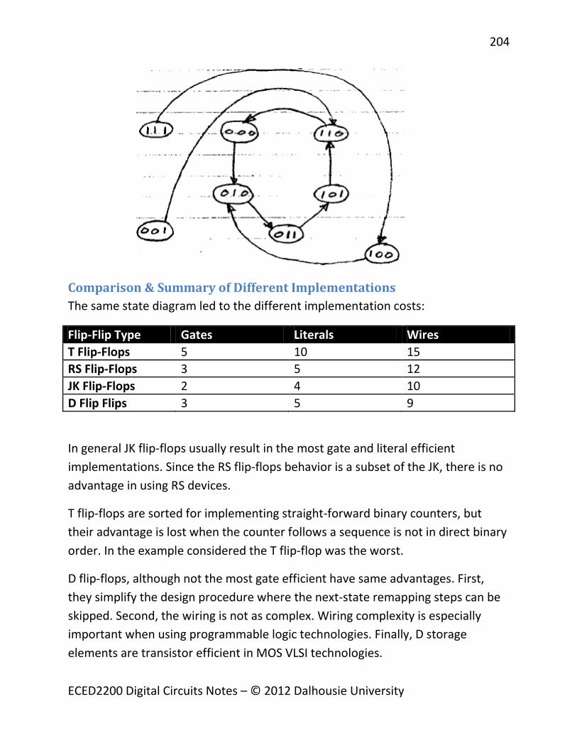
204
ECED2200 Digital Circuits Notes – © 2012 Dalhousie University
Comparison & Summary of Different Implementations The same state diagram led to the different implementation costs:
Flip-Flip Type Gates Literals Wires T Flip-Flops 5 10 15 RS Flip-Flops 3 5 12 JK Flip-Flops 2 4 10 D Flip Flips 3 5 9
In general JK flip-flops usually result in the most gate and literal efficient implementations. Since the RS flip-flops behavior is a subset of the JK, there is no advantage in using RS devices.
T flip-flops are sorted for implementing straight-forward binary counters, but their advantage is lost when the counter follows a sequence is not in direct binary order. In the example considered the T flip-flop was the worst.
D flip-flops, although not the most gate efficient have same advantages. First, they simplify the design procedure where the next-state remapping steps can be skipped. Second, the wiring is not as complex. Wiring complexity is especially important when using programmable logic technologies. Finally, D storage elements are transistor efficient in MOS VLSI technologies.

205
ECED2200 Digital Circuits Notes – © 2012 Dalhousie University
In summary, for conventional packaged MSI/SSI TTL designs, JK flip-flops are usually preferred, especially when the design criterion is minimum gate and literal count. D-type devices are preferred when designing with programmable logic or in more highly integrated technologies than TTL, where minimum wire count or simplified design procedure is the objective.
The technique we have been discussing can be used in a reverse order to obtain the state transition table and diagram when the final circuit implementation is given.
Example Find the state transition table and counter state diagram for the implementation given below.
From the above diagram we see that:

206
ECED2200 Digital Circuits Notes – © 2012 Dalhousie University
We can now use the above expression along with the excitation table for the JK flip-flop to obtain the state transition table.
The state transition diagram is given below:
From the above diagram we see that two of the eight counts are not part of the counter sequence. However, since 111 -> 000 and 011 -> 100 the counter is self-starting.
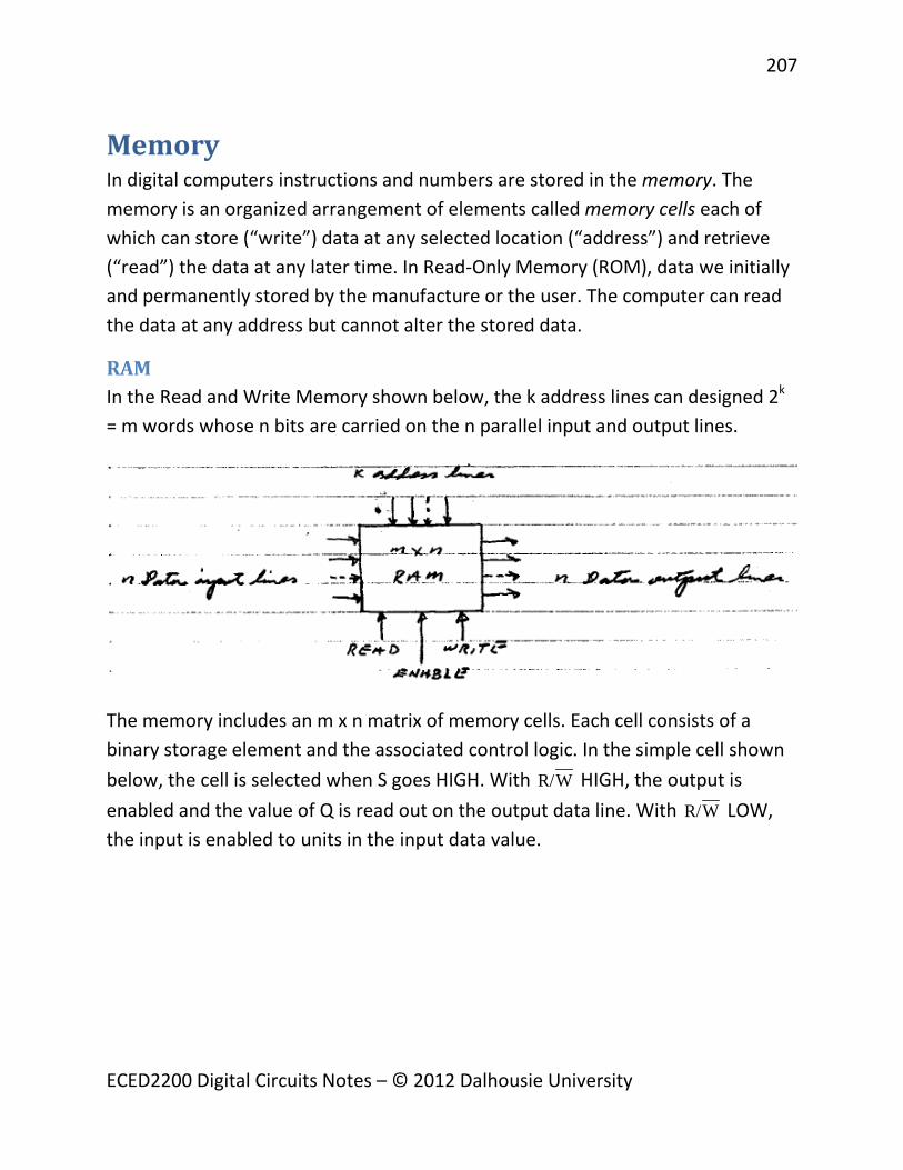
207
ECED2200 Digital Circuits Notes – © 2012 Dalhousie University
Memory In digital computers instructions and numbers are stored in the memory. The memory is an organized arrangement of elements called memory cells each of which can store (“write”) data at any selected location (“address”) and retrieve (“read”) the data at any later time. In Read-Only Memory (ROM), data we initially and permanently stored by the manufacture or the user. The computer can read the data at any address but cannot alter the stored data.
RAM In the Read and Write Memory shown below, the k address lines can designed 2k = m words whose n bits are carried on the n parallel input and output lines.
The memory includes an m x n matrix of memory cells. Each cell consists of a binary storage element and the associated control logic. In the simple cell shown below, the cell is selected when S goes HIGH. With R/W HIGH, the output is enabled and the value of Q is read out on the output data line. With R/W LOW, the input is enabled to units in the input data value.

208
ECED2200 Digital Circuits Notes – © 2012 Dalhousie University
An example of an elementary RAM with a capacitor of two 3-bit words is shown below:
The address causes the decoder to activate one of the two word-select lines. In the WRITE operation ( R/W LOW), 3 bits of data are transformed from the input lines to the selected word. In the READ operation the 3 bits of the selected word

209
ECED2200 Digital Circuits Notes – © 2012 Dalhousie University
are transferred to the output lines with the OR gates. The outputs of the unselected words are all LOW.
Because the words in memory can be accessed in any order, we have a Random-Access Memory (RAM). In the 2x3 RAM above, address selection is linear, since one word-select line is activated. In large memories, selection is coincident since each cell is accessed by addressing an X select line to select the row and a Y select line to select the column. The intersection of the X and Y lines gives one cell in a two-dimensional matrix.
There are two types of RAM, static and dynamic. SRAM retains its data as long as power is applied without any further action from the computer. Each cell of a static RAM is a flip-flop. DRAM requires continuous actions from the computer to maintain its contents. Each cell in a dynamic RAM is a capacitor, which leaks charge and therefor requires continuous recharging to maintain its value. SRAM is used in microprocessor based systems that require small memory; DRAM is used in large memory systems because of lower cost and greater density.
MOS devices are widely used because of their high packing density and low power consumption. Bipolar RAM’s are very fast but are less compact and less energy efficient than MOS RAM’s. They are used as a “scratch-pad” memory for data being processed.
Example An array of eight memory cells is arrange in two rows and four columns. Design he addressing system consisting of a row decoder and a column decoder. Assume a row or column is selected when driven HIGH (logic 1).
A) Row 0 and 1 are selected by row-select (RS) values 0 and 1 and columns 0 to 3 are selected similarly. Compare the truth tables for RS and for CS1 and CS2.
B) Show the eight memory cells (lettered A through D and E through H). Design the decoders using AND and NOT gates only and show the two decoder circuits on your diagram.

210
ECED2200 Digital Circuits Notes – © 2012 Dalhousie University
C) Specify the address values that will select cell F.
D) How many row-select and column-select lines would be required to address 1024 cells arranged in 16 rows and 64 columns.
Answers:
A) The truth tables are shown below:

211
ECED2200 Digital Circuits Notes – © 2012 Dalhousie University
B)
C) Cell F is selected when:
RS = 1; CS1 = 0; CS2 = 1
D) The number of rows/columns is given by:
Number of rows/columns = 2k
Where k = number of rows/columns select lines
So 16 rows = 24, which means 4 row select lines are required.
So 64 columns = 26, which means 6 column select lines are required.
ROM In Read-Only Memory (ROM), binary data is physically and permanently stored by deforming the state of the memory cells. A set of input signals on the address

212
ECED2200 Digital Circuits Notes – © 2012 Dalhousie University
lines is decoded to access a given set of cells whose states then appear on the output lines.
A typical 4x16 ROM is shown below:
The 64 bits of the 4x16 ROM are stored in 64 memory cells arranged in 2k = 22 = 4 words of 16 bits each available at the 16 output lines. The address is coded as a K-bit binary number; a decoder translates the coded address and specifies one of the 2k words. On the 2x4 decoder shown below, the address xy = 10 yields a 1 at D2 ( xy ) and specifies that word 2 is to be read, that is, connected to the 16 output lines.

213
ECED2200 Digital Circuits Notes – © 2012 Dalhousie University
The function performed can be described as follows: (1) If the input is an address and the output is a word (data or instructions) stored, we have a “memory”. (2) If the input is data coded in one form and the output is the same data coded in another form we have a “code converter”. (3) If the input is a set of binary variables (a binary function) and the output is a related binary function we have a “combinational logic circuit” that can replace a network of logic gates.
There are three types of read only memory; mask-programmable (ROM), programmable (PROM), and erasable programmable (EPROM). The masked-programmed ROM’s are programmed during manufacturing. A PROM device initially contains all 0’s; the user programs the unit by electrically changing appropriate 0s and 1s. This is an irreversible process. EPROMs can be programmed and erased repeatedly. EPROMs can be erased by shining and ultraviolet light into a window at the top of the device.
The same bipolar and MOS technologies are used in IC ROM as in RAM. In general ROM is simpler since fewer control elements are necessary and no provision is made for changing cell states.
Example Show how a ROM can be used to realize:
A) The multiplexer discussed earlier, 4:1 MUX
B) The decoder discussed earlier, 2:4 DEC
Answers:
A) For each combination of values at the E, I0, E1, I2, I3, S1, and S0 inputs, the output is to be 0 or 1. If each input combination is considered as an “address”, a ROM can store all possible outputs. For these 7 inputs, a 27 = 128x1 ROM is needed. A few representative lines of the truth table are given below.

214
ECED2200 Digital Circuits Notes – © 2012 Dalhousie University
Connect E, I0, E1, I2, I3, S1, and S0 to the address inputs as shown below.
B) For this case 32 bits of ROM (8x4) are needed. Connect E, S1 and S0 to the address lines, and the 4 output lines to the destination (Q0, Q1, Q2, Q3). The outputs will all be 0 whenever E=0. The truth table for the decoder as given before is reproduced here:

215
ECED2200 Digital Circuits Notes – © 2012 Dalhousie University
Connect E, S1 and S0 to the address lines as shown below:

216
ECED2200 Digital Circuits Notes – © 2012 Dalhousie University
Finite State Machines Finite state machine are so named because the sequential logic that implements them can be in only a finite number of possible states. The counters discussed earlier are simple finite state machines. Their outputs and states are identified, and there is no choice of the sequence of counting.
In the more generalized case, the outputs and next state of the finite state machine are combinational logic functions of their inputs and present state. Finite state machines are essential for realizing the control and decision-making logic in digital systems.
In designing finite state machines a rigorous synchronous design methodology will be followed. This means that the state changes will be toggled with a global reference signal, the clock. State time is defined as the time between related clocking events.
Finite State Machine Design Procedure A general design procedure for arbitrary finite state machines is given below.
1) Understand the problem. A finite state machine is often described by a written specification of its behavior. Some input sequences should be tried to help understand the conditions under which the various outputs are generated. Outcome: Descriptive block diagram
2) Obtain an abstract representation of the FSM. Put the problem in a form that is easy to manipulate by known procedures (e.g.: draw a state diagram). Outcome: Initial State Diagram
3) Perform state minimization. The abstract representation after has too many states. Some states may be eliminated to simplify the problem. Outcome: Simplified State Diagram & Symbolic State Transition Table

217
ECED2200 Digital Circuits Notes – © 2012 Dalhousie University
4) Perform state assignment. Outputs are derived from present and past
states and a good choice of how to encode the state after leads to a simple implementation. Outcome: Encoded State & Transition Table
5) Choose flip-flop types for implementing the FSM’s state. JK flip-flops tend to reduce gate count but have more connections. D flip-flops simplify the connection process.
6) Implement the finite state machine. Using Boolean equations or K-maps for the next state and output combinational functions produce the minimized two-level or multilevel implementations. Outcome: Remapped state transition Table (using excitation table of flip-flops), K-maps for flip-flop inputs & FSM output, Circuit Synthesis
Example: A Simple Vending Machine Implement a simple finite state machine that controls a vending machine.
The control works as follows: The vending machine delivers a package of gum after it has received 15 cents in coins. The machine has a single coin slot that accepts nickels and dimes, one coin at a time. A mechanical sensor indicates to the control whether a dime or a nickel has been inserted into the coin slot. The controller’s output causes a single package of gum to be released down a chute to the machine is to be designed so it does not give change. A customer who uses two dimes losses 5 cents.
1) Draw a block diagram to understand the inputs and outputs. In the figure below N is asserted for one clock period when a nickel is inserted into the coin slot:

218
ECED2200 Digital Circuits Notes – © 2012 Dalhousie University
D is asserted when a dime has been deposited. The machine asserts Open for one clock period when 15 cents (or more) has been deposited since the last reset. It will be assumed that the coin sensor returns any coin not recognized, leaving N and D unasserted, and that extreme logic resets the machine after the gum is delivered.
2) A more suitable abstract representation is obtained by enumerating the possible unique sequences of inputs or configurations of the system. For this case gum is released for the input sequences:
• Three nickels in sequence: N, N, N
• Two nickels followed by a dime: N, N, D
• A nickeled followed by a dime: N, D
• A dime followed by a nickel: D, N
• Two dimes in sequence: D, D
This can be represented as a state diagram as shown below.

219
ECED2200 Digital Circuits Notes – © 2012 Dalhousie University
To keep the state diagram simple only transitions that explicitly cause a state change are concluded. Also Open is shown only in states where it is asserted.
3) This nine-state description is not the best. Since states S4, S5, S6, S6, and S8 have identical behavior they can be combined into a single state.
A further reduction can be obtained if we think of each state as representing the amount of money received so far. The state diagram derived in this way is shown below. Note that only four states are required:

220
ECED2200 Digital Circuits Notes – © 2012 Dalhousie University
Techniques are available for minimizing the number of states. We now have a finite state machine with a minimum number of states. The symbolic state transition table is shown below. Note we assume that N and D are never asserted at the same time.
4) Next the states must be encoded. A natural state assignment would encode the states in 2 bits: state 0₵ as 00, state 5₵ as 01, state 10₵ as 10 and state 15₵ as 11. The encoded state transition table is shown below. A number of computer-based tools are available for funding an effective state encoding.

221
ECED2200 Digital Circuits Notes – © 2012 Dalhousie University

222
ECED2200 Digital Circuits Notes – © 2012 Dalhousie University
5) Implementation based on both D and JK flip-flops will be considered.
6) The K-maps for the D flip-flops implementation are shown below. These maps are obtained directly from the encoded state transition table.

223
ECED2200 Digital Circuits Notes – © 2012 Dalhousie University
From the K-maps we obtain the following minimized equations:
The logic circuit is shown below. It uses eight gates and two flip-flops.

224
ECED2200 Digital Circuits Notes – © 2012 Dalhousie University
To implement using JK flip-flops the next-state functions must be remapped. We start with the JK excitation table as shown below:
The remapped state transition table is shown below.

225
ECED2200 Digital Circuits Notes – © 2012 Dalhousie University
The remapped K-maps for the JK implementation are given below.

226
ECED2200 Digital Circuits Notes – © 2012 Dalhousie University
Using these K-maps we obtain the minimized functions:
The implementation is shown below, it requires six gates and two flip-flops. This is a slight improvement over the D flip-flop case.

227
ECED2200 Digital Circuits Notes – © 2012 Dalhousie University
Moore and Mealy Machines The most general form of a sequential circuit has inputs, outputs, and internal states. It is customary to distinguish between two types of sequential circuits: the Moore machine and the Mealy machine.
The Moor Machine In the Moore machine, the outputs are a function of the present state only. An example of a Moore machine is shown below.
The circuit can be specified by the following input functions:

228
ECED2200 Digital Circuits Notes – © 2012 Dalhousie University
We see that the outputs are taken from the flip-flops and are a function of the present state only. The outputs change synchronously with the state transition and the clock edge. The finite state machine we have considered so far are Moore machines.
For the given system we can use the JK excitation table to find the state table and state transition diagram.
The state transition table is given below:
The state transition diagram is shown below:

229
ECED2200 Digital Circuits Notes – © 2012 Dalhousie University
Note that since the directed lines are marked with a single binary digit without a slash, there is one input variable and no output variables. The state of the flip-flops may be considered the outputs of the circuit.
The Mealy Machine In the Mealy machine, the outputs are functions of both the present state and inputs. An example of a Mealy machine is shown below. The circuit has one input x, one output y, and two D flip-flops A and B. The logic diagram can be expressed algebraically with two flip-flop input functions and one output circuit function:

230
ECED2200 Digital Circuits Notes – © 2012 Dalhousie University
We see that the output Y is a function of both input X and the present state of A and B. The outputs can change immediately after a change at the inputs, independent of the clock. A Mealy machine constructed in this fashion has asynchronous outputs.
For the given system we can use the D excitation table to find the state table and the state transition diagram.

231
ECED2200 Digital Circuits Notes – © 2012 Dalhousie University
Note that D=Q+
The state transition table is given below:
The state transition diagram is shown below:

232
ECED2200 Digital Circuits Notes – © 2012 Dalhousie University
Note that the labeling on the directed lines indicate the input and output variables (i.e.: i/o = input/output).
An example where we obtain the circuit diagram gives the state transition diagram, inputs and outputs is given below.
Example: A sequential circuit has three flip-flops, A, B, C; one input, x; and one output, y. The state diagram is shown below. The circuit is to be designed by treating the unused states as don’t care conditions. Check the final circuit to ensure that it is self-starting. Use JK flip-flops in the design.
From the given diagram and the excitation table for JK flip-flops we can obtain the state table as given below.

233
ECED2200 Digital Circuits Notes – © 2012 Dalhousie University
From the above table we can obtain the K-maps:

234
ECED2200 Digital Circuits Notes – © 2012 Dalhousie University
Using the K-maps we obtain the minimized functions:
The implementation is shown below:

235
ECED2200 Digital Circuits Notes – © 2012 Dalhousie University
Note that the shorthand notation is used in the above diagram so that leads with the same label are connected together.
Since the state 101, 110, and 111 are not used the circuit must be checked to ensure that it is self-starting. To check we see what the don’t cares become in the K-maps. The results are shown by the

236
ECED2200 Digital Circuits Notes – © 2012 Dalhousie University
numbers next to the X’s and the state transition table. The complete state transition diagram is shown below.
We see from the last diagram that the system is self-starting.
Alternative State Machine Representations State diagrams do not adequately capture the notion of an algorithm and are ineffective at capturing the structure behind complex sequencing. As a result hardware designers have shifted toward using alternative representations of FSM behavior that resemble software descriptions. The following alternate representations are being used:
A) Algorithmic state machine (ASM) notation, which is similar to program flowcharts but has a more rigorous concept of timing
B) Hardware Description Languages (HDLs), which look like programming languages, but they explicitly support parallel computations.