digital circuits 3: combinational circuits · digital circuits 3: ... adders and subtractors...
TRANSCRIPT
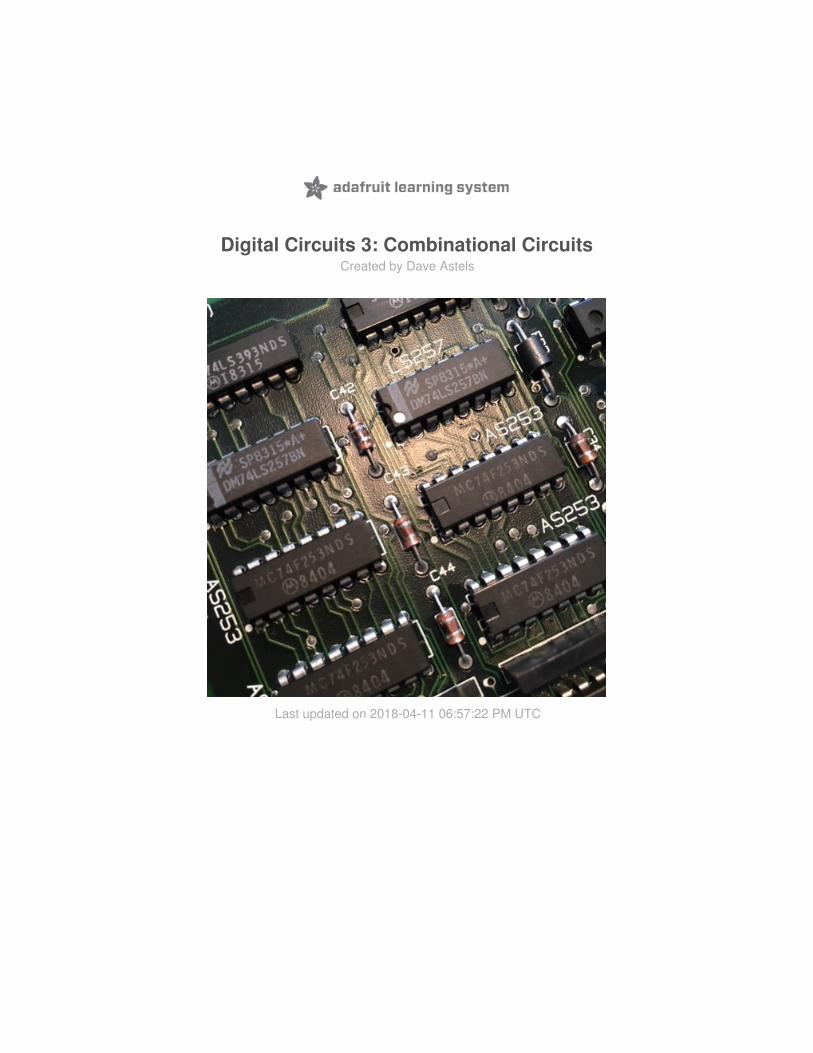
Digital Circuits 3: Combinational CircuitsCreated by Dave Astels
Last updated on 2018-04-11 06:57:22 PM UTC
23444
8888
1010101113141616
1719
Guide Contents
Guide ContentsOverviewDecoders
Dealing with multiple signalsPattern detection
Demultiplexers and MultiplexersDemultiplexerFan-In, Fan-OutMultiplexer
Adders and SubtractorsBoolean expressionsBack to the adderLogic simplifcationHalf subtractorFull subtractorAdder on a chipRecap
ConvertersHands-on
© Adafruit Industries https://learn.adafruit.com/combinational-logic Page 2 of 19

Overview
A combinational logic circuit is a circuit whose outputs only depend on the current state of its inputs. In mathematicalterms, the each output is a function of the inputs. These functions can be described using logic expressions, but ismost often (at least initially) using truth tables.
Logic gates are the simplest combinational circuits. As we saw in part 1, their output is a very simple function of theirinputs describable with a very simple truth table. Naturally, the more inputs there are, the larger the truth table.
This part of the series will have a look at some general classes of combinational circuits and some representative chipsfrom each class.
© Adafruit Industries https://learn.adafruit.com/combinational-logic Page 3 of 19

Decoders
Dealing with multiple signals
Say we have 4 input signals. How do we talk about them? How do we talk about the values on them?
Typically we use the letters A, B, and so forth to denote groups of related inputs. Each individual input is denoted bysubscripting the name: A0, A1, etc. A0 is the ones digit, A1 is the two's, A3, is the four's, and so on. If A0 is high, A1 islow, A2 is low, and A3 is high, the bit pattern of A is 1001 , or 0b1001 , i.e. 9 .
Outputs are usually named O, or Q, or Y. For a group of related outputs we use the same naming as inputs: Q0, Q1,and so on.
Pattern detection
By pattern I mean a specific combination of highs and lows on a set of signals. For example, let's take the case wherewe have 4-bit input signal A as above and we want to detect when it has the value 1001. What exactly is this pattern?Well, A3 is high AND A2 is low AND A1 is low AND A0 is high. That's four inputs all ANDed together. It just so happensthat the 7421 contains two 4-input AND gates. Just what we need. However, some of the inputs are high and some arelow. We can use NOT gates (aka inverters) to invert the signals that need to be low in the pattern so that they are highgoing into the AND gate when the pattern is present.
It's very often the case that we will want to decode various patterns present on the inputs. In general we use invertersto generate negated versions of the inputs. Then we can select the versions (negated or not) for each AND gate thatmatches a pattern to be recognised. For example:
© Adafruit Industries https://learn.adafruit.com/combinational-logic Page 4 of 19

This is so common, in fact, that there are chips specifically for this. They are call one-of-n decoders. For example the7442 is a 1-of-10 decoder. It has four inputs as we described above, and 10 outputs corresponding to input patterns of0000 - 1001.
Notice the little circles on each output? This means the output is active low. That just means that when the output isactive it has a logic low value, rather than a logic high. So, when the corresponding value is present on the inputs (1001for example) the corresponding output (9) will be low and the rest will be high.
Another useful decoder is the 74139 dual 1-of-4 decoder. This 16 pin chip contains two 1-of-4 decoders, with a theadded feature of an enable input (which is quite common). The decoder works as you would expect with the additionthat if the active low enable input is high, all the active low outputs are high regardless of the A inputs. When theenable is low, the decoder operates as usual, setting the corresponding output low.
© Adafruit Industries https://learn.adafruit.com/combinational-logic Page 5 of 19

Internally, these decoders look very much like the circuits above. Here's one of the 1-of-4 decoders.
Notice how NAND gates are used instead of ANDs as I've used above. That's why decoder output are typically activelow. Recall that NAND gates are the simplest gates to make, requiring fewer transistors and less space.
Another useful decoder is the 74138 1-of-8. This takes 3 input lines and decodes them to 8 active low outputs.
An interesting feature of this chip is its 3 enable inputs: 2 active low and 1 active high. This is very useful whencombining them in make a larger (wider) 1-of-n decoders. A 1-of-16, for example.
© Adafruit Industries https://learn.adafruit.com/combinational-logic Page 6 of 19

Here, the A3 input is connected to an active low enable of the lower 1-of-8 decoder, and to the active high enable ofthe higher one. This way, when A is between 0b0000 and 0b0111 , inclusive, (A3 is low) the lower decoder is enabled.When A is 0b1000 to 0b1111 , inclusive, (A3 is high) the higher decoder is enabled.
© Adafruit Industries https://learn.adafruit.com/combinational-logic Page 7 of 19

Demultiplexers and Multiplexers
Demultiplexer
A demultiplexer is very much like a decoder with an enable. The idea is that you select one of the outputs and route aninput signal to it. In fact the 74139 1-of-4 decoder in the previous section is also known as a 1-of-4 demultiplexer. Whenthe E input is high, the selected output is high (ok, they all are but that's not the point). When E is low, the selectedoutput is low. The E input is effectively routed to the selected output. If E varies over time, the selected output will varyin the same way.
Below is the logic diagram of the internals of one of the demultiplexers, as we've seen before. You can see that theenable (we can think of it as the data input for the demultiplexer) feeds into all of the output gates. Each of those NANDgates detect one of the possible patterns on the A inputs, and hence one of the 4 outputs to which the enable/datainput is routed.
Fan-In, Fan-Out
It's interesting to note that the enable/data input is immediately inverted and that NAND gates are used to generatethe outputs. What's happening is that the logic is done in an active-high way, with the input and outputs inverted toexternally be active-low. Even more interesting is that the A inputs are also immediately inverted, then inverted again.Recall the previous diagram where the normal and inverted inputs are used to select the various patterns (since for agiven pattern, all inputs to the matching AND gate must be high, so the negated form of any that need to be low isused). But why the double negation? That is more of an implementation issue. You know how you'll see that anmicrocontroller GPIO pin can supply up to some number of milliamps and you can drive an LED directly but you needto do something special to drive a high current load (like a relay or motor)? That's what's going on here. Each inputrequires a certain amount of current. Chip designers try very had to ensure that each input of a chip presents only asingle load to whatever it is connected to. Each output can provide enough current to drive a certain number of inputloads, noted as it's fan-out. Negating each input as above ensure that it only presents a single load. Otherwise it wouldpresent 3: a NOT gate input and 2 AND gate inputs. When you design logic circuits you need to keep track of howmany inputs are connected to each output so as not to exceed each output's fan-out. If you ignore that your circuitcould work strangely or not at all.
Multiplexer
Multiplexers are the opposite of demultiplexers: they route a selected input to a single output.
The 74153 is typical of a multiplexer. It is, in fact, a dual 4-input multiplexer. The two halves aren't completely
© Adafruit Industries https://learn.adafruit.com/combinational-logic Page 8 of 19

independent, though: they share input selection inputs. Each multiplexer does have its own enable signal.
If we look inside, we can see how it works.
Here the data inputs are named I0a-I2a and I0b-I3b. The a inputs selectively get routed to Za, and the b inputs getrouted to Zb.
The signal group S selects which input gets routed to the output, for each of the two multiplexers.
Finally, each side has its own active low enable input, when it's low the routed input appears on the output, when it'shigh the output is low. Unlike recent circuits, this one is active high.
Notice the use of the AND-OR combination that I wrote about in Digital Circuits 1.
© Adafruit Industries https://learn.adafruit.com/combinational-logic Page 9 of 19

Adders and SubtractorsComputers are good at math. Computers, as we've seen, are made out of simple gates. Gates just do simple logicfunctions like AND and OR, not math like addition and subtraction. How do we reconcile this?
Simple... we make circuits out of logic gates that can do math. In this section we'll have a look at adders andsubtractors.
This also provides a few good learning opportunities to bring out some lessons having to do with digital circuit design.
Let's start simply: adding 2 1-bit numbers. Recall from math class that adding numbers results in a sum and a carry. It'sno different here. With two one bit numbers we have 4 distinct cases:
1. 0 + 0 = 0 with no carry2. 0 + 1 = 1 with no carry3. 1 + 0 = 1 with no carry4. 1 + 1 = 0 with a carry
Since we are dealing with binary numbers, and each binary digit corresponds to a logic value, let's express this as atruth table:
What does that remind you of? Well, Sum is A XOR B, and Cout is A AND B!
Boolean expressions
It's common when writing boolean expressions to use operators rather than gate names:
a vertical centered dot in place of AND+ in place of ORa circled + in place of XORa bar over a negated expression rather than NOT
Using this notation, the expressions describing the above truth table are:
We'll use this format from now on.
Back to the adder
So the logic circuit to add two one bit numbers would be:
© Adafruit Industries https://learn.adafruit.com/combinational-logic Page 10 of 19

Binary addition for adding more than single digit numbers is the same as you learned in school for decimal: you addthe two corresponding digits and the carry from the digit adder to the immediate right to give a sum digit and a carry.So our single digit adder must support an incoming carry. What we have above is referred to as a half adder, since isreally only does part/half of the job.
What we need to do is expand on this idea to include an incoming carry. Here's the truth table:
Logic simplifcation
As your logic circuits (as well as the associated truth tables and equations) get larger and more complex, it's useful tohave some tools and techniques to help simplify them. Why simplify them? Mostly to require fewer gates. That meansfewer chips, less silicon, fewer connections, smaller boards, faster circuits, etc. The simpler you can make a circuit andget the same job done, the better.
One useful tool was introduced by Maurice Karnaugh in 1953: Karnaugh Maps. Let's go through an example to see howit works.
To use karnaugh Maps we need to put the truth table in terms of an OR of AND terms. These AND terms correspond tothe rows in the truth table contain a logical 1 for the output in question. For the half adder we had:
And for the full adder the equations are:
A Karnaugh Map is a two dimensional table that has 2^n cells if there are n inputs. Adjacent rows and columns candiffer by the negation of a single input. Here's the maps for the half adder:
© Adafruit Industries https://learn.adafruit.com/combinational-logic Page 11 of 19

The way it works is that the row labelled "A" corresponds to the A input being high, the other row corresponds to Abeing low. Similarly with the columns and the B input. The 1 in the Cout map corresponds to the case when both Aand B are high.
There's no simplification to be done on the half adder, it's trivial. The full adder is another story. There are the maps forit.
What you are looking for to simplify using a map is groups of 1s that are some power of 2 in size. In the Sum mapabove, there are none. Each 1 is separate. That pattern is indicative of an XOR of all three inputs. That can be achievedby chaining XOR gates.
The Carry out is a different story, though. There are three groups of two:
© Adafruit Industries https://learn.adafruit.com/combinational-logic Page 12 of 19

The green circle is the A . B term, leaving the other two 1s to be covered. In both those cases Cin is high and A and Bdiffer. That is the definition of XOR, and so we can rewrite the equation to replace some ANDs, ORs, and NOTs with anXOR.
Interestingly, A . B and A XOR B are both outputs of a half adder as shown above. We need another XOR and anotherAND. In fact we can use two half adders along with an additional OR gate to build the full adder as shown below.
This full adder only does single digit addition. Multiple copies can be used to make adders for any size binary numbers.By default the carry-in to the lowest bit adder is 0*. Carry-out of one digit's adder becomes the carry-in to the nexthighest digit's adder. The carry-out of the highest digit's adder is the carry-out of the entire operation.
This is pretty typical of digital circuits that work on data: if you can design a circuit to work on single bit data, multiplecopies can usually be used together to operate on bigger data.
Half subtractor
As before, I'll start with subtracting 1-bit numbers, generating a difference and a borrow. A will be the minuend and Bwill be the subtrahend. I.e.the circuit will compute A - B.
* A CPU/MCU will have a carry bit in its flag register that can be used as the carry-in for addition operations. The carry out from such operations will be stored inthat flag for future use. This allows operations on data larger than can be added at at one time.
© Adafruit Industries https://learn.adafruit.com/combinational-logic Page 13 of 19

Here's the truth table:
Converting that to equations:
This gives converts easily to a circuit very similar to the half adder. The only difference is the inverter on A for thecomputation of the borrow.
Full subtractor
Here's the truth table and corresponding maps for the full subtractor, which takes into account an incoming borrow. I'llskip the step of writing out the equations, as the maps can easily be constructed directly from the truth table.
© Adafruit Industries https://learn.adafruit.com/combinational-logic Page 14 of 19

As before, the next step is to find the groups in the map in order to simplify the logic.
Taking the red group first, we have:
From the half subtractor, we have various pieces of this, and can do the same thing we did with the full adder: use acouple half-subtractors and an OR gate:
As with the full adder, full subtractors can be strung together (the borrow output from one digit connected to theborrow input on the next) to build a circuit to subtract arbitrarily long binary numbers.
Notice that subtractors are almost the same as adders. In fact a single circuit is generally used for both, with some"controllable invertors" being used to switch between operations. Going further than that, a CPU contains anArithmetic-and-Logic-Unit (aka ALU) that takes two numbers, and an operation selector to configure it to perform one ofa variety of arithmetic or logic operations.
© Adafruit Industries https://learn.adafruit.com/combinational-logic Page 15 of 19

Adder on a chip
This was an interesting exercise, but we'll never need to build an adder from gates. There are adder chips that can bedropped into our designs. The 7483 is one example.
Recap
There's a lot in this section:
describing a circuit's desired behaviour with a truth table,extracting a AND-OR equation for each output column of the table,simplifying those equations using Karnough Maps,implementing the simplified equations using logic gates, andlooking for similarities in existing designs to leverage work already done.
While you can always implement a truth table by ORing ANDed terms, with NOTs in the right places, it's usually not themost efficient. When using discrete gate ICs a one goal is always to minimize the chip count; fewer chips means afaster circuit, using less power, and generating less heat. These things aren't as relevant when you are using MCUs(they are when designing them, though), but it's a fun puzzle to solve.
© Adafruit Industries https://learn.adafruit.com/combinational-logic Page 16 of 19

ConvertersWe saw that decoders, multiplexers, and demultiplexers all deal with (depending on which they are) a single input oroutput corresponding to a selection number. Converters are similar on the surface: there's a set of input signals thatrepresent a value (i.e. a binary number) and some outputs. Where they differ is that the input value isn't used to selectone of the outputs; all the outputs are always relevant/significant. A converter does just what the name implies:convert one set of values to another. They embody a function in that you put a bit pattern in and get a correspondingbit pattern out.
A good example of a converter is a BCD* to 7-segment converter. Each group of 4 binary digits directly represents asingle decimal digit. As such it can be converted to a pattern to be displayed on a 7-segment display.
The 7447 is one such converter.
The DCBA inputs make up the value, 0-9, to convert. The a-g outputs connect to the segments in a 7-segment LEDdisplay. This input labelling is somewhat different than the use of A0, A1, A2, and A3 that we've seen previously. You'llfind that there isn't just one standard naming convention. Sigh.
Don't worry about the LT, R, RBI, and RBO signals. They provide support for blanking leading and/or trailing zeros andaren't involved in the actual conversion.
If we look inside the chip, we can see that it uses simple gates that we have seen plenty of: NOT, AND, and NOR (theANDs with inverted inputs).
© Adafruit Industries https://learn.adafruit.com/combinational-logic Page 17 of 19

This version of the BCD to 7-segment converter has the advantage in that it is designed to directly drive the LEDs byincluding output drivers. This makes the resulting circuit very simple.
* BCD: Binary Coded Decimal uses 4 binary digits to store a single decimal digit, i.e numbers 0-9. Each subsequent 4-bit group (usually called a nybble)represents a separate decimal digit. The decimal number 3571 would be represented in binary as 0x110111110011, but in BCD as 0b0011010101110001. Not nearlyas concise but it does have advantages when decimal numbers (especially the input and output of them) are the focus.
© Adafruit Industries https://learn.adafruit.com/combinational-logic Page 18 of 19

Hands-onFor a hands on exercise you can try designing a 4-bit to hex 7-segment converter. There is just such an exercisewritten up on the Computer Science department site of The East Tennessee State University page. All the informationyou need is in that exercise. Once change: disregard where it talks about your segment; instead design the completedecoder (i.e. to drive all 7 segments). We'll be revisiting this decoder in a future project in this series.
I encourage you to work through the design and, if you can, purchase the required gate chips (I usually go to Digikeyfor that) and breadboard your solution to see it in action. The digital input and output boards in part 2 of this series canbe handy for that.
Alternatively, there are various logic simulators available that you could use to test your design. That said, it's more funto actually get something physical built and working.
© Adafruit Industries Last Updated: 2018-04-11 06:57:21 PM UTC Page 19 of 19