diamond-graphite nanorods produced by microwave plasma
TRANSCRIPT

Diamond & Related Materials 19 (2010) 284–287
Contents lists available at ScienceDirect
Diamond & Related Materials
j ourna l homepage: www.e lsev ie r.com/ locate /d iamond
Diamond-graphite nanorods produced by microwave plasma chemicalvapor deposition
Sobia Allah Rakha, Guojun Yu ⁎, Jianqing Cao, Suixia He, Xingtai ZhouShanghai Institute of Applied Physics, Chinese Academy of Sciences, Shanghai 201800, PR China
⁎ Corresponding author. Tel./fax: +86 21 39194539.E-mail address: [email protected] (G. Yu).
0925-9635/$ – see front matter © 2009 Elsevier B.V. Adoi:10.1016/j.diamond.2009.11.006
a b s t r a c t
a r t i c l e i n f oArticle history:Received 26 June 2009Received in revised form 16 October 2009Accepted 5 November 2009Available online 11 November 2009
Keywords:Microwave plasma CVDNanocrystallineDiamond nanorodsElectron microscopy
One dimensional C–C nanostructure, diamond–graphite nanorods, was synthesized by the argon richmicrowave plasma chemical vapor deposition method. The nanostructures were characterized by scanningelectron microscopy and transmission electron microscopy techniques. The diamond nanorods (DNRs)consist of single-crystalline diamond cores of 2–5 nm in diameter and several tens of nanometer in length.The DNRs are encapsulated in a graphitic shell of variable thickness. Raman and X-ray diffraction spectra alsoindicated the coexistence of diamond and graphite phases in the film. The addition of nitrogen is consideredto be helpful for the highly efficient formation of graphite shell. The high content of methane in the gasmixture in the presence of argon rich environment is suggested to be responsible for the one dimensionalgrowth.
ll rights reserved.
© 2009 Elsevier B.V. All rights reserved.
1. Introduction
Nearly in the last 20 years, the production of sp2-bonded one-dimensional nanocarbons, such as carbon nanotubes (CNTs) andgraphene [1] has successfully realized by various techniques, whilethe synthesis of diamond nanorods (DNRs) – the one-dimensional sp3-configured analogue of CNTs – is still difficult, particularly with fewnanometers in the diameter. The first synthesis of DNRs was realizeduntil 2001 by microwave plasma chemical vapor deposition (MPCVD)[2]. In this case, the nanorods have a polycrystalline structure and areabout 300 nm in diameter. One dimensional diamond nanostructureshave also been synthesized by plasma etching recently [3,4]. Theoret-ically, it is found that the structural stability of the diamondnanowires isdependent on their diameter and crystallographic direction, and hasbeenpredicted to be energetically favored at diameters ranging from2.7to 9 nm [5,6]. The band gap of diamond nanowires is found to benarrower than that of bulk diamond, and varies with the surfacemorphology, diameter and the orientation of the principle axis [5]. Inthis context, single crystalline DNRs attract much more interests. DNRswere synthesized by our groupusinghydrogenplasma treatmenton theCNTs [7] and on nanodiamond films [8]. Recently, the DNRs wereobtained [9] in Ar-rich MPCVD by the introduction of nitrogen in thefeed gas and usingmethane (1%) as carbon source. Inmost of the cases,the DNRs were covered by amorphous carbon. Recently, we improvedthis MPCVD method to synthesize the DNRs. The methane percentagewas increased (up to 10%) in the feeding gas. As a result, it was found
that not only the DNRs could be produced efficiently; one-dimensionalC–C nanostructures – diamond–graphite nanorods – were alsoobserved. We believe this type of heteronanostructures, i.e., the DNRsshelled with other carbon allotropes such as graphite (graphene), CNT,fullerene, and even with noncarbon objects, can further extend thedoors toward designing actuators, field electron emitters, novelcomposites (e.g., the superhard–superstrong C–C composites) andother applications.
2. Experimental details
The synthesis was performed on (100) n-type silicon (Si) wafersusing Ar/N2/CH4 mixtures, in a 2.45 GHz microwave plasma system.The microwave power was kept at 1800 W, and the total gas flowmaintained at 40 sccm with 20 sccm Ar, 16 sccm N2 (40%) and 4 sccm(10%) CH4. The substrate temperature and the plasma pressure were850 °C and 80 Torr, respectively. Raman spectroscopic studies wereperformed on the DNRs sample using a Ranishaw Raman microscopewith the 514.5 nm line from an argon ion laser. The samples werecharacterized with a scanning electron microscope (SEM, LEO 1530)for morphology studies. The Raman spectra were taken from differentpositions of the films to verify the reproducibility and consistency ofthe data. For the analysis from transmission electron microscope(TEM, JEOL 2010F) operated at 200 kV a small amount of the sampleswas scratched off from the silicon substrate and sonicated in acetonefor 15 min before depositing onto the TEM grid. X-ray diffraction(XRD) measurement was performed by the use of synchrotronradiation beam at SSRF (Shanghai Synchrotron Radiation Facility)with effective X-ray energy of 10 keV. The incident monochromatic X-ray has a wavelength of 1.24 Å.
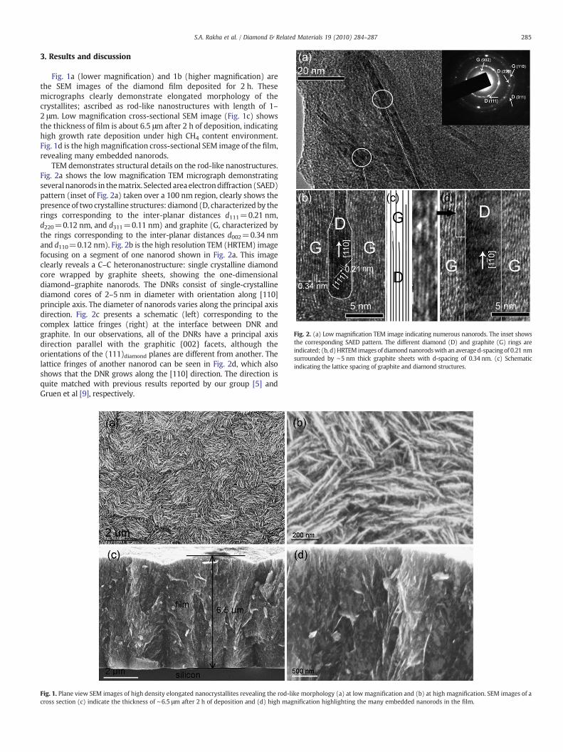
Fig. 2. (a) Low magnification TEM image indicating numerous nanorods. The inset showsthe corresponding SAED pattern. The different diamond (D) and graphite (G) rings areindicated; (b, d)HRTEM images of diamondnanorodswith an averaged-spacing of 0.21 nmsurrounded by ∼5 nm thick graphite sheets with d-spacing of 0.34 nm. (c) Schematicindicating the lattice spacing of graphite and diamond structures.
285S.A. Rakha et al. / Diamond & Related Materials 19 (2010) 284–287
3. Results and discussion
Fig. 1a (lower magnification) and 1b (higher magnification) arethe SEM images of the diamond film deposited for 2 h. Thesemicrographs clearly demonstrate elongated morphology of thecrystallites; ascribed as rod-like nanostructures with length of 1–2 μm. Low magnification cross-sectional SEM image (Fig. 1c) showsthe thickness of film is about 6.5 μm after 2 h of deposition, indicatinghigh growth rate deposition under high CH4 content environment.Fig. 1d is the highmagnification cross-sectional SEM image of the film,revealing many embedded nanorods.
TEM demonstrates structural details on the rod-like nanostructures.Fig. 2a shows the low magnification TEM micrograph demonstratingseveral nanorods in thematrix. Selected areaelectrondiffraction (SAED)pattern (inset of Fig. 2a) taken over a 100 nm region, clearly shows thepresence of two crystalline structures: diamond (D, characterized by therings corresponding to the inter-planar distances d111=0.21 nm,d220=0.12 nm, and d311=0.11 nm) and graphite (G, characterized bythe rings corresponding to the inter-planar distances d002=0.34 nmand d110=0.12 nm). Fig. 2b is the high resolution TEM (HRTEM) imagefocusing on a segment of one nanorod shown in Fig. 2a. This imageclearly reveals a C–C heteronanostructure: single crystalline diamondcore wrapped by graphite sheets, showing the one-dimensionaldiamond–graphite nanorods. The DNRs consist of single-crystallinediamond cores of 2–5 nm in diameter with orientation along [110]principle axis. The diameter of nanorods varies along the principal axisdirection. Fig. 2c presents a schematic (left) corresponding to thecomplex lattice fringes (right) at the interface between DNR andgraphite. In our observations, all of the DNRs have a principal axisdirection parallel with the graphitic {002} facets, although theorientations of the (111)diamond planes are different from another. Thelattice fringes of another nanorod can be seen in Fig. 2d, which alsoshows that the DNR grows along the [110] direction. The direction isquite matched with previous results reported by our group [5] andGruen et al [9], respectively.
Fig. 1. Plane view SEM images of high density elongated nanocrystallites revealing the rod-like morphology (a) at low magnification and (b) at high magnification. SEM images of across section (c) indicate the thickness of ∼6.5 μm after 2 h of deposition and (d) high magnification highlighting the many embedded nanorods in the film.

286 S.A. Rakha et al. / Diamond & Related Materials 19 (2010) 284–287
The XRD spectrum of the DNRs is shown in Fig. 3a. The spectrumindicates the diamond (111) and (220) diffraction peaks at 35.1° and59.1° respectively. The peak positions using X-rays of wavelength1.24 Å are shifted at 35.1° and 59.1° in comparison to X-ray diffractionspectrum using Cu Kα with wavelength 1.54 Å where these peaksappear at 43.9° and 75.1° respectively. The diffraction peak forgraphite (002) is at 20.8° 2theta value. The strong peak at 54.1° is Si(400) substrate peak. These results indicate the coexistence ofdiamond and graphite structure in the DNRs. The Raman spectrumcan exhibit main features associated with sp3 and sp2 carbon phases.For the high purity ultrafine diamond, it is well known that there is awide peak centered at approximately 1332 cm−1, if the 514.5 nmwavelength was adopted [10]. However, current Raman spectrum(Fig. 3b) shows that this diamond feature peak is completely coveredby the D band of graphite or amorphous carbon [11]. This indicates thehigh content of graphite and amorphous carbon in current film.Although, the weak band centered at approximately 1150 cm−1
indicates the existence of ultrafine nanodiamond [12–15]. Themicrostructural variations are the dominant factor affecting the sp2
bond contributions to the Raman spectra over the size range that wemeasured. The band at 1579 cm−1 is associated with G band ofgraphite [11]. The peak around 1610 cm−1 results from the vibrationarising due to the presence of sp2-bonded carbon clusters in thesample. Thus sp2 related defects other than graphite are also apparentfrom Raman spectrum of DNRs.
Since the discovery of zero-dimensional diamond heteronanos-tructure in the last decade [16], the synthesis of one-dimensional
Fig. 3. (a) XRD and (b) Raman spectrum of DNRs (SEM images shown in Fig. 1)indicating the characteristics peaks of diamond and graphite structure.
diamond heteronanostructures have received considerable attention[17–19]. It has been predicted [20] that the dehydrogenated {111}surfaces of diamond nanowires is unstable, andmuch probably will becovered by graphitic shells, leading to formation of the diamond–graphite heterostructures. The production of the present nanorodshas confirmed this prediction to a better extent.
As a metastable 1D nanostructure, DNRs can only grow in a criticalcondition, which should simultaneously meet both the metastablethermodynamic and 1D growth. The main factors leading to favorableconditions for synthesis of one-dimensional nanodiamond (Fig. 1) inMPCVD system are the high concentration of methane in Ar richenvironment decomposed using high microwave power. We foundthat under these conditions, the composite material has high sp3
carbon content in form of nanorods along with graphite sheetsurrounding the rods. It has been suggested in previous reports[9,18] that the addition of nitrogen played a critical role for one-dimensional nanodiamond growth in the Ar rich environment, by theformation of polymeric (CN) molecules as a template. Although highCH4 content increase the renucleation rate and suppress the size butthe polycyclic aromatic hydrocarbons (C–H) [21] and polymericchains like CN [22] in Ar/N2 plasma play the role in reducing therenucleation rate in the presence of H2 [22,23]. This creates favorableconditions for an increase of the grain size and the formation of one-dimensional diamond nanostructures.
However, in our experiments, the DNRs have also been grownwithout nitrogen addition (with Ar/H2/CH4 only, will be presentedelsewhere). The role for the formation of 1-Dimensional nanostruc-ture can be carried out by polyacetylene chains like C–H in the Ar richplasma in the absence of nitrogen. The excitation processes due tocollisionswith Ar+ and Ar* lead to the formation of a complexmixtureof organic molecules including trans-polyacetylene and polycyclicaromatic hydrocarbons [21], which helped to form suchnanostructures.
The results obtained after decreasing N2 content in the feed gases,from 40% upto 15% to 5% (Fig. 4a–b) demonstrates DNRs with lengthof 1–2 μm, suggested that N2 is not accounting the critical role for theproduction of DNRs. No considerable variations are observed in themorphology of nanocrystallites by decreasing nitrogen up to 5%.Fig. 4c shows the Raman spectra of the corresponding diamond films(SEM images shown in Fig. 4a–b). The presence of diamond phase(peak around 1332 cm−1) and of sp2 bonded carbon phase (“G” bandaround 1590 cm−1) are evident. A shoulder around 1150 cm−1 is dueto the transpolyacetylene (TPA) segments at the grain boundaries ofUNCD surface as discussed above. We observed that diamond peak isat 1332 cm−1 for the samples with 5%, and 15% of N2 (Fig. 4c), but it isoverlapped with D band for the sample with 40% N2 (Fig. 3b). Thisresult indicates the increase of the quantity of the sp2-bonded carbonwith the amount of nitrogen added to the synthesis gas. As thenitrogen addition increases, the long range ordering in the sp2 sitesincreases and the D peak becomes more prominent [24] indicatingthat nitrogen is more influential in term of structural changes ratherthan in morphology changes. According to our observations, theaddition of N2 is much helpful to increase the deposition rate and thecontent of one-dimensional structures, particularly for sp2-bondedgraphite/nondiamond content. On the other hand, it has beenconfirmed that at the boundaries of DNRs [9], the dominant objectis amorphous sp2-bonded carbon shells. Experimentally, very thingraphitic shells wrapping one side of diamond nanorod wereobserved by Vlasov et al [18] using the N2 added Ar rich MPCVD.We suggest that the dependence of nitrogen addition on morphologyis not a result of nitrogen incorporation but instead might be causedby nitrogen related surface processes by the changes in gas phasechemistry and surface kinetics [25]. These indicate that N2 played animportant role for the production of sp2-bonded carbon, andconsequently of graphitic shell surrounding the DNRs. The role ofhigh methane concentration in the production of graphite content

Fig. 4. SEM images of NCD films deposited with decreasing N2 upto; (a) 5%, and (b) 15%,(c) Raman spectra of the corresponding films.
287S.A. Rakha et al. / Diamond & Related Materials 19 (2010) 284–287
cannot be ignored as is reported by researchers [26]. The highmethane content is important due to two reasons: the methane issupplying the carbon source for the growth of DNRs and the highcarbon content is also helpful to facilitate the formation of C–H likepolyacetylene chains. If low methane content is used, no 1-D graphitediamond nanostructures were observed giving rise to the fact that
there must present enough carbon content to facilitate sp2 in sp3
dominated atmosphere. However, for the formation of DNRs the rolesof C2 carbon dimer [27], the principal growth species in Ar richenvironment, still needs to be considered and is open for furtherstudy.
4. Conclusions
In conclusion, diamond–graphite nanorods were synthesized by theMPCVD technique. The high methane content is necessary for theformation of polyacetylene chains which facilitate the one dimensionalgrowth of nanodiamond. The N2 addition in the Ar rich feeding gas isconsidered to play an important role for enhancing the content ofgraphite which served as the shells of the DNRs. Raman and X-raydiffraction spectra also indicated the existence of diamond and graphitephases in the film. This work proved the theoretical prediction on the{111} surfaces of diamond nanowires after dehydrogenation.
Acknowledgements
Financial support by Chinese Academy of Sciences KnowledgeInnovation Program (Grant No. KJCX3.SYW.N10) and National NaturalScience Foundation of China (No. 10775171) is gratefully acknowl-edged. The first author acknowledges the financial support by theGovernment of Pakistan.
References
[1] A. Geim, K. Novoselov, Science 306 (2004) 666.[2] H. Masuda, T. Yanagishita, K. Yasui, K. Nishio, I. Yagi, T.N. Rao, A. Fujishima, Adv.
Mater. 13 (2001) 247.[3] N.O. Alexander, P.G. Kopylov, A.L. Chuvilin, N.V. Savenko, Diamond Relat. Mater. 18
(2009) 1289.[4] W. Smirnov, A. Kriele, N. Yang, C. E. Nebel, Diamond Relat. Mater, doi:10.1016/j.
diamond.2009.09.001.[5] A.S. Barnard, S.P. Russo, I.K. Snook, Nano Lett. 3 (2003) 1323.[6] A.S. Barnard, I.K. Snook, J. Chem. Phys. 120 (2004) 3817.[7] L.T. Sun, J.L. Gong, Z.Y. Zhu, D.Z. Zhu, S.X. He, Adv. Mater. 16 (2004) 1849.[8] A.R. Sobia, G.J. Yu, X.T. Zhou, J. Crys. Growth. 13 (2009) 3332.[9] R. Arenal, P. Bruno, D.J. Miller, M. Bleuel, J. Lai, D.M. Gruen, Phys. Rev. B 75 (2007)
195431.[10] Y.M. LeGrice, R.J. Nemanich, J.T. Glass, Y.H. Lee, R.A. Rudder, R.J. Markunas, Mater.
Res. Symp. Proc. 62 (1990) 219.[11] S. Talapatra, J.Y. Cheng, N. Chakrapani, S. Trasobares, P.M. Ajayan, Nanotechnology
17 (2006) 305.[12] R.E. Shroder, R.J. Nemanich, J.T. Glass, Phys. Rev. B 41 (1990) 3738.[13] R.J. Nemanich, J.T. Glass, G. Lucovsky, J. Vat. Sci. Technol. A 6 (1988) 1783.[14] R. Pfeiffer, H. Kuzmany, P. Knoll, S. Bokova, N. Salk, B. Günther, Diamond Relat.
Mater. 12 (2003) 268.[15] H. Kuzmany, R. Pfeiffer, N. Salk, B. Günther Carbon 42 (2004) 911.[16] F. Banhart, P.M. Ajayan, Nature 382 (1996) 433.[17] X. Xiao, J.W. Elam, S. Trasobares, O. Auciello, J.A. Carlisle, Adv. Mater. 17 (2005)
1496.[18] I.I. Vlasov, O.I. Lebedev, V.G. Ralchenko, Adv. Mater. 19 (2007) 4058.[19] O.A. Shenderova, D. Areshkin, D.W. Brenner, Mol. Simulat. 29 (2003) 259.[20] A.S. Barnard, Rev. Adv. Mater. Sci. 6 (2004) 94.[21] N. Aggadi, C. Arnas, F. Benedic, C. Dominique, D.M. Gruen, Diamond Relat. Mater.
15 (2006) 908.[22] J. Birrell, J.A. Carlisle, O. Auciello, J.M. Gibson, Appl. Phys. Lett. 81 (2002) 2235.[23] P. Zapol, M. Sternberg, L.A. Curtiss, T. Frauenheim, D.M. Gruen, Phys. Rev. B 65
(2002) 045403.[24] R. Arenal, G. Montagnac, P. Bruno, D.M. Gruen, Phys, Rev. B 76 (2007) 245316.[25] G.Z. Cao, J.J. Schermer, W.J.P. van Enckevort, W.A.L.M. Elst, L.J. Giling, J. Appl. Phys.
79 (1996) 1357.[26] A. Afzal, C.A. Rego, W. Ahmed, R.I. Cherry, Diamond Relat. Mater. 7 (1998) 1033.[27] D. Zhou, T.G. McCauley, L.C. Qin, A.R. Krauss, D.M. Gruen, J. Appl. Phys. 83 (1998)
540.